EP0580085A2 - Circuit de surveillance de remplissage - Google Patents
Circuit de surveillance de remplissage Download PDFInfo
- Publication number
- EP0580085A2 EP0580085A2 EP93111417A EP93111417A EP0580085A2 EP 0580085 A2 EP0580085 A2 EP 0580085A2 EP 93111417 A EP93111417 A EP 93111417A EP 93111417 A EP93111417 A EP 93111417A EP 0580085 A2 EP0580085 A2 EP 0580085A2
- Authority
- EP
- European Patent Office
- Prior art keywords
- memory
- monitoring circuit
- level monitoring
- signal
- counting
- Prior art date
- Legal status (The legal status is an assumption and is not a legal conclusion. Google has not performed a legal analysis and makes no representation as to the accuracy of the status listed.)
- Granted
Links
Images

Classifications
-
- G—PHYSICS
- G11—INFORMATION STORAGE
- G11C—STATIC STORES
- G11C7/00—Arrangements for writing information into, or reading information out from, a digital store
Definitions
- the invention relates to a fill level monitoring circuit for an electronic memory module, the memory of which is supplied with a data stream, and which has a memory logic which combines the bits of the data stream stored in the memory into cells of a defined bit length, which can be tapped at a read output of the electronic memory module.
- Such an electronic memory module is known. It is used in ATM (Asynchronous Transfer Mode) communication systems.
- a disadvantage of the known electronic memory modules is that no exact monitoring of the fill level is provided. Memory modules are known which indicate that they are half or completely filled. This is done by using a "half-full bit", which indicates the corresponding memory allocation.
- a disadvantage of this type of monitoring is that there is a great delay in the data stream, since the memory of the electronic memory module only has to run half full before an indication occurs for the first time. Such a delay is particularly in the case of communication networks Very disadvantageous, since the maximum permissible delay time of the data from the sender to the receiver must not be exceeded. However, the individual delay times add up due to the data buffers required for the transmission, so that the above-mentioned monitoring of the fill level leads to intolerable delay times, in particular when generating ATM cells and when multiplexing the data streams.
- the object of the invention is to provide a fill level monitoring circuit for an electronic memory module of the type mentioned at the outset, which can detect the exact and rapid Allocation of memory enabled.
- the memory logic of the electronic memory module generates a count pulse memory signal for each complete cell of defined bit length, which is fed to a counting device of the fill level monitoring circuit, the count of which is incremented by the count pulse memory signal generated by the memory logic that the fill level monitoring circuit has an evaluation unit which periodically polls the counter reading of the counting device, and that the memory logic of the electronic memory module generates a confirmation memory signal after completion of a reading process of a cell, which is fed to the counting device of the fill level monitoring circuit, the counter reading of which is generated by the acknowledgment pulse generated by the storage logic Memory signal is decremented.
- the fill level monitoring circuit according to the invention is now particularly distinguished by the fact that it responds particularly quickly and works efficiently after just a few stored cells. It is therefore not necessary, as has been the case up to now, to wait for a memory to be half full in order to begin with a level-adaptive readout sequence. This has the advantage that there is only a minimal delay in the data streams.
- An advantageous development of the invention provides that the evaluation unit generates a readout signal as a function of the determined meter reading, which is fed to the memory logic of the electronic memory module, which then initiates the readout process of a cell.
- the fill level monitoring circuit according to the invention enables a fill level adaptive readout sequence of a plurality of electronic memory modules arranged in parallel, which have a different fill level due to the different data volumes supplied to them.
- the measures according to the invention also advantageously have the effect that the memories of the electronic memory modules can be optimally dimensioned, as a result of which the manufacturing costs of the memory modules are significantly reduced.
- An advantageous further development of the invention provides that in the signal path of the counting memory signal and the acknowledgment memory signal, a memory signal separating device is connected upstream of the counting device, which performs a temporal resolution of a counting pulse memory signal overlapping with the acknowledgment signal. This measure advantageously ensures that proper functioning of the counting device and thus of the fill level device is also ensured if a counting pulse memory signal incrementing the counter reading of the counting device and an acknowledgment memory signal decrementing this occur simultaneously.
- the exemplary embodiment shown in FIG. 1 has seven identically constructed electronic memory modules 10a-10g, the data input 10a'-10g 'of which a continuous data stream D1-D7 is supplied.
- the individual bits of each data stream D1-D7 are stored byte by byte in a manner known per se in a memory 11a-11g of the electronic memory module 10a-10g which is designed as a FIFO or as a dual-port RAM.
- This storage and the reading out of the stored data is controlled by a memory logic 12a-12g present in each electronic memory module 10a-10g.
- These memory logics 12a-12g also generate memory signals, the function of which will be explained in more detail below.
- the circuit shown in FIG. 1 also has an electronic memory module 10h with an empty cell memory 11h and with an associated memory logic 12h, in which so-called empty cells are stored. These should always be read out when the memories 11a-11g of the electronic memory modules 10a-10g are empty or their occupancy does not exceed a defined value.
- the data streams D1-D7 supplied to the individual memory chips 10a-10g generally have a different bit rate, so that the memories 11a-11g of the electronic memory chips 10a-10g are not filled uniformly.
- the different fill level of the individual memories 11a-11g of the electronic memory modules 10a-10g which is caused by the different data volume of the individual data streams D1-D7, now requires a level-adaptive readout sequence, so that an overflow of the memories 11a-11g is prevented.
- the memory 11a of the electronic memory component 10a has the highest fill level at the time in question.
- the fill level monitoring circuit 20 is used for this purpose, which periodically monitors the occupancy of the individual memories 11a-11g: the memory logic 12a-12g of each electronic memory module 10a-10g generates a counting pulse memory signal CC1-CC7 for this purpose, which is fed to the fill level monitoring circuit 20.
- This count pulse memory signal CC1-CC7 is generated whenever a defined number of bytes has been written into one of the memories 11a-11g, so that the memory logic 12a-12g of the relevant electronic memory chip 10a-10g it can form a cell with a defined bit length.
- the count pulse memory signal CC1-CC7 is always generated when the abovementioned number of bytes in a memory of the memories 11a -11g of the electronic memory modules 10a-10g has been stored.
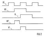
- the memory logic 12a of the electronic memory module 10a generates the counting pulse memory signal CC1, which is preferably represented by a rectangular pulse which has the duration of a system clock ST which controls the signal processing of the exemplary embodiment (cf. FIG. 2).
- the individual count pulse memory signals CC1-CC7 are each routed via a memory signal separating device 50a-50g, which is described in more detail below, to an associated counting device 30a-30g of the fill-level monitoring circuit 20 and increment their counter reading.
- the fill level monitoring circuit 20 also has a further counting device 30h, which is functionally assigned to the empty cell memory 11h. This further counter 30h - whose function is described below - has a fixed counter reading, which can be preset as desired.
- An evaluation device 40 of the fill level monitoring circuit 20 periodically calls up the current counter readings of the counter devices 30a-30g and the further counter device 30h with a divided system clock ST and compares the counter readings of the individual counter devices of the electronic memory modules 10a-10h with one another.
- the evaluation device 40 in a first step in pairs the higher counter reading of the first and the second 30a and 30b or the third and fourth 30c and 30d or the fifth and sixth 30e and 30f or the seventh and the further counter 30g and 30h determined.
- the higher value of the two first counter readings compared with each other, determined from this pair-wise comparison, is compared in a second step with the higher counter readings of the third and fourth counter devices 30c and 30d, etc., so that with eight counter devices after three such steps the electronic memory module (10a) is determined whose memory (11a) has the highest fill level.
- the evaluation device 40 of the The fill level monitoring device 20 then generates a coded readout signal containing the address of the memory 11a to be read, which is fed via a data bus 80 to the control logic 12a of the electronic memory module 10a.
- the memory logic 12a addressed by the readout signal then initiates the readout process of a cell from the memory 11a.
- the memory logic 12a After the last byte of the cell to be read, which is routed via a data line 60 to a switching center 60, not shown in FIG the memory logic 12a generates an acknowledgment memory signal Q1-Q7 (here: Q1), which is fed via the memory signal separating device 50a-50g to that counting unit (30a) of the evaluation device 40 which is assigned to the read-out memory (10a).
- the acknowledgment memory signal Q1-Q7 generated in each case by the memory logic 12a-12g has the effect that the counter reading of the corresponding counter device 30a-30g (here: 30a) of the fill-level monitoring circuit 20 is decremented.
- the advantage here is that the counter reading of the further counter 30h is preset to a defined value is.
- the specification of a fixed counter reading of the further counter device 30h means that the reading process of the cells from the memories 11a-11g only begins when their fill level has reached the preset value of the meter reading of the other meter. In this way, it is easily possible to prioritize the sequential readout of the data stream with the highest bit rate for level adaptation.
- each counting device 30a-30h Alternatively or in addition to this, it is possible to give each counting device 30a-30h a different starting value of the counter reading for the purpose of prioritization.
- memory signal separation devices 50a-50g which each exist between an electronic memory module 10a-10g and the associated counting device 30a-30g of the fill level monitoring circuit 20 are connected in the signal path of the counting pulse and acknowledgment memory signals CC1-CC7 and Q1-Q7.
- These memory signal separators 50a-50g serve to temporally dissolve the memory signals CC1-CC7 or Q1-Q7 generated by the memory logic 12a-12g of each memory module - which correspond to different counting directions of the counting unit - so that the counting devices 30a function properly. 30g of the fill level monitoring device 20 is guaranteed.
- the function of one of the memory signal separators 50a-50g is explained with reference to FIG. 2.
- the course of the system clock ST controlling the signal processing of the exemplary embodiment is shown in the first line.
- the second line of FIG. 2 shows the count pulse memory signal generated by one of the memory logics 12a-12g, the electronic memory chips 10a-10g, which is generally designated CC.
- the time course of the counting pulse memory signal CC is such that it only assumes the logical value "1" for the duration of a period of the system clock ST if so many bits of the data stream D1-D7 supplied to the respective memory 11a-11g have already been stored so that the memory logic 12a-12g of the each electronic memory chip 10a-10g can form a new cell of defined bit length therefrom.
- the memories 11a-11g of the electronic memory modules 10a-10g enable both a write and a readout of a cell simultaneously, it is conceivable that - as shown in line 3 of FIG -12g both a counting pulse CC and an acknowledgment signal Q is generated. If the assigned counting device 30a-30g is controlled with such a signal constellation, i.e. If a counting pulse memory signal CC incrementing the counting device 30a-30g and a confirmation memory signal Q decrementing it occur simultaneously in the same system clock ST, a counting error of the counting device 30a-30g cannot be ruled out in the case of such overlapping memory signals.
- the two memory signals CC and Q are separated in time in the memory signal separating device 50a-50g, so that this overlapping state is eliminated.
- the logical "1" state of the counting memory signal CC representing a counting pulse is shortened in such a way that it is somewhat corresponds to less than half a period of the system clock ST (CC ').
- the "1" state of the acknowledgment memory signal Q is shortened (Q1). This measure makes it particularly easy to achieve perfect functioning of the counting devices 30a-30g even with memory signals that overlap in time.
Landscapes
- Data Exchanges In Wide-Area Networks (AREA)
- Techniques For Improving Reliability Of Storages (AREA)
- Debugging And Monitoring (AREA)
- Static Random-Access Memory (AREA)
- Semiconductor Memories (AREA)
- Input Circuits Of Receivers And Coupling Of Receivers And Audio Equipment (AREA)
- Monitoring And Testing Of Exchanges (AREA)
- Measurement Of Current Or Voltage (AREA)
Applications Claiming Priority (2)
| Application Number | Priority Date | Filing Date | Title |
|---|---|---|---|
| DE4224421 | 1992-07-24 | ||
| DE4224421A DE4224421A1 (de) | 1992-07-24 | 1992-07-24 | Füllstandsüberwachungsschaltung |
Publications (3)
| Publication Number | Publication Date |
|---|---|
| EP0580085A2 true EP0580085A2 (fr) | 1994-01-26 |
| EP0580085A3 EP0580085A3 (en) | 1995-12-20 |
| EP0580085B1 EP0580085B1 (fr) | 1998-03-18 |
Family
ID=6463972
Family Applications (1)
| Application Number | Title | Priority Date | Filing Date |
|---|---|---|---|
| EP93111417A Expired - Lifetime EP0580085B1 (fr) | 1992-07-24 | 1993-07-16 | Composant de dispositif de mémoire |
Country Status (5)
| Country | Link |
|---|---|
| EP (1) | EP0580085B1 (fr) |
| AT (1) | ATE164256T1 (fr) |
| AU (1) | AU665428B2 (fr) |
| DE (2) | DE4224421A1 (fr) |
| ES (1) | ES2114976T3 (fr) |
Cited By (2)
| Publication number | Priority date | Publication date | Assignee | Title |
|---|---|---|---|---|
| WO1997008703A1 (fr) * | 1995-08-30 | 1997-03-06 | Micron Technology, Inc. | Memoire a acces sequentiel sam a largeur de donnees extensible pour une memoire vive a acces multiples |
| US6487207B1 (en) | 1997-02-26 | 2002-11-26 | Micron Technology, Inc. | Shared buffer memory architecture for asynchronous transfer mode switching and multiplexing technology |
Family Cites Families (4)
| Publication number | Priority date | Publication date | Assignee | Title |
|---|---|---|---|---|
| US4592019A (en) * | 1983-08-31 | 1986-05-27 | At&T Bell Laboratories | Bus oriented LIFO/FIFO memory |
| DE3732937A1 (de) * | 1987-09-30 | 1989-04-20 | Philips Patentverwaltung | Schaltungsanordnung zur vermeidung von ueberlast in einem breitband-vermittlungssystem |
| ATE149069T1 (de) * | 1989-09-29 | 1997-03-15 | Siemens Ag | Schaltungsanordnung zum ermitteln der einer atm- vermittlungsanlage im zuge von virtuellen verbindungen jeweils zugeführten nachrichtensignalmenge und zur überprüfung der einhaltung festgelegter bitraten |
| DE4012768A1 (de) * | 1990-04-21 | 1991-10-24 | Philips Patentverwaltung | Koppelelement |
-
1992
- 1992-07-24 DE DE4224421A patent/DE4224421A1/de not_active Withdrawn
-
1993
- 1993-07-13 AU AU41876/93A patent/AU665428B2/en not_active Ceased
- 1993-07-16 AT AT93111417T patent/ATE164256T1/de not_active IP Right Cessation
- 1993-07-16 ES ES93111417T patent/ES2114976T3/es not_active Expired - Lifetime
- 1993-07-16 DE DE59308271T patent/DE59308271D1/de not_active Expired - Fee Related
- 1993-07-16 EP EP93111417A patent/EP0580085B1/fr not_active Expired - Lifetime
Cited By (4)
| Publication number | Priority date | Publication date | Assignee | Title |
|---|---|---|---|---|
| WO1997008703A1 (fr) * | 1995-08-30 | 1997-03-06 | Micron Technology, Inc. | Memoire a acces sequentiel sam a largeur de donnees extensible pour une memoire vive a acces multiples |
| US5657289A (en) * | 1995-08-30 | 1997-08-12 | Micron Technology, Inc. | Expandable data width SAM for a multiport RAM |
| US5717647A (en) * | 1995-08-30 | 1998-02-10 | Micron Technology, Inc. | Expandable data width sam for a multiport ram |
| US6487207B1 (en) | 1997-02-26 | 2002-11-26 | Micron Technology, Inc. | Shared buffer memory architecture for asynchronous transfer mode switching and multiplexing technology |
Also Published As
| Publication number | Publication date |
|---|---|
| AU665428B2 (en) | 1996-01-04 |
| AU4187693A (en) | 1994-01-27 |
| DE4224421A1 (de) | 1994-01-27 |
| ES2114976T3 (es) | 1998-06-16 |
| ATE164256T1 (de) | 1998-04-15 |
| EP0580085B1 (fr) | 1998-03-18 |
| EP0580085A3 (en) | 1995-12-20 |
| DE59308271D1 (de) | 1998-04-23 |
Similar Documents
| Publication | Publication Date | Title |
|---|---|---|
| DE4019135C2 (de) | Serieller Speicher auf RAM-Basis mit parallelem Voraus-Lesen und Verfahren zum Speichern von Datenelementen in eine serielle Speichervorrichtung | |
| DE2637004C2 (de) | Dynamischer Halbleiterspeicher | |
| EP0529358B1 (fr) | Unité de mémoire avec générateur d'adresses | |
| EP0419958B1 (fr) | Circuit dans un central de commutation à multiplexage temporel asynchrone pour détecter la quantité de données transmises et pour contrÔler la conformité avec des taux de bits specifiés | |
| EP1101329B1 (fr) | Module de pontage | |
| DE3107232A1 (de) | Elastischer speicher hoher kapazitaet und mit kontinuierlich veraenderbarer verzoegerung | |
| EP0419959B1 (fr) | Circuit pour contrÔler le respet de débits préétablis lors de la transmission de cellules de données | |
| EP0475498B1 (fr) | Circuit d'adaption du débit binaire de deux signaux numériques | |
| EP0031485A1 (fr) | Dispositif de priorité pour unité de système de traitement de données avec une barre omnibus | |
| DE102015120242B3 (de) | Verfahren zum Betreiben eines Kommunikationsnetzwerkes, Kommunikationsnetzwerk, Steuervorrichtung und Datenverarbeitungsvorrichtung | |
| WO2001020416A2 (fr) | Transmission de donnees serielle par l'intermediaire d'un systeme a bus | |
| EP0580085B1 (fr) | Composant de dispositif de mémoire | |
| WO2000007093A1 (fr) | Dispositif a memoire et son procede de fonctionnement | |
| DE19627728A1 (de) | Netzelement und Ein-/Ausgabeeinheit für ein synchrones Übertragungssystem | |
| DE2908366C2 (de) | Verfahren und Schaltungsanordnung zur Reduzierung von Phasenschwankungen bei der Taktrückgewinnung in einem digitalen, hierarchisch gegliederten, plesiochronen Nachrichtenübertragungssystem | |
| DE69232010T2 (de) | Vermittlungseinheit zwischen Eingängen und Ausgängen eines Kommunikationssystems | |
| DE4417286A1 (de) | Verfahren und Schaltungsanordnung zum Auslesen von Daten aus Pufferspeichern in ATM-Einrichtungen | |
| DE2702055A1 (de) | Datenuebertragungssystem | |
| DE2652038C2 (de) | System zur zentralen Erzeugung eines envelopeverschachtelten Zeitmultiplexsignals | |
| EP0180793B1 (fr) | Disposition pour la conversion de mots codés à longueur variable en mots de données à longueur constante | |
| DE2150930C3 (de) | Alarmeingabeschaltung für eine Datenverarbeitungsanlage | |
| EP0191421B1 (fr) | Circuit de surveillance pour signaux numériques | |
| DE2620493A1 (de) | Verfahren und vorrichtung zur uebertragung von daten zwischen einer steuereinheit und einem oder mehreren teilnehmern | |
| EP0263960B1 (fr) | Circuit de transmission de signaux de données | |
| DE3443616C2 (fr) |
Legal Events
| Date | Code | Title | Description |
|---|---|---|---|
| PUAI | Public reference made under article 153(3) epc to a published international application that has entered the european phase |
Free format text: ORIGINAL CODE: 0009012 |
|
| AK | Designated contracting states |
Kind code of ref document: A2 Designated state(s): AT BE CH DE ES FR GB IT LI NL SE |
|
| PUAL | Search report despatched |
Free format text: ORIGINAL CODE: 0009013 |
|
| AK | Designated contracting states |
Kind code of ref document: A3 Designated state(s): AT BE CH DE ES FR GB IT LI NL SE |
|
| 17P | Request for examination filed |
Effective date: 19960215 |
|
| 17Q | First examination report despatched |
Effective date: 19961106 |
|
| GRAG | Despatch of communication of intention to grant |
Free format text: ORIGINAL CODE: EPIDOS AGRA |
|
| GRAG | Despatch of communication of intention to grant |
Free format text: ORIGINAL CODE: EPIDOS AGRA |
|
| GRAG | Despatch of communication of intention to grant |
Free format text: ORIGINAL CODE: EPIDOS AGRA |
|
| GRAH | Despatch of communication of intention to grant a patent |
Free format text: ORIGINAL CODE: EPIDOS IGRA |
|
| GRAH | Despatch of communication of intention to grant a patent |
Free format text: ORIGINAL CODE: EPIDOS IGRA |
|
| RAP1 | Party data changed (applicant data changed or rights of an application transferred) |
Owner name: ALCATEL ALSTHOM COMPAGNIE GENERALE D'ELECTRICITE |
|
| GRAA | (expected) grant |
Free format text: ORIGINAL CODE: 0009210 |
|
| AK | Designated contracting states |
Kind code of ref document: B1 Designated state(s): AT BE CH DE ES FR GB IT LI NL SE |
|
| PG25 | Lapsed in a contracting state [announced via postgrant information from national office to epo] |
Ref country code: NL Free format text: LAPSE BECAUSE OF FAILURE TO SUBMIT A TRANSLATION OF THE DESCRIPTION OR TO PAY THE FEE WITHIN THE PRESCRIBED TIME-LIMIT Effective date: 19980318 |
|
| REF | Corresponds to: |
Ref document number: 164256 Country of ref document: AT Date of ref document: 19980415 Kind code of ref document: T |
|
| ITF | It: translation for a ep patent filed | ||
| REG | Reference to a national code |
Ref country code: CH Ref legal event code: EP |
|
| REF | Corresponds to: |
Ref document number: 59308271 Country of ref document: DE Date of ref document: 19980423 |
|
| GBT | Gb: translation of ep patent filed (gb section 77(6)(a)/1977) |
Effective date: 19980518 |
|
| PGFP | Annual fee paid to national office [announced via postgrant information from national office to epo] |
Ref country code: GB Payment date: 19980612 Year of fee payment: 6 |
|
| REG | Reference to a national code |
Ref country code: ES Ref legal event code: FG2A Ref document number: 2114976 Country of ref document: ES Kind code of ref document: T3 |
|
| PGFP | Annual fee paid to national office [announced via postgrant information from national office to epo] |
Ref country code: SE Payment date: 19980624 Year of fee payment: 6 |
|
| PGFP | Annual fee paid to national office [announced via postgrant information from national office to epo] |
Ref country code: AT Payment date: 19980625 Year of fee payment: 6 |
|
| PGFP | Annual fee paid to national office [announced via postgrant information from national office to epo] |
Ref country code: FR Payment date: 19980629 Year of fee payment: 6 |
|
| PGFP | Annual fee paid to national office [announced via postgrant information from national office to epo] |
Ref country code: DE Payment date: 19980630 Year of fee payment: 6 |
|
| PGFP | Annual fee paid to national office [announced via postgrant information from national office to epo] |
Ref country code: BE Payment date: 19980709 Year of fee payment: 6 |
|
| ET | Fr: translation filed | ||
| PGFP | Annual fee paid to national office [announced via postgrant information from national office to epo] |
Ref country code: ES Payment date: 19980716 Year of fee payment: 6 |
|
| PG25 | Lapsed in a contracting state [announced via postgrant information from national office to epo] |
Ref country code: LI Free format text: LAPSE BECAUSE OF NON-PAYMENT OF DUE FEES Effective date: 19980731 Ref country code: CH Free format text: LAPSE BECAUSE OF NON-PAYMENT OF DUE FEES Effective date: 19980731 |
|
| NLV1 | Nl: lapsed or annulled due to failure to fulfill the requirements of art. 29p and 29m of the patents act | ||
| PLBE | No opposition filed within time limit |
Free format text: ORIGINAL CODE: 0009261 |
|
| STAA | Information on the status of an ep patent application or granted ep patent |
Free format text: STATUS: NO OPPOSITION FILED WITHIN TIME LIMIT |
|
| RAP4 | Party data changed (patent owner data changed or rights of a patent transferred) |
Owner name: ALCATEL |
|
| 26N | No opposition filed | ||
| REG | Reference to a national code |
Ref country code: CH Ref legal event code: PL |
|
| PG25 | Lapsed in a contracting state [announced via postgrant information from national office to epo] |
Ref country code: GB Free format text: LAPSE BECAUSE OF NON-PAYMENT OF DUE FEES Effective date: 19990716 Ref country code: AT Free format text: LAPSE BECAUSE OF NON-PAYMENT OF DUE FEES Effective date: 19990716 |
|
| PG25 | Lapsed in a contracting state [announced via postgrant information from national office to epo] |
Ref country code: ES Free format text: LAPSE BECAUSE OF NON-PAYMENT OF DUE FEES Effective date: 19990717 |
|
| PG25 | Lapsed in a contracting state [announced via postgrant information from national office to epo] |
Ref country code: SE Free format text: THE PATENT HAS BEEN ANNULLED BY A DECISION OF A NATIONAL AUTHORITY Effective date: 19990730 |
|
| PG25 | Lapsed in a contracting state [announced via postgrant information from national office to epo] |
Ref country code: FR Free format text: THE PATENT HAS BEEN ANNULLED BY A DECISION OF A NATIONAL AUTHORITY Effective date: 19990731 Ref country code: BE Free format text: LAPSE BECAUSE OF NON-PAYMENT OF DUE FEES Effective date: 19990731 |
|
| REG | Reference to a national code |
Ref country code: FR Ref legal event code: CD |
|
| BERE | Be: lapsed |
Owner name: ALCATEL ALSTHOM CIE GENERALE D'ELECTRICITE Effective date: 19990731 |
|
| GBPC | Gb: european patent ceased through non-payment of renewal fee |
Effective date: 19990716 |
|
| EUG | Se: european patent has lapsed |
Ref document number: 93111417.7 |
|
| PG25 | Lapsed in a contracting state [announced via postgrant information from national office to epo] |
Ref country code: DE Free format text: LAPSE BECAUSE OF NON-PAYMENT OF DUE FEES Effective date: 20000503 |
|
| REG | Reference to a national code |
Ref country code: FR Ref legal event code: ST |
|
| REG | Reference to a national code |
Ref country code: ES Ref legal event code: FD2A Effective date: 20000810 |
|
| PG25 | Lapsed in a contracting state [announced via postgrant information from national office to epo] |
Ref country code: IT Free format text: LAPSE BECAUSE OF NON-PAYMENT OF DUE FEES;WARNING: LAPSES OF ITALIAN PATENTS WITH EFFECTIVE DATE BEFORE 2007 MAY HAVE OCCURRED AT ANY TIME BEFORE 2007. THE CORRECT EFFECTIVE DATE MAY BE DIFFERENT FROM THE ONE RECORDED. Effective date: 20050716 |