EP0580085B1 - Composant de dispositif de mémoire - Google Patents
Composant de dispositif de mémoire Download PDFInfo
- Publication number
- EP0580085B1 EP0580085B1 EP93111417A EP93111417A EP0580085B1 EP 0580085 B1 EP0580085 B1 EP 0580085B1 EP 93111417 A EP93111417 A EP 93111417A EP 93111417 A EP93111417 A EP 93111417A EP 0580085 B1 EP0580085 B1 EP 0580085B1
- Authority
- EP
- European Patent Office
- Prior art keywords
- memory
- memory module
- signal
- counting
- counter reading
- Prior art date
- Legal status (The legal status is an assumption and is not a legal conclusion. Google has not performed a legal analysis and makes no representation as to the accuracy of the status listed.)
- Expired - Lifetime
Links
Images

Classifications
-
- G—PHYSICS
- G11—INFORMATION STORAGE
- G11C—STATIC STORES
- G11C7/00—Arrangements for writing information into, or reading information out from, a digital store
Definitions
- the invention relates to a memory chip arrangement with an electronic memory module, its memory Data stream is supplied, and the storage logic which has the bits of the Data streams summarized into cells of defined bit length, the at a reading output of the electronic memory module Can be tapped, wherein the memory logic of the electronic memory module generates a counting pulse memory signal for each complete cell of defined bit length, which is fed to a counting device of a fill level monitoring circuit, the count of which is incremented by the counting pulse memory signal generated by the memory logic.
- Such an electronic memory module is known. He is used in ATM (Asynchronous Transfer Mode) communication systems used.
- a disadvantage of the known electronic Memory modules is that no exact monitoring of the Level is provided. They are memory modules known to indicate that they are half or completely filled. This is done by using a "half full bit", which shows the corresponding memory usage. Disadvantageous What is important about this type of monitoring is that it is a major one Delay in the data stream occurs because the memory of the electronic memory module only has to run half full, until an ad appears for the first time. Such Delay is especially with communication networks very disadvantageous, since the maximum permissible No delay time of the data from the sender to the receiver may be exceeded. Because of the transfer the required data buffers add up Delay times so that the above Monitoring the Level especially when generating ATM cells and when Multiplexing of data streams to no longer tolerable Delay times leads.
- the invention has the task of one electronic memory chip of the type mentioned and one Fill level monitoring circuit to create a memory chip arrangement which the level monitoring circuit an exact and rapid detection of Allocation of memory enabled.
- the Fill level monitoring circuit has an evaluation unit, which periodically queries the counter reading of the counter, and that the memory logic of the electronic memory chip after a cell has been read out Acknowledgment memory signal generated by the counter of the Level monitoring circuit is supplied, the Meter reading by the generated by the memory logic Acknowledgment pulse memory signal is decremented.
- the measures according to the invention in particular advantageous way easy and quick an exact Determination of the fill level of the memory of an electronic Memory module reached.
- Level monitoring circuit now stands out particularly in that it responds particularly quickly and efficient after just a few stored cells is working. One is therefore not - as before - forced to wait for a memory to be half full to get one level-adaptive readout sequence to begin. This has the Advantage that there is only a minimal delay in the data streams occurs.
- An advantageous development of the invention provides that the evaluation unit depending on the determined Counter reading generates a read signal that the memory logic of the electronic memory module is supplied, which then initiated the reading process of a cell. Due to the level monitoring circuit contained according to the invention a level-adaptive readout sequence of several in parallel arranged electronic memory chips, which conditionally due to the different data volumes supplied to them, have a different fill level, possible.
- the Measures according to the invention also have an advantageous effect Way that the memory of the electronic Memory chips can be optimally dimensioned, which means the manufacturing costs of the memory chips become clear to reduce.
- An advantageous development of the invention provides that in the signal path of the count memory signal and Acknowledgment memory signal each one of the counting device upstream memory signal separator is connected, which is a temporal resolution of one with the Acknowledgment signal overlapping count memory signal carries out. This measure is advantageous achieves that the counting device functions properly and thus the level device is also guaranteed is, if at the same time the counter reading of the counter incremental count memory signal and one decrementing acknowledgment memory signal occur.
- the embodiment shown in Figure 1 has seven identically structured electronic memory modules 10a-10g, whose data input 10a'-10g 'each one continuous data stream D1-D7 is supplied.
- the individual bits of each data stream D1-D7 are shown in known in a manner known as a FIFO or as Dual-port RAM running memory 11a-11g of electronic Memory blocks 10a-10g are stored in bytes. This Saving and reading out the stored data one in each electronic memory device 10a-10g existing memory logic 12a-12g controlled.
- This Memory logic 12a-12g also generate Memory signals, the function of which will be explained in more detail below will be explained.
- the circuit shown in Figure 1 also has an electronic memory chip 10h with a Empty cell memory 11h and with an associated one Memory logic 12h, in which so-called empty cells are stored will. These should always be read out when the Memory 11a-11g of the electronic memory modules 10a-10g are empty or their assignment does not have a defined value exceeds.
- the fed to the individual memory chips 10a-10g Data streams D1-D7 generally have a different one Bit rate so that the memory 11a-11g of the electronic Memory modules 10a-10g cannot be filled evenly. Due to the different data volume of the individual Data streams D1-D7 caused different fill levels of the individual memory 11a-11g of electronic Memory chips 10a-10g now require one Level adaptive readout sequence, so that an overflow of the Memory 11a-11g is prevented.
- Level adaptive readout sequence so that an overflow of the Memory 11a-11g is prevented.
- the fill level monitoring circuit 20 which the allocation of the individual memories 11a-11g periodically monitors: the storage logic 12a-12g of each Electronic memory module 10a-10g generates a for this Count memory signal CC1-CC7, which the Level monitoring circuit 20 is supplied.
- This Count memory signal CC1-CC7 is always generated if in one of the memories 11a-11g a defined number of Bytes was written so that the memory logic 12a-12g of the relevant electronic memory module 10a-10g it can form a cell with a defined bit length. For example, one of the CCITT recommendation I.361 corresponding ATM communication system, at the 48th Data bytes are combined into a cell, always then the count memory signal CC1-CC7 generates when the above.
- the Memory logic 12a of the electronic memory module 10a Count memory signal CC1, which is preferably by a rectangular pulse is represented, which is the duration of a control the signal processing of the embodiment System clock ST (cf. Fig. 2).
- the individual count memory signals CC1-CC7 are each via one described in more detail below Memory signal separator 50a-50g, one each assigned counter 30a-30g of the Level monitoring circuit 20 passed and increment their counter reading.
- the fill level monitoring circuit 20 also has another counting device 30h, which is functionally assigned to the empty cell memory 11h. This further counter 30h - its function continues is described below - has a fixed counter reading, which can be preset as desired.
- An evaluation device 40 of the Level monitoring circuit 20 calls periodically with a shared system clock ST the current counter readings of Counters 30a-30g and the other counter 30h and compares the meter readings of the individual Counting devices of the electronic memory modules 10a-10h among themselves.
- the evaluation device 40 in one first step in pairs the higher meter reading of the first and second 30a and 30b and third and the fourth 30c and 30d and fifth and sixth 30e and 30f or the seventh and further counting device 30g and 30h determined.
- the one from this pairwise comparison determined the higher value of the first two with each other
- the counter readings are compared in a second step again with the higher counter reading of the third and the fourth counter 30c and 30d compared, etc. compared so that with eight counters after three such steps the electronic memory chip (10a) is determined, the memory (11a) of which is the highest Level.
- the evaluation device 40 of the Level monitoring device 20 then generates a encodes the address of the memory to be read 11a containing readout signal, which via a data bus 80 Control logic 12a of the electronic memory module 10a is fed. The addressed by the readout signal Memory logic 12a then initiates the readout process Cell from memory 11a.
- the advantage here is that the counter reading of the other Counter 30h preset to a defined value is. As from the determination of the highest described above Meter reading of all counting devices 30a-30h easily can be seen, causes a fixed counter reading the further counter 30h that the reading process of the Cells from the memories 11a-11g only begin when their Level the preset value of the counter reading of the another counter. It is easily possible that way the data stream with the highest bit rate at level adapt, sequential readout prioritize.
- Memory signal separators 50a-50g each between an electronic memory chip 10a-10g and the associated counter 30a-30g Level monitoring circuit 20 in the signal path of the Count pulse and acknowledge memory signals CC1-CC7 and Q1-Q7 are switched. These memory signal separators 50a-50g are used by the storage logic 12a-12g each memory chip generates memory signals CC1-CC7 or Q1-Q7 - what different counting directions the Corresponding counting unit - to be resolved temporally so that a perfect functioning of the counters 30a-30g Level monitoring device 20 is guaranteed.
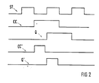
- the function of one of the memory signal separators 50a-50g is explained with reference to FIG. 2.
- On the first line is the course of the signal processing of the Embodiment controlling system clock ST shown.
- the second line of Figure 2 shows that from one of the Memory logic 12a-12g the electronic memory chips 10a-10g generated count memory signal, which is general is called CC.
- the time course of the Count pulse memory signal CC is such that this only then for the duration of a period of the system clock ST assumes logic value "1" if so many bits of the data stream D1-D7 supplied to respective memories 11a-11g were stored so that the memory logic 12a-12g of the respective electronic memory module 10a-10g therefrom can form a new cell of defined bit length.
- the two Memory signals CC and Q are separated in time, so that this state of overlap is eliminated.
- the one Count representing logical "1" state of the Count memory signal CC shortened so that it something corresponds to less than half a period of the system clock ST (CC ').
- the fifth line of the Figure 2 can be seen - the "1" state of the Acknowledgment memory signal Q shortened (Q1).
Landscapes
- Data Exchanges In Wide-Area Networks (AREA)
- Techniques For Improving Reliability Of Storages (AREA)
- Debugging And Monitoring (AREA)
- Static Random-Access Memory (AREA)
- Semiconductor Memories (AREA)
- Input Circuits Of Receivers And Coupling Of Receivers And Audio Equipment (AREA)
- Monitoring And Testing Of Exchanges (AREA)
- Measurement Of Current Or Voltage (AREA)
Claims (10)
- Configuration d'un composant de mémoire comprenant un composant de mémoire électronique (10a-10g ; 10h), un flux de données (D1-D7) étant acheminé vers la mémoire (11a-11g) dudit composant électronique, qui comporte une logique de mémoire (12a-12g), qui regroupe les bits du flux de données (D1-D7), stockés dans la mémoire (11a-11g), sous forme de cellules avec des longueurs de bits définies, qui peuvent être captées à la sortie de lecture (10a"-10g") du composant de mémoire électronique (10a-10g), la logique de mémoire (12a-12g) du composant de mémoire électronique (10a-10g) émettant pour chaque cellule complète d'une longueur de bits définie un signal mémoire d'une impulsion de comptage (CC1-CC7 ; CC), lequel signal est acheminé vers un compteur (30a-30g) d'un circuit de surveillance du niveau d'occupation de la mémoire (20), dont la position du compteur est incrémentée par le signal mémoire d'une impulsion de comptage (CC1-CC7 ; CC) émis par la logique de mémoire (12a-12g), caractérisée en ce que le circuit de surveillance du niveau d'occupation (20) comporte une unité d'analyse (40), qui interroge périodiquement la position du compteur (30a-30g) et en ce que la logique de mémoire (12a-12g) du composant de mémoire électronique émet un signal mémorie de confirmation (Q1-Q7 ; Q) à la fin du processus de lecture d'une cellule de mémoire, lequel signal est acheminé vers le compteur (30a-30g) du circuit de surveillance du niveau d'occupation (20), dont la position est décrémentée par le signal mémoire de l'impulsion de confirmation émis par la logique de mémoire.
- Configuration d'un composant de mémoire selon la revendication 1, caractérisée en ce que l'unité d'analyse (40) émet un signal de lecture en fonction de la position du compteur déterminée, lequel signal est acheminé vers la logique de mémoire (12a-12h) de l'un des composants de mémoire électroniques (10a-10h), qui initialise ensuite le processus de lecture d'une cellule de mémoire.
- Configuration d'un composant de mémoire selon la revendication 1, caractérisée en ce que, dans le trajet des signaux mémoire (CC1-CC7 ; Q1-Q7) et en amont du compteur (30a-30g) de l'unité d'analyse (40), est monté un dispositif de séparation du signal mémoire (50a-50g), qui exécute une décomposition en fonction du temps d'un signal mémoire d'une impulsion de comptage (CC1-CC7 ; CC) qui chevauche le signal mémoire de confirmation (Q1-Q7 ; Q).
- Configuration d'un composant de mémoire selon la revendication 3, caractérisée en ce que le dispositif de séparation du signal mémoire (50a-50g) réduit la durée d'impulsion du signal mémoire d'une impulsion de comptage (CC1-CC7 ; CC) et du signal mémoire de confirmation (Q1-Q7 ; Q) à un espace de temps qui est inférieur à une demi-période du cycle du système (ST) qui commande le traitement du signal.
- Configuration d'un composant de mémoire selon l'une quelconque des revendications 1 à 4, comprenant plusieurs composants de mémoire électroniques (10a-10g), montés en parallèle et dont chaque entrée de données (10a'-10g') capte un flux de données (D1-D7), caractérisée en ce que chaque logique de mémoire (12a-12g) de chaque composant de mémoire électronique (10a-10g) est reliée à un compteur (30a-30g) du circuit de surveillance du niveau d'occupation (20), en ce que l'unité d'analyse (40) interroge périodiquement la position de tous les compteurs (30a-30g) et détermine le compteur (30a) présentant la position la plus élevée.
- Configuration d'un composant de mémoire selon la revendication 5, caractérisée en ce que le dispositif d'analyse (40) émet un signal de lecture, qui contient l'adresse sous forme codée du composant de mémoire électronique (10a) présentant le niveau d'occupation le plus élevé.
- Configuration d'un composant de mémoire selon la revendication 5, caractérisée en ce que l'unité d'analyse (40) détermine la position de compteur la plus élevée parmi tous les compteurs (30a-30g), de manière à comparer au cours d'une première étape chaque position de compteur de deux compteurs (30a, 30b ; 30c, 30d ; 30e, 30f ; 30g, 30h), et de manière à comparer au cours de chaque étape consécutive la position des compteurs qui au cours de la comparaison par couple précédente présentaient la position de compteur la plus élevée.
- Configuration d'un composant de mémoire selon la revendication 5, caractérisée en ce qu'il est prévu de monter un composant de mémoire électronique (10h) qui comporte une mémoire avec des cellules à vider (11h), et en ce que le compteur supplémentaire (30h) du circuit de surveillance du niveau d'occupation (20), correspondant à ce composant de mémoire électronique (10h), comporte une position de compteur définie par une valeur par défaut.
- Configuration d'un composant de mémoire selon la revendication 5, caractérisée en ce qu'au moins l'un des compteurs (30a-30g) présente une valeur de départ de la position du compteur, présélectionnée et différente de zéro.
- Configuration d'un composant de mémoire selon la revendication 5, caractérisée en ce que l'unité d'analyse (40) détermine périodiquement le compteur (30a) avec la position la plus élevée, et en ce que l'unité d'analyse (40) du circuit de surveillance du niveau d'occupation (20) émet un signal de lecture qui contient sous forme codée l'adresse du composant de mémoire électronique (10a) présentant le niveau d'occupation le plus élevé de la configuration du composant de mémoire.
Applications Claiming Priority (2)
| Application Number | Priority Date | Filing Date | Title |
|---|---|---|---|
| DE4224421 | 1992-07-24 | ||
| DE4224421A DE4224421A1 (de) | 1992-07-24 | 1992-07-24 | Füllstandsüberwachungsschaltung |
Publications (3)
| Publication Number | Publication Date |
|---|---|
| EP0580085A2 EP0580085A2 (fr) | 1994-01-26 |
| EP0580085A3 EP0580085A3 (en) | 1995-12-20 |
| EP0580085B1 true EP0580085B1 (fr) | 1998-03-18 |
Family
ID=6463972
Family Applications (1)
| Application Number | Title | Priority Date | Filing Date |
|---|---|---|---|
| EP93111417A Expired - Lifetime EP0580085B1 (fr) | 1992-07-24 | 1993-07-16 | Composant de dispositif de mémoire |
Country Status (5)
| Country | Link |
|---|---|
| EP (1) | EP0580085B1 (fr) |
| AT (1) | ATE164256T1 (fr) |
| AU (1) | AU665428B2 (fr) |
| DE (2) | DE4224421A1 (fr) |
| ES (1) | ES2114976T3 (fr) |
Families Citing this family (2)
| Publication number | Priority date | Publication date | Assignee | Title |
|---|---|---|---|---|
| US5657289A (en) * | 1995-08-30 | 1997-08-12 | Micron Technology, Inc. | Expandable data width SAM for a multiport RAM |
| US6487207B1 (en) | 1997-02-26 | 2002-11-26 | Micron Technology, Inc. | Shared buffer memory architecture for asynchronous transfer mode switching and multiplexing technology |
Family Cites Families (4)
| Publication number | Priority date | Publication date | Assignee | Title |
|---|---|---|---|---|
| US4592019A (en) * | 1983-08-31 | 1986-05-27 | At&T Bell Laboratories | Bus oriented LIFO/FIFO memory |
| DE3732937A1 (de) * | 1987-09-30 | 1989-04-20 | Philips Patentverwaltung | Schaltungsanordnung zur vermeidung von ueberlast in einem breitband-vermittlungssystem |
| ATE149069T1 (de) * | 1989-09-29 | 1997-03-15 | Siemens Ag | Schaltungsanordnung zum ermitteln der einer atm- vermittlungsanlage im zuge von virtuellen verbindungen jeweils zugeführten nachrichtensignalmenge und zur überprüfung der einhaltung festgelegter bitraten |
| DE4012768A1 (de) * | 1990-04-21 | 1991-10-24 | Philips Patentverwaltung | Koppelelement |
-
1992
- 1992-07-24 DE DE4224421A patent/DE4224421A1/de not_active Withdrawn
-
1993
- 1993-07-13 AU AU41876/93A patent/AU665428B2/en not_active Ceased
- 1993-07-16 AT AT93111417T patent/ATE164256T1/de not_active IP Right Cessation
- 1993-07-16 ES ES93111417T patent/ES2114976T3/es not_active Expired - Lifetime
- 1993-07-16 DE DE59308271T patent/DE59308271D1/de not_active Expired - Fee Related
- 1993-07-16 EP EP93111417A patent/EP0580085B1/fr not_active Expired - Lifetime
Also Published As
| Publication number | Publication date |
|---|---|
| AU665428B2 (en) | 1996-01-04 |
| AU4187693A (en) | 1994-01-27 |
| DE4224421A1 (de) | 1994-01-27 |
| ES2114976T3 (es) | 1998-06-16 |
| ATE164256T1 (de) | 1998-04-15 |
| EP0580085A3 (en) | 1995-12-20 |
| EP0580085A2 (fr) | 1994-01-26 |
| DE59308271D1 (de) | 1998-04-23 |
Similar Documents
| Publication | Publication Date | Title |
|---|---|---|
| DE2637004C2 (de) | Dynamischer Halbleiterspeicher | |
| DE4019135C2 (de) | Serieller Speicher auf RAM-Basis mit parallelem Voraus-Lesen und Verfahren zum Speichern von Datenelementen in eine serielle Speichervorrichtung | |
| EP0419958B1 (fr) | Circuit dans un central de commutation à multiplexage temporel asynchrone pour détecter la quantité de données transmises et pour contrÔler la conformité avec des taux de bits specifiés | |
| EP0529358B1 (fr) | Unité de mémoire avec générateur d'adresses | |
| DE3934248A1 (de) | Multiplexer und demultiplexer, insbesondere fuer nachrichtenuebertragungs-netze mit einer synchronen hierarchie der digitalsignale | |
| DE3232600C2 (fr) | ||
| EP0419959B1 (fr) | Circuit pour contrÔler le respet de débits préétablis lors de la transmission de cellules de données | |
| DE3151207A1 (de) | Speicheranordnung fuer eine pcm-fernmeldevermittlungsanlage | |
| EP0475498B1 (fr) | Circuit d'adaption du débit binaire de deux signaux numériques | |
| WO2000007335A2 (fr) | Module de pontage | |
| DE2133661C2 (de) | Pufferspeicher-Einrichtung mit einem Speicher | |
| EP0161034A2 (fr) | Mémoire-tampon pour une ligne d'entrée d'un central téléphonique numérique | |
| DE3038360A1 (de) | Schaltungsanordnung zur identifizierung eines synchronisierwortes in einem digitalsignal-uebertragungssystem | |
| EP0580085B1 (fr) | Composant de dispositif de mémoire | |
| DE3729732C2 (fr) | ||
| DE3315372A1 (de) | Anordnung zur umsetzung eines anisochronen binaeren eingangssignales in ein isochrones binaeres ausgangssignal | |
| EP0374436B1 (fr) | Méthode et dispositif pour adapter la fréquence d'horloge en technique de télécommutation numérique | |
| DE19627728A1 (de) | Netzelement und Ein-/Ausgabeeinheit für ein synchrones Übertragungssystem | |
| DE2908366C2 (de) | Verfahren und Schaltungsanordnung zur Reduzierung von Phasenschwankungen bei der Taktrückgewinnung in einem digitalen, hierarchisch gegliederten, plesiochronen Nachrichtenübertragungssystem | |
| DE69523129T2 (de) | Halbleiterspeicheranordnung mit Signalbündelübertragung | |
| DE2702055A1 (de) | Datenuebertragungssystem | |
| DE4417286A1 (de) | Verfahren und Schaltungsanordnung zum Auslesen von Daten aus Pufferspeichern in ATM-Einrichtungen | |
| DE10054094B4 (de) | Verfahren und Vorrichtung zur Datenübertragung | |
| DE2652038C2 (de) | System zur zentralen Erzeugung eines envelopeverschachtelten Zeitmultiplexsignals | |
| EP0180793B1 (fr) | Disposition pour la conversion de mots codés à longueur variable en mots de données à longueur constante |
Legal Events
| Date | Code | Title | Description |
|---|---|---|---|
| PUAI | Public reference made under article 153(3) epc to a published international application that has entered the european phase |
Free format text: ORIGINAL CODE: 0009012 |
|
| AK | Designated contracting states |
Kind code of ref document: A2 Designated state(s): AT BE CH DE ES FR GB IT LI NL SE |
|
| PUAL | Search report despatched |
Free format text: ORIGINAL CODE: 0009013 |
|
| AK | Designated contracting states |
Kind code of ref document: A3 Designated state(s): AT BE CH DE ES FR GB IT LI NL SE |
|
| 17P | Request for examination filed |
Effective date: 19960215 |
|
| 17Q | First examination report despatched |
Effective date: 19961106 |
|
| GRAG | Despatch of communication of intention to grant |
Free format text: ORIGINAL CODE: EPIDOS AGRA |
|
| GRAG | Despatch of communication of intention to grant |
Free format text: ORIGINAL CODE: EPIDOS AGRA |
|
| GRAG | Despatch of communication of intention to grant |
Free format text: ORIGINAL CODE: EPIDOS AGRA |
|
| GRAH | Despatch of communication of intention to grant a patent |
Free format text: ORIGINAL CODE: EPIDOS IGRA |
|
| GRAH | Despatch of communication of intention to grant a patent |
Free format text: ORIGINAL CODE: EPIDOS IGRA |
|
| RAP1 | Party data changed (applicant data changed or rights of an application transferred) |
Owner name: ALCATEL ALSTHOM COMPAGNIE GENERALE D'ELECTRICITE |
|
| GRAA | (expected) grant |
Free format text: ORIGINAL CODE: 0009210 |
|
| AK | Designated contracting states |
Kind code of ref document: B1 Designated state(s): AT BE CH DE ES FR GB IT LI NL SE |
|
| PG25 | Lapsed in a contracting state [announced via postgrant information from national office to epo] |
Ref country code: NL Free format text: LAPSE BECAUSE OF FAILURE TO SUBMIT A TRANSLATION OF THE DESCRIPTION OR TO PAY THE FEE WITHIN THE PRESCRIBED TIME-LIMIT Effective date: 19980318 |
|
| REF | Corresponds to: |
Ref document number: 164256 Country of ref document: AT Date of ref document: 19980415 Kind code of ref document: T |
|
| ITF | It: translation for a ep patent filed | ||
| REG | Reference to a national code |
Ref country code: CH Ref legal event code: EP |
|
| REF | Corresponds to: |
Ref document number: 59308271 Country of ref document: DE Date of ref document: 19980423 |
|
| GBT | Gb: translation of ep patent filed (gb section 77(6)(a)/1977) |
Effective date: 19980518 |
|
| PGFP | Annual fee paid to national office [announced via postgrant information from national office to epo] |
Ref country code: GB Payment date: 19980612 Year of fee payment: 6 |
|
| REG | Reference to a national code |
Ref country code: ES Ref legal event code: FG2A Ref document number: 2114976 Country of ref document: ES Kind code of ref document: T3 |
|
| PGFP | Annual fee paid to national office [announced via postgrant information from national office to epo] |
Ref country code: SE Payment date: 19980624 Year of fee payment: 6 |
|
| PGFP | Annual fee paid to national office [announced via postgrant information from national office to epo] |
Ref country code: AT Payment date: 19980625 Year of fee payment: 6 |
|
| PGFP | Annual fee paid to national office [announced via postgrant information from national office to epo] |
Ref country code: FR Payment date: 19980629 Year of fee payment: 6 |
|
| PGFP | Annual fee paid to national office [announced via postgrant information from national office to epo] |
Ref country code: DE Payment date: 19980630 Year of fee payment: 6 |
|
| PGFP | Annual fee paid to national office [announced via postgrant information from national office to epo] |
Ref country code: BE Payment date: 19980709 Year of fee payment: 6 |
|
| ET | Fr: translation filed | ||
| PGFP | Annual fee paid to national office [announced via postgrant information from national office to epo] |
Ref country code: ES Payment date: 19980716 Year of fee payment: 6 |
|
| PG25 | Lapsed in a contracting state [announced via postgrant information from national office to epo] |
Ref country code: LI Free format text: LAPSE BECAUSE OF NON-PAYMENT OF DUE FEES Effective date: 19980731 Ref country code: CH Free format text: LAPSE BECAUSE OF NON-PAYMENT OF DUE FEES Effective date: 19980731 |
|
| NLV1 | Nl: lapsed or annulled due to failure to fulfill the requirements of art. 29p and 29m of the patents act | ||
| PLBE | No opposition filed within time limit |
Free format text: ORIGINAL CODE: 0009261 |
|
| STAA | Information on the status of an ep patent application or granted ep patent |
Free format text: STATUS: NO OPPOSITION FILED WITHIN TIME LIMIT |
|
| RAP4 | Party data changed (patent owner data changed or rights of a patent transferred) |
Owner name: ALCATEL |
|
| 26N | No opposition filed | ||
| REG | Reference to a national code |
Ref country code: CH Ref legal event code: PL |
|
| PG25 | Lapsed in a contracting state [announced via postgrant information from national office to epo] |
Ref country code: GB Free format text: LAPSE BECAUSE OF NON-PAYMENT OF DUE FEES Effective date: 19990716 Ref country code: AT Free format text: LAPSE BECAUSE OF NON-PAYMENT OF DUE FEES Effective date: 19990716 |
|
| PG25 | Lapsed in a contracting state [announced via postgrant information from national office to epo] |
Ref country code: ES Free format text: LAPSE BECAUSE OF NON-PAYMENT OF DUE FEES Effective date: 19990717 |
|
| PG25 | Lapsed in a contracting state [announced via postgrant information from national office to epo] |
Ref country code: SE Free format text: THE PATENT HAS BEEN ANNULLED BY A DECISION OF A NATIONAL AUTHORITY Effective date: 19990730 |
|
| PG25 | Lapsed in a contracting state [announced via postgrant information from national office to epo] |
Ref country code: FR Free format text: THE PATENT HAS BEEN ANNULLED BY A DECISION OF A NATIONAL AUTHORITY Effective date: 19990731 Ref country code: BE Free format text: LAPSE BECAUSE OF NON-PAYMENT OF DUE FEES Effective date: 19990731 |
|
| REG | Reference to a national code |
Ref country code: FR Ref legal event code: CD |
|
| BERE | Be: lapsed |
Owner name: ALCATEL ALSTHOM CIE GENERALE D'ELECTRICITE Effective date: 19990731 |
|
| GBPC | Gb: european patent ceased through non-payment of renewal fee |
Effective date: 19990716 |
|
| EUG | Se: european patent has lapsed |
Ref document number: 93111417.7 |
|
| PG25 | Lapsed in a contracting state [announced via postgrant information from national office to epo] |
Ref country code: DE Free format text: LAPSE BECAUSE OF NON-PAYMENT OF DUE FEES Effective date: 20000503 |
|
| REG | Reference to a national code |
Ref country code: FR Ref legal event code: ST |
|
| REG | Reference to a national code |
Ref country code: ES Ref legal event code: FD2A Effective date: 20000810 |
|
| PG25 | Lapsed in a contracting state [announced via postgrant information from national office to epo] |
Ref country code: IT Free format text: LAPSE BECAUSE OF NON-PAYMENT OF DUE FEES;WARNING: LAPSES OF ITALIAN PATENTS WITH EFFECTIVE DATE BEFORE 2007 MAY HAVE OCCURRED AT ANY TIME BEFORE 2007. THE CORRECT EFFECTIVE DATE MAY BE DIFFERENT FROM THE ONE RECORDED. Effective date: 20050716 |