EP0581206A2 - Bei niedriger Temperatur gesinterter keramischer Bandstruktur mit gleichzeitig gesinterten ferromagnetischen Elementen, Einbaukomponenten oder mehrschichtigem Transformator - Google Patents
Bei niedriger Temperatur gesinterter keramischer Bandstruktur mit gleichzeitig gesinterten ferromagnetischen Elementen, Einbaukomponenten oder mehrschichtigem Transformator Download PDFInfo
- Publication number
- EP0581206A2 EP0581206A2 EP93111808A EP93111808A EP0581206A2 EP 0581206 A2 EP0581206 A2 EP 0581206A2 EP 93111808 A EP93111808 A EP 93111808A EP 93111808 A EP93111808 A EP 93111808A EP 0581206 A2 EP0581206 A2 EP 0581206A2
- Authority
- EP
- European Patent Office
- Prior art keywords
- sheets
- tape
- cofired
- ltcc
- ferromagnetic
- Prior art date
- Legal status (The legal status is an assumption and is not a legal conclusion. Google has not performed a legal analysis and makes no representation as to the accuracy of the status listed.)
- Granted
Links
Images


Classifications
-
- H—ELECTRICITY
- H05—ELECTRIC TECHNIQUES NOT OTHERWISE PROVIDED FOR
- H05K—PRINTED CIRCUITS; CASINGS OR CONSTRUCTIONAL DETAILS OF ELECTRIC APPARATUS; MANUFACTURE OF ASSEMBLAGES OF ELECTRICAL COMPONENTS
- H05K1/00—Printed circuits
- H05K1/16—Printed circuits incorporating printed electric components, e.g. printed resistors, capacitors or inductors
- H05K1/165—Printed circuits incorporating printed electric components, e.g. printed resistors, capacitors or inductors incorporating printed inductors
-
- H—ELECTRICITY
- H10—SEMICONDUCTOR DEVICES; ELECTRIC SOLID-STATE DEVICES NOT OTHERWISE PROVIDED FOR
- H10W—GENERIC PACKAGES, INTERCONNECTIONS, CONNECTORS OR OTHER CONSTRUCTIONAL DETAILS OF DEVICES COVERED BY CLASS H10
- H10W76/00—Containers; Fillings or auxiliary members therefor; Seals
- H10W76/10—Containers or parts thereof
- H10W76/12—Containers or parts thereof characterised by their shape
- H10W76/15—Containers comprising an insulating or insulated base
- H10W76/153—Containers comprising an insulating or insulated base having interconnections in passages through the insulating or insulated base
-
- H—ELECTRICITY
- H10—SEMICONDUCTOR DEVICES; ELECTRIC SOLID-STATE DEVICES NOT OTHERWISE PROVIDED FOR
- H10W—GENERIC PACKAGES, INTERCONNECTIONS, CONNECTORS OR OTHER CONSTRUCTIONAL DETAILS OF DEVICES COVERED BY CLASS H10
- H10W90/00—Package configurations
-
- H—ELECTRICITY
- H05—ELECTRIC TECHNIQUES NOT OTHERWISE PROVIDED FOR
- H05K—PRINTED CIRCUITS; CASINGS OR CONSTRUCTIONAL DETAILS OF ELECTRIC APPARATUS; MANUFACTURE OF ASSEMBLAGES OF ELECTRICAL COMPONENTS
- H05K1/00—Printed circuits
- H05K1/02—Details
- H05K1/03—Use of materials for the substrate
- H05K1/0306—Inorganic insulating substrates, e.g. ceramic, glass
-
- H—ELECTRICITY
- H05—ELECTRIC TECHNIQUES NOT OTHERWISE PROVIDED FOR
- H05K—PRINTED CIRCUITS; CASINGS OR CONSTRUCTIONAL DETAILS OF ELECTRIC APPARATUS; MANUFACTURE OF ASSEMBLAGES OF ELECTRICAL COMPONENTS
- H05K1/00—Printed circuits
- H05K1/02—Details
- H05K1/09—Use of materials for the conductive, e.g. metallic pattern
- H05K1/092—Dispersed materials, e.g. conductive pastes or inks
-
- H—ELECTRICITY
- H05—ELECTRIC TECHNIQUES NOT OTHERWISE PROVIDED FOR
- H05K—PRINTED CIRCUITS; CASINGS OR CONSTRUCTIONAL DETAILS OF ELECTRIC APPARATUS; MANUFACTURE OF ASSEMBLAGES OF ELECTRICAL COMPONENTS
- H05K2201/00—Indexing scheme relating to printed circuits covered by H05K1/00
- H05K2201/08—Magnetic details
- H05K2201/083—Magnetic materials
- H05K2201/086—Magnetic materials for inductive purposes, e.g. printed inductor with ferrite core
-
- H—ELECTRICITY
- H05—ELECTRIC TECHNIQUES NOT OTHERWISE PROVIDED FOR
- H05K—PRINTED CIRCUITS; CASINGS OR CONSTRUCTIONAL DETAILS OF ELECTRIC APPARATUS; MANUFACTURE OF ASSEMBLAGES OF ELECTRICAL COMPONENTS
- H05K3/00—Apparatus or processes for manufacturing printed circuits
- H05K3/46—Manufacturing multilayer circuits
- H05K3/4611—Manufacturing multilayer circuits by laminating two or more circuit boards
-
- H—ELECTRICITY
- H05—ELECTRIC TECHNIQUES NOT OTHERWISE PROVIDED FOR
- H05K—PRINTED CIRCUITS; CASINGS OR CONSTRUCTIONAL DETAILS OF ELECTRIC APPARATUS; MANUFACTURE OF ASSEMBLAGES OF ELECTRICAL COMPONENTS
- H05K3/00—Apparatus or processes for manufacturing printed circuits
- H05K3/46—Manufacturing multilayer circuits
- H05K3/4611—Manufacturing multilayer circuits by laminating two or more circuit boards
- H05K3/4626—Manufacturing multilayer circuits by laminating two or more circuit boards characterised by the insulating layers or materials
- H05K3/4629—Manufacturing multilayer circuits by laminating two or more circuit boards characterised by the insulating layers or materials laminating inorganic sheets comprising printed circuits, e.g. green ceramic sheets
-
- H—ELECTRICITY
- H05—ELECTRIC TECHNIQUES NOT OTHERWISE PROVIDED FOR
- H05K—PRINTED CIRCUITS; CASINGS OR CONSTRUCTIONAL DETAILS OF ELECTRIC APPARATUS; MANUFACTURE OF ASSEMBLAGES OF ELECTRICAL COMPONENTS
- H05K3/00—Apparatus or processes for manufacturing printed circuits
- H05K3/46—Manufacturing multilayer circuits
- H05K3/4688—Composite multilayer circuits, i.e. comprising insulating layers having different properties
-
- H—ELECTRICITY
- H10—SEMICONDUCTOR DEVICES; ELECTRIC SOLID-STATE DEVICES NOT OTHERWISE PROVIDED FOR
- H10W—GENERIC PACKAGES, INTERCONNECTIONS, CONNECTORS OR OTHER CONSTRUCTIONAL DETAILS OF DEVICES COVERED BY CLASS H10
- H10W70/00—Package substrates; Interposers; Redistribution layers [RDL]
- H10W70/60—Insulating or insulated package substrates; Interposers; Redistribution layers
- H10W70/67—Insulating or insulated package substrates; Interposers; Redistribution layers characterised by their insulating layers or insulating parts
- H10W70/68—Shapes or dispositions thereof
- H10W70/682—Shapes or dispositions thereof comprising holes having chips therein
-
- H—ELECTRICITY
- H10—SEMICONDUCTOR DEVICES; ELECTRIC SOLID-STATE DEVICES NOT OTHERWISE PROVIDED FOR
- H10W—GENERIC PACKAGES, INTERCONNECTIONS, CONNECTORS OR OTHER CONSTRUCTIONAL DETAILS OF DEVICES COVERED BY CLASS H10
- H10W70/00—Package substrates; Interposers; Redistribution layers [RDL]
- H10W70/60—Insulating or insulated package substrates; Interposers; Redistribution layers
- H10W70/67—Insulating or insulated package substrates; Interposers; Redistribution layers characterised by their insulating layers or insulating parts
- H10W70/68—Shapes or dispositions thereof
- H10W70/685—Shapes or dispositions thereof comprising multiple insulating layers
-
- H—ELECTRICITY
- H10—SEMICONDUCTOR DEVICES; ELECTRIC SOLID-STATE DEVICES NOT OTHERWISE PROVIDED FOR
- H10W—GENERIC PACKAGES, INTERCONNECTIONS, CONNECTORS OR OTHER CONSTRUCTIONAL DETAILS OF DEVICES COVERED BY CLASS H10
- H10W72/00—Interconnections or connectors in packages
- H10W72/071—Connecting or disconnecting
- H10W72/072—Connecting or disconnecting of bump connectors
- H10W72/07251—Connecting or disconnecting of bump connectors characterised by changes in properties of the bump connectors during connecting
-
- H—ELECTRICITY
- H10—SEMICONDUCTOR DEVICES; ELECTRIC SOLID-STATE DEVICES NOT OTHERWISE PROVIDED FOR
- H10W—GENERIC PACKAGES, INTERCONNECTIONS, CONNECTORS OR OTHER CONSTRUCTIONAL DETAILS OF DEVICES COVERED BY CLASS H10
- H10W72/00—Interconnections or connectors in packages
- H10W72/20—Bump connectors, e.g. solder bumps or copper pillars; Dummy bumps; Thermal bumps
-
- H—ELECTRICITY
- H10—SEMICONDUCTOR DEVICES; ELECTRIC SOLID-STATE DEVICES NOT OTHERWISE PROVIDED FOR
- H10W—GENERIC PACKAGES, INTERCONNECTIONS, CONNECTORS OR OTHER CONSTRUCTIONAL DETAILS OF DEVICES COVERED BY CLASS H10
- H10W72/00—Interconnections or connectors in packages
- H10W72/50—Bond wires
- H10W72/531—Shapes of wire connectors
- H10W72/5363—Shapes of wire connectors the connected ends being wedge-shaped
-
- H—ELECTRICITY
- H10—SEMICONDUCTOR DEVICES; ELECTRIC SOLID-STATE DEVICES NOT OTHERWISE PROVIDED FOR
- H10W—GENERIC PACKAGES, INTERCONNECTIONS, CONNECTORS OR OTHER CONSTRUCTIONAL DETAILS OF DEVICES COVERED BY CLASS H10
- H10W72/00—Interconnections or connectors in packages
- H10W72/851—Dispositions of multiple connectors or interconnections
- H10W72/874—On different surfaces
- H10W72/884—Die-attach connectors and bond wires
-
- H—ELECTRICITY
- H10—SEMICONDUCTOR DEVICES; ELECTRIC SOLID-STATE DEVICES NOT OTHERWISE PROVIDED FOR
- H10W—GENERIC PACKAGES, INTERCONNECTIONS, CONNECTORS OR OTHER CONSTRUCTIONAL DETAILS OF DEVICES COVERED BY CLASS H10
- H10W90/00—Package configurations
- H10W90/701—Package configurations characterised by the relative positions of pads or connectors relative to package parts
- H10W90/731—Package configurations characterised by the relative positions of pads or connectors relative to package parts of die-attach connectors
- H10W90/734—Package configurations characterised by the relative positions of pads or connectors relative to package parts of die-attach connectors between a chip and a stacked insulating package substrate, interposer or RDL
-
- H—ELECTRICITY
- H10—SEMICONDUCTOR DEVICES; ELECTRIC SOLID-STATE DEVICES NOT OTHERWISE PROVIDED FOR
- H10W—GENERIC PACKAGES, INTERCONNECTIONS, CONNECTORS OR OTHER CONSTRUCTIONAL DETAILS OF DEVICES COVERED BY CLASS H10
- H10W90/00—Package configurations
- H10W90/701—Package configurations characterised by the relative positions of pads or connectors relative to package parts
- H10W90/731—Package configurations characterised by the relative positions of pads or connectors relative to package parts of die-attach connectors
- H10W90/737—Package configurations characterised by the relative positions of pads or connectors relative to package parts of die-attach connectors between a chip and a laterally-adjacent lead frame, conducting package substrate or heat sink
-
- H—ELECTRICITY
- H10—SEMICONDUCTOR DEVICES; ELECTRIC SOLID-STATE DEVICES NOT OTHERWISE PROVIDED FOR
- H10W—GENERIC PACKAGES, INTERCONNECTIONS, CONNECTORS OR OTHER CONSTRUCTIONAL DETAILS OF DEVICES COVERED BY CLASS H10
- H10W90/00—Package configurations
- H10W90/701—Package configurations characterised by the relative positions of pads or connectors relative to package parts
- H10W90/751—Package configurations characterised by the relative positions of pads or connectors relative to package parts of bond wires
- H10W90/754—Package configurations characterised by the relative positions of pads or connectors relative to package parts of bond wires between a chip and a stacked insulating package substrate, interposer or RDL
-
- Y—GENERAL TAGGING OF NEW TECHNOLOGICAL DEVELOPMENTS; GENERAL TAGGING OF CROSS-SECTIONAL TECHNOLOGIES SPANNING OVER SEVERAL SECTIONS OF THE IPC; TECHNICAL SUBJECTS COVERED BY FORMER USPC CROSS-REFERENCE ART COLLECTIONS [XRACs] AND DIGESTS
- Y10—TECHNICAL SUBJECTS COVERED BY FORMER USPC
- Y10T—TECHNICAL SUBJECTS COVERED BY FORMER US CLASSIFICATION
- Y10T428/00—Stock material or miscellaneous articles
- Y10T428/24—Structurally defined web or sheet [e.g., overall dimension, etc.]
- Y10T428/24802—Discontinuous or differential coating, impregnation or bond [e.g., artwork, printing, retouched photograph, etc.]
- Y10T428/24917—Discontinuous or differential coating, impregnation or bond [e.g., artwork, printing, retouched photograph, etc.] including metal layer
-
- Y—GENERAL TAGGING OF NEW TECHNOLOGICAL DEVELOPMENTS; GENERAL TAGGING OF CROSS-SECTIONAL TECHNOLOGIES SPANNING OVER SEVERAL SECTIONS OF THE IPC; TECHNICAL SUBJECTS COVERED BY FORMER USPC CROSS-REFERENCE ART COLLECTIONS [XRACs] AND DIGESTS
- Y10—TECHNICAL SUBJECTS COVERED BY FORMER USPC
- Y10T—TECHNICAL SUBJECTS COVERED BY FORMER US CLASSIFICATION
- Y10T428/00—Stock material or miscellaneous articles
- Y10T428/24—Structurally defined web or sheet [e.g., overall dimension, etc.]
- Y10T428/24802—Discontinuous or differential coating, impregnation or bond [e.g., artwork, printing, retouched photograph, etc.]
- Y10T428/24926—Discontinuous or differential coating, impregnation or bond [e.g., artwork, printing, retouched photograph, etc.] including ceramic, glass, porcelain or quartz layer
Definitions
- the present invention generally relates to the art of hybrid electronic circuit structures fabricated from low-temperature-cofired-ceramic (LTCC) tape, and more specifically to cofired LTCC tape structures and fabrication methods incorporating ferromagnetic elements, drop-in components and transformers.
- LTCC low-temperature-cofired-ceramic
- Fabrication of multilayer electronic structures for hybrid microcircuit technology and other applications includes the "thick film process" in which individual conductor and dielectric compositions in paste form are sequentially deposited on insulating substrates and then fired, one layer of material at a time, to fabricate a thick film, multilayer circuit.
- a disadvantage of the thick film process is that voids or pinholes can be formed in the thick film dielectric material during the sequential printing and firing process. Another disadvantage is that the requirement for building up many multiple thick film layers in the more complex hybrid circuits results in an expensive process due to the number of individual processing steps involved. A third disadvantage is that a mistake on an individual layer requires scrapping the entire unit.
- a second approach to the fabrication of hybrid microcircuits is the cofired ceramic process.
- This technology utilizes dielectric material formed into sheets having alumina as a main component. Individual sheets of tape are printed with metallization and other circuit patterns, stacked on each other, laminated together at a predetermined temperature and pressure, and then fired at a desired elevated temperature at which the material fuses or sinters.
- tungsten, molybdenum or molymanganese is typically used for metallization, and the part is fired to about 1,600°C in an H2 reducing atmosphere.
- LTCC Low-Temperature-Cofired-Ceramic
- a preferred LTCC is commercially available from the DuPont Company as Green Tape® no. 851AT.
- the tape contains a material formulation including a mixture of glass and ceramic fillers which sinter at about 850°C, and exhibits thermal expansion similar to alumina.
- the low-temperature processing permits the use of air fired resistors and precious metal thick film conductors such as gold, silver, or their alloys.
- Screen-printed resistors cannot be used and only refractory metal pastes are used as conductors.
- Ferromagnetic inks have been developed for use with the thick film process described above. These inks can be screen printed together with other paste layers onto a substrate to form cores or enhancers for inductors, magnetic shield planes, and other ferromagnetic elements. However, these inks are not usable with the LTCC process because they have a dissimilar shrinkage profile to LTCC tape. This causes warping or buckling of the LTCC tape structure during firing.
- magnetic components including transformers, as well as non-magnetic components such as heat sinks and varistors have previously been fabricated separately and fixed to the surfaces of LTCC structures.
- This is disadvantageous in that the space on the surfaces of the structures is severely limited, and should be utilized for the mounting of hybrid microelectronic integrated circuit chips and interconnects.
- a ferromagnetic material is provided in ink or tape form which is sinterable using a same firing profile as and has approximately the same thermal shrinkage characteristics as low-temperature-cofired-ceramic (LTCC) tape, and is chemically non-reactive therewith.
- LTCC low-temperature-cofired-ceramic
- the ferromagnetic material is applied to the surfaces of LTCC tape sheets to form desired elements such as cores for inductors and transformers and magnetic shields.
- Ferromagnetic vertical interconnects vias can be formed by punching holes through tape sheets and filling them with the ferromagnetic ink.
- the tape sheets and ferromagnetic elements are laminated together and cofired to form an integral structure.
- the ferromagnetic ink and tape enable magnetic elements to be buried in the LTCC tape structure, rather than being mounted on the surface. This conserves valuable surface space which can be more advantageously used for the mounting of hybrid microelectronic integrated circuit chips and interconnects.
- ferromagnetic and non-magnetic components are fabricated separately and inserted into cavities in the tape sheets prior to cofiring. Burying separately formed components in the LTCC tape structure further conserves surface space.
- a multi-layer transformer embodying the invention includes primary and secondary coils, each being formed of vertically aligned, arcuate conductors which are printed on separate tape sheets and interconnected at their ends by vias to form continuous electrical paths therethrough.
- FIGs. 1 to 7 illustrate low-temperature-cofired ceramic (LTCC) structures which include ferromagnetic elements formed from ferromagnetic ink or tape.
- the ink is used in the same manner as other LTCC inks or pastes, and is screen printed onto the surface of LTCC sheets in the desired patterns to form flat layers or filled into holes to form vertical interconnects (vias).
- the tape is cut to the desired shape and placed on the surface of a sheet of LTCC tape.
- the tape sheets and ferromagnetic elements are then sandwiched together, laminated, prefired to bake out the organic vehicle materials and cofired at a temperature at which the LTCC tape and ferromagnetic material sinter (typically 850°C) to form an integral cofired ceramic tape structure.
- a temperature at which the LTCC tape and ferromagnetic material sinter typically 850°C
- the conventional LTCC processing technology is applicable without modification to fabricate structures in accordance with the present invention.
- the ferromagnetic material is formulated to be chemically non-reactive with the LTCC tape, and have mechanical and thermal properties which are as close to those of LTCC tape as possible. In order to be cofirable, the ferromagnetic material must be sinterable using the LTCC firing profile. The ferromagnetic material must also have approximately the same thermal shrinkage characteristics, including shrinkage (10 - 15%) and shrinkage rate, as the LTCC tape in order to prevent warpage during firing.
- the ferromagnetic material embodying the present invention may be provided in fluid (ink or paste) or flexible tape form.
- the ink formulation may be different for inks designed for printing on the surface of LTCC tape and for filing vias.
- the ferromagnetic material includes three main components; a ferromagnetic oxide powder, a glass powder or "frit" and an organic binder or vehicle.
- the ferromagnetic oxide may be selected from either of the three main groups of ferrites; spinel, garnet and magnetoplumbite, depending on the desired properties.
- Spinels have the general formula MO ⁇ Fe2O3, MFe2O4 or MFe3O4, where M is typically nickel (Ni), zinc (Zn), manganese (Mn), magnesium (Mg), lithium (Li), copper (Cu), cobalt (Co) or another element.
- Garnets have the general formula 3M2O3 ⁇ 5Fe2O3 or M3FE3O12, where M is most commonly yttrium (Y) or one of the rare earth ions.
- Magnetoplumbites have the general formula MFe12O19 or MO ⁇ 6Fe2O3, where M is typically barium (Ba), gallium (Ga), chromium (Cr) or manganese (Mn). These ferromagnetic oxides can also be combined in many ways depending on a particular application.
- the glass frit generally includes sodium dioxide (SiO2), and one or a mixture of materials including lead oxide (PbO), bismuth oxide (Bi2O3), sodium oxide (Na2O) lithium oxide (Li2O) and potassium oxide (K2O)
- the preferred ferromagnetic oxide is a nickel-zinc ferrite powder which is commercially available from Krystinel Corp. of Paterson, NJ as product no. K31.
- the main constituent of Krystinel K31 is NiZnFe3O4.
- the volume percentages of the constituents of the print ink are 64% ferrite-glass powder and 36% organic vehicle.
- the ferrite-glass powder includes, by volume, 80% Krystinel K31 and 20% glass frit.
- the glass frit in the print ink is a lead-silicon-borate glass powder which is available from Transene Co, Inc. of Rowley, MA as Transene Glass Composition no. T90.
- the weight percentages of the constituents of Transene T90 are 44% lead oxide (PbO), 4% aluminum oxide (Al2O3), 10% boron oxide (B2O2) and 40% silicon dioxide (SiO2).
- the composition, particle size and particle size distribution of the ferromagnetic oxide and glass frit mainly determine the thermal and shrinkage properties of the material.
- the lead oxide in the Transene T90 frit lowers the melting point of the glass frit to approximately 590°C, aiding in densification of the ferromagnetic ink or tape.
- the weight percentages of the constituents of the organic vehicle in the print ink are 45% texanol solvent (2,2,4 trimethyl pentanediol-1,3 monoisobutyrate), 45% butyl carbitol acetate solvent (2-2(butoxyethoxy) ethyl acetate, 10% ethyl cellulose polymer vehicle which is available from Hercules, Inc. of Tustin, CA as Ethyl Cellulose no. N50 and 0.5% thixatrol rheology adjuster which is available from Rheox, Inc. of Hightstown, NJ as Thixatrol ST Rheological Additive no. 32051.
- the via ink has the same general composition as the print ink, except that it preferably includes a lower percentage of solvent so that it will have lower viscosity. Also, the particle size of the constituents is preferably larger than for the print ink.
- the volume percentage of the constituents of the ferromagnetic tape are 6.69% ferrite-glass powder and 91.31% organic vehicle.
- the ferrite-glass powder includes, by volume, 78% Krystinel K31, 20% glass frit and 2% bismuth oxide (Bi2O3).
- the glass frit is the same as for the print ink.
- the organic vehicle for the tape includes, by volume, 9.01% DuPont Evacite Acrylic Resin no. 2042, 3.75% DuPont Evacite Acrylic Resin no. 2043, 6.1% butyl benzyl pthalate plasticizer which is available from ChemCentral of Santa Fe Springs, Ca as Santicizer 160 and 75.88% trichloroethane.
- the present ferromagnetic tape can be manufactured using the same technology as for LTCC tape.
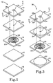
- FIG. 1 illustrates an LTCC tape structure 10 prior to lamination which includes sheets of the present ferromagnetic tape for increasing or enhancing the inductance of an inductive coil.
- the structure 10 includes LTCC tape sheets 12, 14 and 16, and ferromagnetic tape sheets 18 and 20 which are sandwiched on opposite sides of the sheet 14.
- An inductor 22 is formed as a spiral coil of electrically conductive ink on the upper surface of the sheet 14. Ends 22a and 22b of the inductor 22 are connected through vias 24 and 26 which extend through the sheet 18 and vias 28 and 30 which extend through the sheet 12 to conductor pads 32 and 34 respectively which are formed on the surface of the sheet 12. Since the ferromagnetic sheets 18 and 20 have very high electrical resistivity and can be considered as insulators, the vias 24 and 26 are not shorted out by the sheet 18.
- the structure 10 is fabricated by sandwiching the elements illustrated in FIG. 1 together, laminating, prefiring and cofiring to produce the integral structure 10 as illustrated in FIG. 2.
- the sheets 18 and 20 are vertically aligned with the inductor 22, and interact with the magnetic field produced upon flow of current through the inductor 22 to increase or enhance the inductance of the inductor 22. If desired, only one of the sheets 18 and 20 may be provided with a corresponding reduction in inductance enhancement.
- FIGs. 3 and 4 illustrate a structure 36 which is similar to the structure 10 except that the ferromagnetic tape sheet 20 is replaced by a layer 20' of ferromagnetic material formed on the upper surface of the sheet 16.
- the ferromagnetic tape sheet 18 is replaced by a layer 18' of ferromagnetic material formed on the upper surface of an LTCC sheet 37.
- the layers 18' and 20' are formed by screen printing or otherwise applying ferromagnetic ink embodying the present invention on the surfaces of the sheets 37 and 16 respectively, and allowing the ink to dry to form a solid layer. It will be noted that since the ferromagnetic ink is essentially electrically insulative, the LTCC sheet 37 could be omitted and the ferromagnetic layer 18' printed over the inductor 22 on the sheet 14.
- FIGs. 5 and 6 illustrate how an LTCC structure 40 embodying the invention can be fabricated as including a magnetic shield for a component 42.
- the external interconnections of the component 42 are not shown.
- the component 42 can be an electrical metallization pattern or any other element which must be shielded from external magnetic fields.
- the component 42 is inserted in a cavity 44 formed through an LTCC sheet 46.
- a ferromagnetic layer 48 is formed of ferromagnetic ink or tape over the component 42 and surrounding portions of the sheet 46.
- Another ferromagnetic layer 50 is formed of ferromagnetic tape or ink on the surface of an LTCC sheet 52 in vertical alignment with the layer 48.
- a plurality of ferromagnetic vias 54 are formed in respective holes 56 which extend through the sheet 46.
- the vias 54 are formed by screen printing ferromagnetic ink into the holes 56 to fill or at least coat the walls of the holes 56.
- the vias 54 form a magnetic ring or fence around the component 42.
- the vias 54 extend between the layers 48 and 50 to form a magnetic circuit which provides lateral as well as vertical magnetic shielding. Further illustrated is another LTCC sheet 58 which is sandwiched above the sheet 46.
- FIG. 7 illustrates another magnetic shielding arrangement according to the present invention.
- An LTCC structure 60 includes LTCC layers 62, 64, 66, 68 and 70. Electrical conductor traces or metallizations 72 and 74 are formed on the surface of the layer 66, whereas metallizations 76, 78 and 80 are formed on the surface of the layer 68.
- Vertical magnetic shielding is provided by ferromagnetic layers 82 and 84 formed on the surfaces of the layers 64 and 70 respectively.
- Lateral magnetic shielding is provided by ferromagnetic vias 86, 88 and 90 formed through the layers 64, 66 and 68 respectively.
- the vias 88 are staggered from the vias 86 and 90 to prevent excessive local material thickness and weakness. Although the vias described and illustrated thus far have circular cross-sections, it is within the scope of the invention to form ferromagnetic vias with linear, arcuate or other cross-sections.
- FIGs. 8 and 9 illustrate another LTCC structure 100 embodying the present invention prior to lamination and after cofiring respectively.
- the structure 100 includes LTCC sheets 102, 104, 106, 108 and 110.
- Vertically aligned holes 104a, 106a and 108a are formed through the sheets 104, 106 and 108 respectively to form a cavity 112 as illustrated in FIG. 9.
- a drop-in component 114 which can be an inductor, thermistor, capacitor, varistor, ferromagnetic core or other element has a shape corresponding to the cavity 112 and is inserted therein during assembly.
- the component 114 is made of a material or materials which are cofirable with LTCC tape.
- the component 114 can be fired prior to assembly in the structure 100, or can be cofired (for sintering) with the LTCC tape sheets.
- conductor layers 116 and 118 which extend from the opposite lateral ends of the conductor 114 over the upper edge thereof, and vias 120 and 122 which extend through the sheet 102 for connection to conductor pads 124 and 126 respectively.
- FIG. 10 illustrates another LTCC structure 130 in which a drop-in component is mounted in a cavity 132 formed through only the upper layers of the structure 130. More specifically, the structure 130 includes LTCC sheets 134, 136, 138 and 140. The cavity 132 extends through only the sheets 134 and 136.
- the drop-in component is a capacitor 142 including a dielectric layer 144 which is sandwiched between conductor layers 146 and 148.
- a conductor layer 150 extends from the layer 146 downwardly around the left end and wraps around a portion of the lower surface of the dielectric layer 144.
- the conductor 148 is omitted in this area to prevent shorting of the layer 150 to the layer 148.
- the conductor layer 148 is connected to a buried metallization 152 formed on the sheet 140 by a via 154 which extends through the sheet 138 and a solder connection 156.
- the conductor layer 150 is connected to a buried metallization 158 formed on the sheet 140 by a via 160 which extends through the sheet 138 and a solder connection 162.
- a drop-in component made of a non-magnetic material into an LTCC structure 170 which includes LTCC tape sheets 172, 174 and 176.
- a cavity 178 extends through all of the sheets 172, 174 and 176.
- a component, such as a microelectronic integrated circuit chip 180, is mounted on the structure 170 above the cavity 178 by a thermally conductive adhesive 181.
- An integral heat sink 182 made of aluminum or other thermally conductive material, includes a planar base portion 184, and a vertical portion 186 which extends upwardly from the base portion 184 through the cavity 178 into thermal contact with the component 180. Heat generated by the component 180 is conducted to the base portion 184 of the heat sink 182 through the vertical portion 186 thereof and dissipated into the atmosphere.
- the structure 170 is fabricated by assembling the LTCC sheets 172, 174 and 176 onto the heat sink 182, laminating, prefiring and cofiring. Although not specifically illustrated, it is further within the scope to fully or partially bury the component 180 in the sheets 172, 174 and 178.
- a metallization 188 which is formed on the sheet 174 and connected to the component 180 by a via 190, bonding pad 192, wire bond 194 and bonding pad 196.
- a metallization 198 is formed on the sheet 176 and connected to the component 180 by vias 200 and 202, a bonding pad 204, wire bond 206 and bonding pad 208.
- FIGs. 12 to 14 illustrate an LTCC transformer structure 250 embodying the present invention, including LTCC tape sheets 252, 254, 256, 258 and 260 which are formed with central circular holes 252a, 254a, 256a, 258a and 260a respectively.
- Three electrical conductors in the shape of concentric circular arcs are formed on each of the sheets 254, 256 and 258. More specifically, radially outer conductors 254b, 256b and 258b, radially central conductors 254c, 256c and 258c and radially inner conductors 254d, 256d and 258d are formed on the sheets 254, 256 and 258 respectively.
- Each of the conductors has a gap as illustrated.
- the ends of the conductors on adjacent sheets are interconnected by vias which are not illustrated explicitly, but indicated by arrows.
- the outer conductors 254b, 256b and 258b are interconnected by vias to constitute a first section of a primary winding through which current flows downwardly.
- the inner conductors 254d, 256d and 258d are interconnected by vias to constitute a second section of the primary winding through which current flows upwardly.
- the first and second sections of the primary winding are interconnected to form a continuous electrical current path which generates additive magnetic fields.
- the central conductors 254c, 256c and 258c are interconnected to constitute a secondary winding through which current flows downwardly. Current flows counterclockwise through all of the conductors.
- the via 270 is connected to a via 272 by a metallization 274 formed on the sheet 260.
- Current flows upwardly through the via 272, through the conductor 258d, upwardly through a via 276, through the conductor 256d, upwardly through a via 278, through the conductor 254d and upwardly through a via 280 to a bonding pad 282.
- the magnetic field induced in the secondary winding from the primary winding flows into a bonding pad 284 and downwardly through a via 286, through the conductor 254c, downwardly through a via 288, through the conductor 256c, downwardly through a via 290, through the conductor 258c and downwardly through a via 292 to a metallization 294 formed on the sheet 260.
- the transformer structure 250 provides a voltage step-down ratio of 1:2, since the primary winding has twice as many turns as the secondary winding. It is of course possible to operate the transformer structure 250 in reverse, in which case the primary winding would include the central conductors and the secondary winding would include the inner and outer conductors. In this case, the primary winding would have half as many turns as the second winding, and the structure 250 would provide a voltage step-up ratio of 2:1. It is further within the scope of the invention, although not specifically illustrated, to provide two or more primary windings and/or two or more secondary windings.
- the transformer structure 250 further comprises a central core 300 formed of a ferromagnetic material which extends through the holes 252a, 254a, 256a, 258a and 260a.
- the core 300 is assembled and cofired with the sheets 252, 254, 256, 258 and 260 as described above.
- the structure 250 may further include a C-core 302 which engages with the ends of the central core 300 and forms a complete magnetic circuit therewith.
Landscapes
- Engineering & Computer Science (AREA)
- Microelectronics & Electronic Packaging (AREA)
- Coils Or Transformers For Communication (AREA)
- Glass Compositions (AREA)
- Soft Magnetic Materials (AREA)
- Production Of Multi-Layered Print Wiring Board (AREA)
- Shielding Devices Or Components To Electric Or Magnetic Fields (AREA)
- Compositions Of Oxide Ceramics (AREA)
Applications Claiming Priority (2)
| Application Number | Priority Date | Filing Date | Title |
|---|---|---|---|
| US923409 | 1992-07-31 | ||
| US07/923,409 US5312674A (en) | 1992-07-31 | 1992-07-31 | Low-temperature-cofired-ceramic (LTCC) tape structures including cofired ferromagnetic elements, drop-in components and multi-layer transformer |
Publications (3)
| Publication Number | Publication Date |
|---|---|
| EP0581206A2 true EP0581206A2 (de) | 1994-02-02 |
| EP0581206A3 EP0581206A3 (en) | 1997-10-01 |
| EP0581206B1 EP0581206B1 (de) | 2003-01-02 |
Family
ID=25448646
Family Applications (1)
| Application Number | Title | Priority Date | Filing Date |
|---|---|---|---|
| EP93111808A Expired - Lifetime EP0581206B1 (de) | 1992-07-31 | 1993-07-23 | Bei niedriger Temperatur gesinterte keramische Bandstruktur mit gleichzeitig gesintertem ferromagnetischen Element |
Country Status (4)
| Country | Link |
|---|---|
| US (2) | US5312674A (de) |
| EP (1) | EP0581206B1 (de) |
| JP (1) | JPH06216538A (de) |
| DE (1) | DE69332599T2 (de) |
Cited By (14)
| Publication number | Priority date | Publication date | Assignee | Title |
|---|---|---|---|---|
| EP0674354A3 (de) * | 1994-03-24 | 1996-07-17 | Hochiki Co | Drahtloses Zugangskontrollsystem mit Annäherungselement unt Antenneneinrichtung hierfür. |
| EP0786927A1 (de) * | 1996-01-25 | 1997-07-30 | Murata Manufacturing Co., Ltd. | Komposit funktionelles Gerät und ihr Herstellungsverfahren |
| WO1999005786A1 (en) * | 1997-07-22 | 1999-02-04 | Avx Corporation | Multilayer ceramic rc device |
| EP0901316A3 (de) * | 1997-09-08 | 2000-11-22 | Murata Manufacturing Co., Ltd. | Mehrschichtiges keramisches Substrat und Verfahren zur Herstellung des mehrschichtigen keramischen Substrats |
| EP1113710A1 (de) * | 1999-12-27 | 2001-07-04 | Tridonic Bauelemente GmbH | Eledtronisches Vorschaltgerät zum Betrieb einer Niederdruckentladungslampe |
| WO2001049083A1 (de) * | 1999-12-27 | 2001-07-05 | Tridonicatco Gmbh & Co. Kg | Elektronisches vorschaltgerät und elektronischer transformator |
| US6525628B1 (en) | 1999-06-18 | 2003-02-25 | Avx Corporation | Surface mount RC array with narrow tab portions on each of the electrode plates |
| US6747420B2 (en) | 2000-03-17 | 2004-06-08 | Tridonicatco Gmbh & Co. Kg | Drive circuit for light-emitting diodes |
| US6826059B2 (en) | 2000-03-17 | 2004-11-30 | Tridonicatco Gmbh & Co. Kg | Drive for light-emitting diodes |
| CN103906352A (zh) * | 2014-04-07 | 2014-07-02 | 深圳市力磁电子有限公司 | 厚膜导电合成材料及制备多层电路的方法 |
| WO2015176919A1 (de) * | 2014-05-23 | 2015-11-26 | Siemens Aktiengesellschaft | Mehrlagiges induktives passives bauelement und folienkörper zu dessen herstellung |
| WO2016026476A1 (de) * | 2014-08-22 | 2016-02-25 | Balluff Gmbh | Induktiver näherungssensor in integrierter bauweise |
| EP3964038A4 (de) * | 2019-05-02 | 2022-11-02 | Nano-Dimension Technologies, Ltd. | Systeme und verfahren zur herstellung von spulen für kernlose transformatoren und induktoren |
| US12471217B2 (en) | 2019-05-02 | 2025-11-11 | Nano Dimension Technologies, Ltd. | Systems and methods of fabricating coils for coreless transformers and inductors |
Families Citing this family (174)
| Publication number | Priority date | Publication date | Assignee | Title |
|---|---|---|---|---|
| WO1994007349A1 (en) * | 1992-09-24 | 1994-03-31 | Hughes Aircraft Company | Magnetic vias within multi-layer, 3-dimensional structures/substrates |
| US5410289A (en) * | 1993-10-12 | 1995-04-25 | Delta Star Electric, Inc. | Electromagnet |
| US6911887B1 (en) * | 1994-09-12 | 2005-06-28 | Matsushita Electric Industrial Co., Ltd. | Inductor and method for producing the same |
| US5726621A (en) * | 1994-09-12 | 1998-03-10 | Cooper Industries, Inc. | Ceramic chip fuses with multiple current carrying elements and a method for making the same |
| KR100231356B1 (ko) | 1994-09-12 | 1999-11-15 | 모리시타요이찌 | 적층형 세라믹칩 인덕터 및 그 제조방법 |
| US5990776A (en) * | 1994-12-08 | 1999-11-23 | Jitaru; Ionel | Low noise full integrated multilayers magnetic for power converters |
| US5821846A (en) * | 1995-05-22 | 1998-10-13 | Steward, Inc. | High current ferrite electromagnetic interference suppressor and associated method |
| US5661647A (en) * | 1995-06-07 | 1997-08-26 | Hughes Electronics | Low temperature co-fired ceramic UHF/VHF power converters |
| US5781091A (en) * | 1995-07-24 | 1998-07-14 | Autosplice Systems Inc. | Electronic inductive device and method for manufacturing |
| US5849355A (en) * | 1996-09-18 | 1998-12-15 | Alliedsignal Inc. | Electroless copper plating |
| US5777539A (en) * | 1995-09-27 | 1998-07-07 | International Business Machines Corporation | Inductor using multilayered printed circuit board for windings |
| US5609946A (en) * | 1995-10-03 | 1997-03-11 | General Electric Company | High frequency, high density, low profile, magnetic circuit components |
| US5757611A (en) * | 1996-04-12 | 1998-05-26 | Norhtrop Grumman Corporation | Electronic package having buried passive components |
| US5877667A (en) * | 1996-08-01 | 1999-03-02 | Advanced Micro Devices, Inc. | On-chip transformers |
| US5762388A (en) * | 1996-08-08 | 1998-06-09 | Carlton G. Smith | Grapple |
| US6168219B1 (en) * | 1996-08-08 | 2001-01-02 | David M. Futa | Grapple |
| DE19636742C2 (de) * | 1996-09-10 | 1999-05-12 | Siemens Matsushita Components | Einrichtung zur Einstellung eines definierten elektrischen Potentials auf einem Ferritkern eines induktiven Bauelementes und/oder zur Verringerung einer Bedämpfung des induktiven Bauelementes durch von dessen Magnetfeld induzierte Wirbelströme |
| US5801108A (en) * | 1996-09-11 | 1998-09-01 | Motorola Inc. | Low temperature cofireable dielectric paste |
| DE19637211C2 (de) * | 1996-09-12 | 1999-06-24 | Siemens Matsushita Components | Einrichtung zur Abführung von Wärme von Ferritkernen induktiver Bauelemente |
| JP3077056B2 (ja) * | 1996-09-12 | 2000-08-14 | 株式会社村田製作所 | 積層型電子部品 |
| JP3097569B2 (ja) * | 1996-09-17 | 2000-10-10 | 株式会社村田製作所 | 積層チップインダクタの製造方法 |
| US6073339A (en) * | 1996-09-20 | 2000-06-13 | Tdk Corporation Of America | Method of making low profile pin-less planar magnetic devices |
| TW342506B (en) * | 1996-10-11 | 1998-10-11 | Matsushita Electric Industrial Co Ltd | Inductance device and wireless terminal equipment |
| JP3513787B2 (ja) * | 1996-11-18 | 2004-03-31 | 株式会社村田製作所 | Lc複合部品 |
| US5795422A (en) * | 1997-01-02 | 1998-08-18 | Eastman Kodak Company | Method for forming molded ceramic devices having embedded spiral coils |
| JP2001513697A (ja) | 1997-02-24 | 2001-09-04 | スーペリア マイクロパウダーズ リミテッド ライアビリティ カンパニー | エアロゾル法及び装置、粒子製品、並びに該粒子製品から製造される電子装置 |
| US6111520A (en) * | 1997-04-18 | 2000-08-29 | Georgia Tech Research Corp. | System and method for the wireless sensing of physical properties |
| US5783879A (en) * | 1997-06-03 | 1998-07-21 | Eastman Kodak Company | Micromotor in a ceramic substrate |
| US6118351A (en) * | 1997-06-10 | 2000-09-12 | Lucent Technologies Inc. | Micromagnetic device for power processing applications and method of manufacture therefor |
| US6440750B1 (en) | 1997-06-10 | 2002-08-27 | Agere Systems Guardian Corporation | Method of making integrated circuit having a micromagnetic device |
| US6191495B1 (en) * | 1997-06-10 | 2001-02-20 | Lucent Technologies Inc. | Micromagnetic device having an anisotropic ferromagnetic core and method of manufacture therefor |
| JPH11154805A (ja) * | 1997-09-22 | 1999-06-08 | Tdk Corp | 積層セラミック部品 |
| TW388889B (en) * | 1997-12-17 | 2000-05-01 | Koninkl Philips Electronics Nv | Planar transformer |
| US6169801B1 (en) | 1998-03-16 | 2001-01-02 | Midcom, Inc. | Digital isolation apparatus and method |
| US6278379B1 (en) * | 1998-04-02 | 2001-08-21 | Georgia Tech Research Corporation | System, method, and sensors for sensing physical properties |
| US6127296A (en) * | 1998-04-24 | 2000-10-03 | Tdk Corporation | Ceramic-glass composite material and method for the preparation thereof |
| DE19820234A1 (de) * | 1998-05-06 | 1999-11-11 | Giesecke & Devrient Gmbh | Anordnung zur Übertragung von Signalen zwischen einem Bauelement eines tragbaren Datenträgers und einer dem Bauelement fest zugeordneten Zuleitung |
| US6054914A (en) * | 1998-07-06 | 2000-04-25 | Midcom, Inc. | Multi-layer transformer having electrical connection in a magnetic core |
| US20030148024A1 (en) * | 2001-10-05 | 2003-08-07 | Kodas Toivo T. | Low viscosity precursor compositons and methods for the depositon of conductive electronic features |
| US6191934B1 (en) * | 1998-10-02 | 2001-02-20 | Sarnoff Corporation & Co., Ltd. | High dielectric constant embedded capacitors |
| US6572830B1 (en) | 1998-10-09 | 2003-06-03 | Motorola, Inc. | Integrated multilayered microfludic devices and methods for making the same |
| US6592696B1 (en) | 1998-10-09 | 2003-07-15 | Motorola, Inc. | Method for fabricating a multilayered structure and the structures formed by the method |
| US6303423B1 (en) * | 1998-12-21 | 2001-10-16 | Megic Corporation | Method for forming high performance system-on-chip using post passivation process |
| US6198374B1 (en) | 1999-04-01 | 2001-03-06 | Midcom, Inc. | Multi-layer transformer apparatus and method |
| CN1178232C (zh) | 1999-04-26 | 2004-12-01 | 松下电器产业株式会社 | 电子零件及无线终端装置 |
| US6255714B1 (en) | 1999-06-22 | 2001-07-03 | Agere Systems Guardian Corporation | Integrated circuit having a micromagnetic device including a ferromagnetic core and method of manufacture therefor |
| US6278352B1 (en) * | 1999-07-26 | 2001-08-21 | Taiwan Semiconductor Manufacturing Company | High efficiency thin film inductor |
| US6639508B1 (en) | 1999-09-22 | 2003-10-28 | Aptek Williams, Inc. | Electrical switch device and process for manufacturing same |
| DE19963290B4 (de) * | 1999-12-27 | 2011-07-21 | Tridonic Gmbh & Co Kg | Planare Induktivität |
| US6198393B1 (en) * | 2000-02-07 | 2001-03-06 | Westvaco Corporation | Foil/ink composite inductor |
| JP2001244123A (ja) * | 2000-02-28 | 2001-09-07 | Kawatetsu Mining Co Ltd | 表面実装型平面磁気素子及びその製造方法 |
| US6674355B2 (en) * | 2000-05-19 | 2004-01-06 | M-Flex Multi-Fineline Electronix, Inc. | Slot core transformers |
| US6538307B1 (en) * | 2000-06-28 | 2003-03-25 | Advanced Micro Devices, Inc. | Packaging substrate comprising staggered vias |
| TWI258154B (en) * | 2000-09-22 | 2006-07-11 | Flex Multi Fineline Electronix | Electronic transformer/inductor devices and methods for making same |
| US6794320B1 (en) * | 2000-12-15 | 2004-09-21 | Sciperio, Inc. | Direction in low-temperature paste development |
| US20030112110A1 (en) * | 2001-09-19 | 2003-06-19 | Mark Pavier | Embedded inductor for semiconductor device circuit |
| US6743534B2 (en) | 2001-10-01 | 2004-06-01 | Heraeus Incorporated | Self-constrained low temperature glass-ceramic unfired tape for microelectronics and methods for making and using the same |
| US7524528B2 (en) * | 2001-10-05 | 2009-04-28 | Cabot Corporation | Precursor compositions and methods for the deposition of passive electrical components on a substrate |
| US7629017B2 (en) * | 2001-10-05 | 2009-12-08 | Cabot Corporation | Methods for the deposition of conductive electronic features |
| US20030108664A1 (en) * | 2001-10-05 | 2003-06-12 | Kodas Toivo T. | Methods and compositions for the formation of recessed electrical features on a substrate |
| US6951666B2 (en) * | 2001-10-05 | 2005-10-04 | Cabot Corporation | Precursor compositions for the deposition of electrically conductive features |
| US20060159838A1 (en) * | 2005-01-14 | 2006-07-20 | Cabot Corporation | Controlling ink migration during the formation of printable electronic features |
| JP4763237B2 (ja) | 2001-10-19 | 2011-08-31 | キャボット コーポレイション | 基板上に導電性電子部品を製造する方法 |
| US7553512B2 (en) * | 2001-11-02 | 2009-06-30 | Cabot Corporation | Method for fabricating an inorganic resistor |
| US6914513B1 (en) | 2001-11-08 | 2005-07-05 | Electro-Science Laboratories, Inc. | Materials system for low cost, non wire-wound, miniature, multilayer magnetic circuit components |
| US6844789B2 (en) * | 2001-11-13 | 2005-01-18 | Raytheon Company | Low temperature co-fired ceramic (LTCC) circulator |
| US6778043B2 (en) * | 2001-12-19 | 2004-08-17 | Maxxan Systems, Inc. | Method and apparatus for adding inductance to printed circuits |
| SE0200404D0 (sv) * | 2002-02-11 | 2002-02-11 | Saab Ab | Microwave component |
| US6806790B2 (en) * | 2002-02-19 | 2004-10-19 | Scientific Components, Inc. | Miniature 180 degree power splitter |
| US6686812B2 (en) * | 2002-05-22 | 2004-02-03 | Honeywell International Inc. | Miniature directional coupler |
| WO2003100799A1 (en) * | 2002-05-24 | 2003-12-04 | Philips Intellectual Property & Standards Gmbh | Hybrid electronic device comprising a low-temperature-cofired-ceramic ltcc-tape |
| US6900708B2 (en) * | 2002-06-26 | 2005-05-31 | Georgia Tech Research Corporation | Integrated passive devices fabricated utilizing multi-layer, organic laminates |
| US7260890B2 (en) * | 2002-06-26 | 2007-08-28 | Georgia Tech Research Corporation | Methods for fabricating three-dimensional all organic interconnect structures |
| US6987307B2 (en) * | 2002-06-26 | 2006-01-17 | Georgia Tech Research Corporation | Stand-alone organic-based passive devices |
| US7135952B2 (en) | 2002-09-16 | 2006-11-14 | Multi-Fineline Electronix, Inc. | Electronic transformer/inductor devices and methods for making same |
| KR100735208B1 (ko) * | 2002-10-23 | 2007-07-03 | 내슨테크날러지 인코포레이티드 | 자심 내에 전기 연결을 포함하는 다층 변압기 |
| US6927661B2 (en) * | 2003-03-05 | 2005-08-09 | Tdk Innoveta Inc. | Planar transformer and output inductor structure with single planar winding board and two magnetic cores |
| US7489914B2 (en) * | 2003-03-28 | 2009-02-10 | Georgia Tech Research Corporation | Multi-band RF transceiver with passive reuse in organic substrates |
| US8026729B2 (en) | 2003-09-16 | 2011-09-27 | Cardiomems, Inc. | System and apparatus for in-vivo assessment of relative position of an implant |
| WO2005027998A2 (en) | 2003-09-16 | 2005-03-31 | Cardiomems, Inc. | Implantable wireless sensor |
| US20050104158A1 (en) * | 2003-11-19 | 2005-05-19 | Scintera Networks, Inc. | Compact, high q inductor for integrated circuit |
| JP4464127B2 (ja) * | 2003-12-22 | 2010-05-19 | Necエレクトロニクス株式会社 | 半導体集積回路及びその製造方法 |
| DE102004014752B4 (de) * | 2004-03-25 | 2008-11-20 | Infineon Technologies Ag | Halbleiterbauelement mit kernlosem Wandler und Halbbrücke |
| US7180315B2 (en) * | 2004-06-28 | 2007-02-20 | Sv Probe, Ltd. | Substrate with patterned conductive layer |
| US8345433B2 (en) * | 2004-07-08 | 2013-01-01 | Avx Corporation | Heterogeneous organic laminate stack ups for high frequency applications |
| US7436282B2 (en) * | 2004-12-07 | 2008-10-14 | Multi-Fineline Electronix, Inc. | Miniature circuitry and inductive components and methods for manufacturing same |
| EP1861857A4 (de) * | 2004-12-07 | 2009-09-02 | Multi Fineline Electronix Inc | Miniaturschaltkreise und induktive komponenten und herstellungsverfahren dafür |
| US20060190917A1 (en) * | 2005-01-14 | 2006-08-24 | Cabot Corporation | System and process for manufacturing application specific printable circuits (ASPC'S) and other custom electronic devices |
| WO2006076608A2 (en) * | 2005-01-14 | 2006-07-20 | Cabot Corporation | A system and process for manufacturing custom electronics by combining traditional electronics with printable electronics |
| AU2006204813A1 (en) * | 2005-01-14 | 2006-07-20 | Cabot Corporation | Security features, their use, and processes for making them |
| US20060163744A1 (en) * | 2005-01-14 | 2006-07-27 | Cabot Corporation | Printable electrical conductors |
| US20060158497A1 (en) * | 2005-01-14 | 2006-07-20 | Karel Vanheusden | Ink-jet printing of compositionally non-uniform features |
| WO2006076606A2 (en) | 2005-01-14 | 2006-07-20 | Cabot Corporation | Optimized multi-layer printing of electronics and displays |
| WO2006076609A2 (en) | 2005-01-14 | 2006-07-20 | Cabot Corporation | Printable electronic features on non-uniform substrate and processes for making same |
| US8383014B2 (en) | 2010-06-15 | 2013-02-26 | Cabot Corporation | Metal nanoparticle compositions |
| TW200640596A (en) * | 2005-01-14 | 2006-12-01 | Cabot Corp | Production of metal nanoparticles |
| US7824466B2 (en) | 2005-01-14 | 2010-11-02 | Cabot Corporation | Production of metal nanoparticles |
| AU2006262287A1 (en) * | 2005-06-21 | 2007-01-04 | Cardiomems, Inc. | Method of manufacturing implantable wireless sensor for in vivo pressure measurement |
| DE102005037950B3 (de) * | 2005-08-11 | 2007-04-19 | Imst Gmbh | Ein Verfahren zum vereinfachten Aufbau von Mikrowellenschaltungen in LTCC-Technik mit reduzierter Anzahl von Durchgangslöchern |
| US7638988B2 (en) * | 2006-02-21 | 2009-12-29 | Virginia Tech Intellectual Properties, Inc. | Co-fired ceramic inductors with variable inductance, and voltage regulator having same |
| US7932800B2 (en) * | 2006-02-21 | 2011-04-26 | Virginia Tech Intellectual Properties, Inc. | Method and apparatus for three-dimensional integration of embedded power module |
| US7645941B2 (en) | 2006-05-02 | 2010-01-12 | Multi-Fineline Electronix, Inc. | Shielded flexible circuits and methods for manufacturing same |
| US7625637B2 (en) * | 2006-05-31 | 2009-12-01 | Cabot Corporation | Production of metal nanoparticles from precursors having low reduction potentials |
| US7439840B2 (en) | 2006-06-27 | 2008-10-21 | Jacket Micro Devices, Inc. | Methods and apparatuses for high-performing multi-layer inductors |
| US7340825B2 (en) * | 2006-07-06 | 2008-03-11 | Harris Corporation | Method of making a transformer |
| US7449987B2 (en) | 2006-07-06 | 2008-11-11 | Harris Corporation | Transformer and associated method of making |
| US8521303B2 (en) * | 2006-07-17 | 2013-08-27 | University Of Utah Reasearch Foundation | In vivo implantable coil assembly |
| US7808434B2 (en) * | 2006-08-09 | 2010-10-05 | Avx Corporation | Systems and methods for integrated antennae structures in multilayer organic-based printed circuit devices |
| US8061017B2 (en) * | 2006-08-28 | 2011-11-22 | Avago Technologies Ecbu Ip (Singapore) Pte. Ltd. | Methods of making coil transducers |
| US20080278275A1 (en) * | 2007-05-10 | 2008-11-13 | Fouquet Julie E | Miniature Transformers Adapted for use in Galvanic Isolators and the Like |
| US7852186B2 (en) * | 2006-08-28 | 2010-12-14 | Avago Technologies Ecbu Ip (Singapore) Pte. Ltd. | Coil transducer with reduced arcing and improved high voltage breakdown performance characteristics |
| US7791900B2 (en) | 2006-08-28 | 2010-09-07 | Avago Technologies General Ip (Singapore) Pte. Ltd. | Galvanic isolator |
| US8385043B2 (en) * | 2006-08-28 | 2013-02-26 | Avago Technologies ECBU IP (Singapoare) Pte. Ltd. | Galvanic isolator |
| US8093983B2 (en) * | 2006-08-28 | 2012-01-10 | Avago Technologies Ecbu Ip (Singapore) Pte. Ltd. | Narrowbody coil isolator |
| US8427844B2 (en) * | 2006-08-28 | 2013-04-23 | Avago Technologies Ecbu Ip (Singapore) Pte. Ltd. | Widebody coil isolators |
| US7948067B2 (en) * | 2009-06-30 | 2011-05-24 | Avago Technologies Ecbu Ip (Singapore) Pte. Ltd. | Coil transducer isolator packages |
| US9105391B2 (en) * | 2006-08-28 | 2015-08-11 | Avago Technologies General Ip (Singapore) Pte. Ltd. | High voltage hold-off coil transducer |
| US9019057B2 (en) * | 2006-08-28 | 2015-04-28 | Avago Technologies General Ip (Singapore) Pte. Ltd. | Galvanic isolators and coil transducers |
| US9589716B2 (en) | 2006-09-12 | 2017-03-07 | Cooper Technologies Company | Laminated magnetic component and manufacture with soft magnetic powder polymer composite sheets |
| US8941457B2 (en) | 2006-09-12 | 2015-01-27 | Cooper Technologies Company | Miniature power inductor and methods of manufacture |
| US8466764B2 (en) * | 2006-09-12 | 2013-06-18 | Cooper Technologies Company | Low profile layered coil and cores for magnetic components |
| US8378777B2 (en) | 2008-07-29 | 2013-02-19 | Cooper Technologies Company | Magnetic electrical device |
| US8310332B2 (en) * | 2008-10-08 | 2012-11-13 | Cooper Technologies Company | High current amorphous powder core inductor |
| US7791445B2 (en) * | 2006-09-12 | 2010-09-07 | Cooper Technologies Company | Low profile layered coil and cores for magnetic components |
| US7989895B2 (en) * | 2006-11-15 | 2011-08-02 | Avx Corporation | Integration using package stacking with multi-layer organic substrates |
| US20080186123A1 (en) * | 2007-02-07 | 2008-08-07 | Industrial Technology Research Institute | Inductor devices |
| US8258911B2 (en) | 2008-03-31 | 2012-09-04 | Avago Technologies ECBU IP (Singapor) Pte. Ltd. | Compact power transformer components, devices, systems and methods |
| TW200952301A (en) * | 2008-06-02 | 2009-12-16 | Inpaq Technology Co Ltd | Electro-static discharge protection device with low temperature co-fire ceramic and manufacturing method thereof |
| US9558881B2 (en) | 2008-07-11 | 2017-01-31 | Cooper Technologies Company | High current power inductor |
| US8659379B2 (en) | 2008-07-11 | 2014-02-25 | Cooper Technologies Company | Magnetic components and methods of manufacturing the same |
| US8279037B2 (en) * | 2008-07-11 | 2012-10-02 | Cooper Technologies Company | Magnetic components and methods of manufacturing the same |
| US9859043B2 (en) | 2008-07-11 | 2018-01-02 | Cooper Technologies Company | Magnetic components and methods of manufacturing the same |
| US20100277267A1 (en) * | 2009-05-04 | 2010-11-04 | Robert James Bogert | Magnetic components and methods of manufacturing the same |
| US8089331B2 (en) * | 2009-05-12 | 2012-01-03 | Raytheon Company | Planar magnetic structure |
| US20100303733A1 (en) * | 2009-05-29 | 2010-12-02 | Searete Llc, A Limited Liability Corporation Of The State Of Delaware | Systems, devices, methods, and compositions including ferromagnetic structures |
| US8154285B1 (en) | 2009-05-29 | 2012-04-10 | The Invention Science Fund I, Llc | Non-external static magnetic field imaging systems, devices, methods, and compositions |
| US8058872B2 (en) | 2009-05-29 | 2011-11-15 | The Invention Science Fund I, Llc | Systems, devices, methods, and compositions including functionalized ferromagnetic structures |
| US8063636B2 (en) * | 2009-05-29 | 2011-11-22 | The Invention Science Fund I, Llc | Systems, devices, methods, and compositions including targeted ferromagnetic structures |
| US8106655B2 (en) * | 2009-05-29 | 2012-01-31 | The Invention Science Fund I, Llc | Multiplex imaging systems, devices, methods, and compositions including ferromagnetic structures |
| KR101215303B1 (ko) * | 2009-07-21 | 2012-12-26 | 한국전자통신연구원 | 엘티씨씨 인덕터를 포함하는 전자 장치 |
| JP5110178B2 (ja) * | 2010-04-13 | 2012-12-26 | 株式会社デンソー | 半導体装置およびその製造方法 |
| DE102010015659A1 (de) * | 2010-04-20 | 2011-10-20 | Giesecke & Devrient Gmbh | Transferverfahren zur Herstellung von Leiterstrukturen mittels Nanotinten |
| WO2012111203A1 (ja) * | 2011-02-15 | 2012-08-23 | 株式会社村田製作所 | 積層型インダクタ素子 |
| ITTO20110295A1 (it) * | 2011-04-01 | 2012-10-02 | St Microelectronics Srl | Dispositivo ad induttore integrato ad elevato valore di induttanza, in particolare per l'uso come antenna in un sistema di identificazione a radiofrequenza |
| JP6283158B2 (ja) * | 2012-04-12 | 2018-02-21 | 新光電気工業株式会社 | 配線基板、及び、配線基板の製造方法 |
| US9691538B1 (en) * | 2012-08-30 | 2017-06-27 | Volterra Semiconductor LLC | Magnetic devices for power converters with light load enhancers |
| DE102013100622B4 (de) * | 2013-01-22 | 2018-03-01 | Phoenix Contact Gmbh & Co. Kg | Leiterplatte im Lagenaufbau |
| KR20150090445A (ko) | 2014-01-29 | 2015-08-06 | 주식회사 이노칩테크놀로지 | 적층칩 소자 |
| US10665377B2 (en) * | 2014-05-05 | 2020-05-26 | 3D Glass Solutions, Inc. | 2D and 3D inductors antenna and transformers fabricating photoactive substrates |
| US9520793B2 (en) | 2014-09-22 | 2016-12-13 | Raytheon Company | Stacked power converter assembly |
| JP6233285B2 (ja) * | 2014-11-28 | 2017-11-22 | 三菱電機株式会社 | 半導体モジュール、電力変換装置 |
| US10050438B2 (en) | 2015-10-16 | 2018-08-14 | Raytheon Company | Stacked power converter assembly |
| US10049810B2 (en) | 2015-11-09 | 2018-08-14 | Raytheon Company | High voltage high frequency transformer |
| US10497506B2 (en) * | 2015-12-18 | 2019-12-03 | Texas Instruments Incorporated | Methods and apparatus for isolation barrier with integrated magnetics for high power modules |
| US10641508B2 (en) * | 2016-02-12 | 2020-05-05 | Goodman Manufacturing Company LP | Systems and methods for air temperature control using a target time based control plan |
| US10340577B2 (en) | 2016-02-17 | 2019-07-02 | Eagantu Ltd. | Wide band directional coupler |
| US12165809B2 (en) | 2016-02-25 | 2024-12-10 | 3D Glass Solutions, Inc. | 3D capacitor and capacitor array fabricating photoactive substrates |
| WO2017184352A1 (en) | 2016-04-18 | 2017-10-26 | Eagantu Ltd. | A wide band radio frequency circulator |
| US10050533B2 (en) | 2016-07-26 | 2018-08-14 | Raytheon Company | High voltage high frequency transformer |
| US10770225B2 (en) * | 2016-08-08 | 2020-09-08 | Hamilton Sundstrand Corporation | Multilayered coils |
| US10741327B2 (en) | 2017-01-30 | 2020-08-11 | International Business Machines Corporation | Inductors in BEOL with particulate magnetic cores |
| US10672553B2 (en) | 2017-05-10 | 2020-06-02 | Raytheon Company | High voltage high frequency transformer |
| US20190109061A1 (en) | 2017-10-11 | 2019-04-11 | Texas Instruments Incorporated | Edge Bend for Isolation Packages |
| CN109872869B (zh) * | 2017-12-04 | 2021-12-28 | 万国半导体(开曼)股份有限公司 | 一种隔离耦合结构 |
| US10854946B2 (en) | 2017-12-15 | 2020-12-01 | 3D Glass Solutions, Inc. | Coupled transmission line resonate RF filter |
| CN109545532A (zh) * | 2018-11-23 | 2019-03-29 | 深圳顺络电子股份有限公司 | 一种基于ltcc的平面变压器及其制作方法 |
| RU2706418C2 (ru) * | 2018-12-21 | 2019-11-19 | Общество с ограниченной ответственностью "АЕДОН" | Трехмерная электронная сборка |
| US12176285B2 (en) | 2018-12-31 | 2024-12-24 | Texas Instruments Incorporated | Transformer guard trace |
| US11694832B2 (en) | 2019-02-01 | 2023-07-04 | Raytheon Company | High voltage high frequency transformer |
| US11538766B2 (en) | 2019-02-26 | 2022-12-27 | Texas Instruments Incorporated | Isolated transformer with integrated shield topology for reduced EMI |
| KR20210147040A (ko) | 2019-04-05 | 2021-12-06 | 3디 글래스 솔루션즈 인코포레이티드 | 유리 기반의 빈 기판 집적 도파관 디바이스 |
| JP2023516817A (ja) | 2020-04-17 | 2023-04-20 | スリーディー グラス ソリューションズ,インク | 広帯域誘導 |
| US20250098062A1 (en) * | 2023-09-19 | 2025-03-20 | International Business Machines Corporation | Tamper-detect assemblies including heat sink covers with integrated tamper-detect circuitry |
| DE102024115204A1 (de) * | 2024-03-07 | 2025-09-11 | Tdk Electronics Ag | Additives Fertigungsverfahren, Verfahren zur Konzeption eines Bauteils und Bauteil |
Family Cites Families (25)
| Publication number | Priority date | Publication date | Assignee | Title |
|---|---|---|---|---|
| US3483499A (en) * | 1968-08-08 | 1969-12-09 | Bourns Inc | Inductive device |
| US3833872A (en) * | 1972-06-13 | 1974-09-03 | I Marcus | Microminiature monolithic ferroceramic transformer |
| US3765082A (en) * | 1972-09-20 | 1973-10-16 | San Fernando Electric Mfg | Method of making an inductor chip |
| US4117588A (en) * | 1977-01-24 | 1978-10-03 | The United States Of America As Represented By The Secretary Of The Navy | Method of manufacturing three dimensional integrated circuits |
| JPS54110424A (en) * | 1978-02-17 | 1979-08-29 | Ricoh Co Ltd | Transformer |
| JPS6050331B2 (ja) * | 1978-09-07 | 1985-11-08 | ティーディーケイ株式会社 | インダクタンス素子とその製造方法 |
| JPS6025398B2 (ja) * | 1980-12-27 | 1985-06-18 | セントラル硝子株式会社 | グレ−ズドセラミック基板 |
| US4360441A (en) * | 1981-06-25 | 1982-11-23 | Corning Glass Works | Glass-encapsulated magnetic materials and methods for making them |
| JPS5867007A (ja) * | 1981-10-19 | 1983-04-21 | Toko Inc | 積層コイル |
| JPS58151331A (ja) * | 1982-03-02 | 1983-09-08 | Fuji Elelctrochem Co Ltd | 低温焼結可能な酸化物磁性材料 |
| JPS58184710A (ja) * | 1982-04-23 | 1983-10-28 | Tdk Corp | シ−ルド型トランス |
| JPS609220U (ja) * | 1983-06-28 | 1985-01-22 | 株式会社村田製作所 | Lc複合部品 |
| US4746557A (en) * | 1985-12-09 | 1988-05-24 | Murata Manufacturing Co., Ltd. | LC composite component |
| JPS62265796A (ja) * | 1986-05-14 | 1987-11-18 | 株式会社住友金属セラミックス | セラミツク多層配線基板およびその製造法 |
| JPS6379771A (ja) * | 1986-09-22 | 1988-04-09 | 工業技術院長 | 酸化物系セラミツクス用接着剤およびその接着方法 |
| US4956114A (en) * | 1987-07-01 | 1990-09-11 | Tdk Corporation | Sintered ferrite body, chip inductor, and composite LC part |
| JPS6490512A (en) * | 1987-10-01 | 1989-04-07 | Fujitsu Ltd | Chip type transformer |
| JP2853088B2 (ja) * | 1988-04-06 | 1999-02-03 | 株式会社村田製作所 | 複合容量を有するセラミックブロック |
| JPH0287508A (ja) * | 1988-09-22 | 1990-03-28 | Toko Inc | 積層トランス |
| JPH02101715A (ja) * | 1988-10-11 | 1990-04-13 | Mitsubishi Electric Corp | チップ形複合部品 |
| JPH02128409A (ja) * | 1988-11-08 | 1990-05-16 | Murata Mfg Co Ltd | 積層セラミック基板を用いた電磁結合装置 |
| US5028473A (en) * | 1989-10-02 | 1991-07-02 | Hughes Aircraft Company | Three dimensional microcircuit structure and process for fabricating the same from ceramic tape |
| US4991283A (en) * | 1989-11-27 | 1991-02-12 | Johnson Gary W | Sensor elements in multilayer ceramic tape structures |
| JP2953140B2 (ja) * | 1991-09-20 | 1999-09-27 | 株式会社村田製作所 | トランス |
| JPH05152134A (ja) * | 1991-11-26 | 1993-06-18 | Matsushita Electric Ind Co Ltd | インダクタンス部品用グリーンシートおよびそれを用いたインダクタンス部品 |
-
1992
- 1992-07-31 US US07/923,409 patent/US5312674A/en not_active Expired - Lifetime
-
1993
- 1993-07-23 DE DE69332599T patent/DE69332599T2/de not_active Expired - Lifetime
- 1993-07-23 EP EP93111808A patent/EP0581206B1/de not_active Expired - Lifetime
- 1993-08-02 JP JP5209907A patent/JPH06216538A/ja active Pending
-
1995
- 1995-10-11 US US08/541,170 patent/US5532667A/en not_active Expired - Lifetime
Cited By (19)
| Publication number | Priority date | Publication date | Assignee | Title |
|---|---|---|---|---|
| EP0674354A3 (de) * | 1994-03-24 | 1996-07-17 | Hochiki Co | Drahtloses Zugangskontrollsystem mit Annäherungselement unt Antenneneinrichtung hierfür. |
| US5808587A (en) * | 1994-03-24 | 1998-09-15 | Hochiki Corporation | Wireless access control system using a proximity member and antenna equipment therefor |
| EP0786927A1 (de) * | 1996-01-25 | 1997-07-30 | Murata Manufacturing Co., Ltd. | Komposit funktionelles Gerät und ihr Herstellungsverfahren |
| WO1999005786A1 (en) * | 1997-07-22 | 1999-02-04 | Avx Corporation | Multilayer ceramic rc device |
| US5889445A (en) * | 1997-07-22 | 1999-03-30 | Avx Corporation | Multilayer ceramic RC device |
| EP0901316A3 (de) * | 1997-09-08 | 2000-11-22 | Murata Manufacturing Co., Ltd. | Mehrschichtiges keramisches Substrat und Verfahren zur Herstellung des mehrschichtigen keramischen Substrats |
| US6241838B1 (en) | 1997-09-08 | 2001-06-05 | Murata Manufacturing Co., Ltd. | Method of producing a multi-layer ceramic substrate |
| US6525628B1 (en) | 1999-06-18 | 2003-02-25 | Avx Corporation | Surface mount RC array with narrow tab portions on each of the electrode plates |
| WO2001049083A1 (de) * | 1999-12-27 | 2001-07-05 | Tridonicatco Gmbh & Co. Kg | Elektronisches vorschaltgerät und elektronischer transformator |
| EP1113710A1 (de) * | 1999-12-27 | 2001-07-04 | Tridonic Bauelemente GmbH | Eledtronisches Vorschaltgerät zum Betrieb einer Niederdruckentladungslampe |
| US6909246B2 (en) | 1999-12-27 | 2005-06-21 | Tridonicatco Gmbh & Co. Kg | Electronic ballast and electronic transformer |
| US6747420B2 (en) | 2000-03-17 | 2004-06-08 | Tridonicatco Gmbh & Co. Kg | Drive circuit for light-emitting diodes |
| US6826059B2 (en) | 2000-03-17 | 2004-11-30 | Tridonicatco Gmbh & Co. Kg | Drive for light-emitting diodes |
| CN103906352A (zh) * | 2014-04-07 | 2014-07-02 | 深圳市力磁电子有限公司 | 厚膜导电合成材料及制备多层电路的方法 |
| WO2015176919A1 (de) * | 2014-05-23 | 2015-11-26 | Siemens Aktiengesellschaft | Mehrlagiges induktives passives bauelement und folienkörper zu dessen herstellung |
| WO2016026476A1 (de) * | 2014-08-22 | 2016-02-25 | Balluff Gmbh | Induktiver näherungssensor in integrierter bauweise |
| US10298230B2 (en) | 2014-08-22 | 2019-05-21 | Balluff Gmbh | Inductive proximity sensor of integrated design |
| EP3964038A4 (de) * | 2019-05-02 | 2022-11-02 | Nano-Dimension Technologies, Ltd. | Systeme und verfahren zur herstellung von spulen für kernlose transformatoren und induktoren |
| US12471217B2 (en) | 2019-05-02 | 2025-11-11 | Nano Dimension Technologies, Ltd. | Systems and methods of fabricating coils for coreless transformers and inductors |
Also Published As
| Publication number | Publication date |
|---|---|
| JPH06216538A (ja) | 1994-08-05 |
| US5312674A (en) | 1994-05-17 |
| EP0581206B1 (de) | 2003-01-02 |
| US5532667A (en) | 1996-07-02 |
| EP0581206A3 (en) | 1997-10-01 |
| DE69332599T2 (de) | 2003-11-13 |
| DE69332599D1 (de) | 2003-02-06 |
Similar Documents
| Publication | Publication Date | Title |
|---|---|---|
| EP0581206B1 (de) | Bei niedriger Temperatur gesinterte keramische Bandstruktur mit gleichzeitig gesintertem ferromagnetischen Element | |
| EP2028664B1 (de) | Laminierte keramische elektronische komponente | |
| JP2637332B2 (ja) | 固体複合磁性素子の製造方法 | |
| US7449987B2 (en) | Transformer and associated method of making | |
| US6914513B1 (en) | Materials system for low cost, non wire-wound, miniature, multilayer magnetic circuit components | |
| CN101484957B (zh) | 使用液晶聚合物(lcp)材料的变压器及其相关联的制作方法 | |
| JPH11273979A (ja) | インダクタンス素子の製造方法およびインダクタンス素子 | |
| CN116453826A (zh) | 线圈部件 | |
| JP7560245B2 (ja) | コイル部品及びコイル部品の製造方法 |
Legal Events
| Date | Code | Title | Description |
|---|---|---|---|
| PUAI | Public reference made under article 153(3) epc to a published international application that has entered the european phase |
Free format text: ORIGINAL CODE: 0009012 |
|
| AK | Designated contracting states |
Kind code of ref document: A2 Designated state(s): DE NL SE |
|
| PUAL | Search report despatched |
Free format text: ORIGINAL CODE: 0009013 |
|
| AK | Designated contracting states |
Kind code of ref document: A3 Designated state(s): DE NL SE |
|
| 17P | Request for examination filed |
Effective date: 19980320 |
|
| RAP1 | Party data changed (applicant data changed or rights of an application transferred) |
Owner name: RAYTHEON COMPANY |
|
| 17Q | First examination report despatched |
Effective date: 19990713 |
|
| RTI1 | Title (correction) |
Free format text: LOW-TEMPERATURE-COFIRED-CERAMIC (LTCC) TAPE STRUCTURE INCLUDING A COFIRED FERROMAGNETIC ELEMENT |
|
| GRAG | Despatch of communication of intention to grant |
Free format text: ORIGINAL CODE: EPIDOS AGRA |
|
| GRAG | Despatch of communication of intention to grant |
Free format text: ORIGINAL CODE: EPIDOS AGRA |
|
| GRAH | Despatch of communication of intention to grant a patent |
Free format text: ORIGINAL CODE: EPIDOS IGRA |
|
| GRAH | Despatch of communication of intention to grant a patent |
Free format text: ORIGINAL CODE: EPIDOS IGRA |
|
| GRAA | (expected) grant |
Free format text: ORIGINAL CODE: 0009210 |
|
| AK | Designated contracting states |
Kind code of ref document: B1 Designated state(s): DE NL SE |
|
| REF | Corresponds to: |
Ref document number: 69332599 Country of ref document: DE Date of ref document: 20030206 Kind code of ref document: P |
|
| PLBE | No opposition filed within time limit |
Free format text: ORIGINAL CODE: 0009261 |
|
| STAA | Information on the status of an ep patent application or granted ep patent |
Free format text: STATUS: NO OPPOSITION FILED WITHIN TIME LIMIT |
|
| 26N | No opposition filed |
Effective date: 20031003 |
|
| PGFP | Annual fee paid to national office [announced via postgrant information from national office to epo] |
Ref country code: SE Payment date: 20120711 Year of fee payment: 20 |
|
| PGFP | Annual fee paid to national office [announced via postgrant information from national office to epo] |
Ref country code: DE Payment date: 20120718 Year of fee payment: 20 |
|
| PGFP | Annual fee paid to national office [announced via postgrant information from national office to epo] |
Ref country code: NL Payment date: 20120710 Year of fee payment: 20 |
|
| REG | Reference to a national code |
Ref country code: DE Ref legal event code: R082 Ref document number: 69332599 Country of ref document: DE Representative=s name: BOSCH JEHLE PATENTANWALTSGESELLSCHAFT MBH, DE |
|
| REG | Reference to a national code |
Ref country code: DE Ref legal event code: R071 Ref document number: 69332599 Country of ref document: DE |
|
| REG | Reference to a national code |
Ref country code: NL Ref legal event code: V4 Effective date: 20130723 |
|
| REG | Reference to a national code |
Ref country code: DE Ref legal event code: R082 Ref document number: 69332599 Country of ref document: DE Representative=s name: BOSCH JEHLE PATENTANWALTSGESELLSCHAFT MBH, DE Effective date: 20130603 Ref country code: DE Ref legal event code: R081 Ref document number: 69332599 Country of ref document: DE Owner name: OL SECURITY LLC, US Free format text: FORMER OWNER: RAYTHEON CO., LEXINGTON, US Effective date: 20130603 |
|
| REG | Reference to a national code |
Ref country code: SE Ref legal event code: EUG |
|
| PG25 | Lapsed in a contracting state [announced via postgrant information from national office to epo] |
Ref country code: DE Free format text: LAPSE BECAUSE OF EXPIRATION OF PROTECTION Effective date: 20130724 |