EP0582986A2 - Halbleitervorrichtung und Herstellungsverfahren - Google Patents
Halbleitervorrichtung und Herstellungsverfahren Download PDFInfo
- Publication number
- EP0582986A2 EP0582986A2 EP93112727A EP93112727A EP0582986A2 EP 0582986 A2 EP0582986 A2 EP 0582986A2 EP 93112727 A EP93112727 A EP 93112727A EP 93112727 A EP93112727 A EP 93112727A EP 0582986 A2 EP0582986 A2 EP 0582986A2
- Authority
- EP
- European Patent Office
- Prior art keywords
- layer
- plane
- substrate
- semiconductor
- diffraction grating
- Prior art date
- Legal status (The legal status is an assumption and is not a legal conclusion. Google has not performed a legal analysis and makes no representation as to the accuracy of the status listed.)
- Granted
Links
Images













Classifications
-
- H—ELECTRICITY
- H10—SEMICONDUCTOR DEVICES; ELECTRIC SOLID-STATE DEVICES NOT OTHERWISE PROVIDED FOR
- H10H—INORGANIC LIGHT-EMITTING SEMICONDUCTOR DEVICES HAVING POTENTIAL BARRIERS
- H10H20/00—Individual inorganic light-emitting semiconductor devices having potential barriers, e.g. light-emitting diodes [LED]
- H10H20/80—Constructional details
- H10H20/81—Bodies
- H10H20/817—Bodies characterised by the crystal structures or orientations, e.g. polycrystalline, amorphous or porous
-
- B—PERFORMING OPERATIONS; TRANSPORTING
- B82—NANOTECHNOLOGY
- B82Y—SPECIFIC USES OR APPLICATIONS OF NANOSTRUCTURES; MEASUREMENT OR ANALYSIS OF NANOSTRUCTURES; MANUFACTURE OR TREATMENT OF NANOSTRUCTURES
- B82Y10/00—Nanotechnology for information processing, storage or transmission, e.g. quantum computing or single electron logic
-
- B—PERFORMING OPERATIONS; TRANSPORTING
- B82—NANOTECHNOLOGY
- B82Y—SPECIFIC USES OR APPLICATIONS OF NANOSTRUCTURES; MEASUREMENT OR ANALYSIS OF NANOSTRUCTURES; MANUFACTURE OR TREATMENT OF NANOSTRUCTURES
- B82Y20/00—Nanooptics, e.g. quantum optics or photonic crystals
-
- H—ELECTRICITY
- H01—ELECTRIC ELEMENTS
- H01S—DEVICES USING THE PROCESS OF LIGHT AMPLIFICATION BY STIMULATED EMISSION OF RADIATION [LASER] TO AMPLIFY OR GENERATE LIGHT; DEVICES USING STIMULATED EMISSION OF ELECTROMAGNETIC RADIATION IN WAVE RANGES OTHER THAN OPTICAL
- H01S5/00—Semiconductor lasers
- H01S5/30—Structure or shape of the active region; Materials used for the active region
- H01S5/32—Structure or shape of the active region; Materials used for the active region comprising PN junctions, e.g. hetero- or double- heterostructures
- H01S5/3202—Structure or shape of the active region; Materials used for the active region comprising PN junctions, e.g. hetero- or double- heterostructures grown on specifically orientated substrates, or using orientation dependent growth
-
- H—ELECTRICITY
- H01—ELECTRIC ELEMENTS
- H01S—DEVICES USING THE PROCESS OF LIGHT AMPLIFICATION BY STIMULATED EMISSION OF RADIATION [LASER] TO AMPLIFY OR GENERATE LIGHT; DEVICES USING STIMULATED EMISSION OF ELECTROMAGNETIC RADIATION IN WAVE RANGES OTHER THAN OPTICAL
- H01S5/00—Semiconductor lasers
- H01S5/30—Structure or shape of the active region; Materials used for the active region
- H01S5/34—Structure or shape of the active region; Materials used for the active region comprising quantum well or superlattice structures, e.g. single quantum well [SQW] lasers, multiple quantum well [MQW] lasers or graded index separate confinement heterostructure [GRINSCH] lasers
- H01S5/341—Structures having reduced dimensionality, e.g. quantum wires
-
- H—ELECTRICITY
- H10—SEMICONDUCTOR DEVICES; ELECTRIC SOLID-STATE DEVICES NOT OTHERWISE PROVIDED FOR
- H10D—INORGANIC ELECTRIC SEMICONDUCTOR DEVICES
- H10D30/00—Field-effect transistors [FET]
- H10D30/40—FETs having zero-dimensional [0D], one-dimensional [1D] or two-dimensional [2D] charge carrier gas channels
- H10D30/43—FETs having zero-dimensional [0D], one-dimensional [1D] or two-dimensional [2D] charge carrier gas channels having one-dimensional [1D] charge carrier gas channels, e.g. quantum wire FETs or transistors having 1D quantum-confined channels
-
- H—ELECTRICITY
- H10—SEMICONDUCTOR DEVICES; ELECTRIC SOLID-STATE DEVICES NOT OTHERWISE PROVIDED FOR
- H10D—INORGANIC ELECTRIC SEMICONDUCTOR DEVICES
- H10D62/00—Semiconductor bodies, or regions thereof, of devices having potential barriers
- H10D62/80—Semiconductor bodies, or regions thereof, of devices having potential barriers characterised by the materials
- H10D62/81—Semiconductor bodies, or regions thereof, of devices having potential barriers characterised by the materials of structures exhibiting quantum-confinement effects, e.g. single quantum wells; of structures having periodic or quasi-periodic potential variation
- H10D62/812—Single quantum well structures
- H10D62/813—Quantum wire structures
-
- H—ELECTRICITY
- H01—ELECTRIC ELEMENTS
- H01S—DEVICES USING THE PROCESS OF LIGHT AMPLIFICATION BY STIMULATED EMISSION OF RADIATION [LASER] TO AMPLIFY OR GENERATE LIGHT; DEVICES USING STIMULATED EMISSION OF ELECTROMAGNETIC RADIATION IN WAVE RANGES OTHER THAN OPTICAL
- H01S5/00—Semiconductor lasers
- H01S5/02—Structural details or components not essential to laser action
- H01S5/0206—Substrates, e.g. growth, shape, material, removal or bonding
- H01S5/0213—Sapphire, quartz or diamond based substrates
-
- H—ELECTRICITY
- H01—ELECTRIC ELEMENTS
- H01S—DEVICES USING THE PROCESS OF LIGHT AMPLIFICATION BY STIMULATED EMISSION OF RADIATION [LASER] TO AMPLIFY OR GENERATE LIGHT; DEVICES USING STIMULATED EMISSION OF ELECTROMAGNETIC RADIATION IN WAVE RANGES OTHER THAN OPTICAL
- H01S5/00—Semiconductor lasers
- H01S5/10—Construction or shape of the optical resonator, e.g. extended or external cavity, coupled cavities, bent-guide, varying width, thickness or composition of the active region
- H01S5/1003—Waveguide having a modified shape along the axis, e.g. branched, curved, tapered, voids
-
- H—ELECTRICITY
- H01—ELECTRIC ELEMENTS
- H01S—DEVICES USING THE PROCESS OF LIGHT AMPLIFICATION BY STIMULATED EMISSION OF RADIATION [LASER] TO AMPLIFY OR GENERATE LIGHT; DEVICES USING STIMULATED EMISSION OF ELECTROMAGNETIC RADIATION IN WAVE RANGES OTHER THAN OPTICAL
- H01S5/00—Semiconductor lasers
- H01S5/10—Construction or shape of the optical resonator, e.g. extended or external cavity, coupled cavities, bent-guide, varying width, thickness or composition of the active region
- H01S5/12—Construction or shape of the optical resonator, e.g. extended or external cavity, coupled cavities, bent-guide, varying width, thickness or composition of the active region the resonator having a periodic structure, e.g. in distributed feedback [DFB] lasers
- H01S5/1206—Construction or shape of the optical resonator, e.g. extended or external cavity, coupled cavities, bent-guide, varying width, thickness or composition of the active region the resonator having a periodic structure, e.g. in distributed feedback [DFB] lasers having a non constant or multiplicity of periods
- H01S5/1215—Multiplicity of periods
-
- H—ELECTRICITY
- H01—ELECTRIC ELEMENTS
- H01S—DEVICES USING THE PROCESS OF LIGHT AMPLIFICATION BY STIMULATED EMISSION OF RADIATION [LASER] TO AMPLIFY OR GENERATE LIGHT; DEVICES USING STIMULATED EMISSION OF ELECTROMAGNETIC RADIATION IN WAVE RANGES OTHER THAN OPTICAL
- H01S5/00—Semiconductor lasers
- H01S5/10—Construction or shape of the optical resonator, e.g. extended or external cavity, coupled cavities, bent-guide, varying width, thickness or composition of the active region
- H01S5/12—Construction or shape of the optical resonator, e.g. extended or external cavity, coupled cavities, bent-guide, varying width, thickness or composition of the active region the resonator having a periodic structure, e.g. in distributed feedback [DFB] lasers
- H01S5/1206—Construction or shape of the optical resonator, e.g. extended or external cavity, coupled cavities, bent-guide, varying width, thickness or composition of the active region the resonator having a periodic structure, e.g. in distributed feedback [DFB] lasers having a non constant or multiplicity of periods
- H01S5/1215—Multiplicity of periods
- H01S5/1218—Multiplicity of periods in superstructured configuration, e.g. more than one period in an alternate sequence
-
- H—ELECTRICITY
- H01—ELECTRIC ELEMENTS
- H01S—DEVICES USING THE PROCESS OF LIGHT AMPLIFICATION BY STIMULATED EMISSION OF RADIATION [LASER] TO AMPLIFY OR GENERATE LIGHT; DEVICES USING STIMULATED EMISSION OF ELECTROMAGNETIC RADIATION IN WAVE RANGES OTHER THAN OPTICAL
- H01S5/00—Semiconductor lasers
- H01S5/10—Construction or shape of the optical resonator, e.g. extended or external cavity, coupled cavities, bent-guide, varying width, thickness or composition of the active region
- H01S5/12—Construction or shape of the optical resonator, e.g. extended or external cavity, coupled cavities, bent-guide, varying width, thickness or composition of the active region the resonator having a periodic structure, e.g. in distributed feedback [DFB] lasers
- H01S5/1231—Grating growth or overgrowth details
-
- H—ELECTRICITY
- H01—ELECTRIC ELEMENTS
- H01S—DEVICES USING THE PROCESS OF LIGHT AMPLIFICATION BY STIMULATED EMISSION OF RADIATION [LASER] TO AMPLIFY OR GENERATE LIGHT; DEVICES USING STIMULATED EMISSION OF ELECTROMAGNETIC RADIATION IN WAVE RANGES OTHER THAN OPTICAL
- H01S5/00—Semiconductor lasers
- H01S5/10—Construction or shape of the optical resonator, e.g. extended or external cavity, coupled cavities, bent-guide, varying width, thickness or composition of the active region
- H01S5/18—Surface-emitting [SE] lasers, e.g. having both horizontal and vertical cavities
- H01S5/183—Surface-emitting [SE] lasers, e.g. having both horizontal and vertical cavities having only vertical cavities, e.g. vertical cavity surface-emitting lasers [VCSEL]
-
- H—ELECTRICITY
- H01—ELECTRIC ELEMENTS
- H01S—DEVICES USING THE PROCESS OF LIGHT AMPLIFICATION BY STIMULATED EMISSION OF RADIATION [LASER] TO AMPLIFY OR GENERATE LIGHT; DEVICES USING STIMULATED EMISSION OF ELECTROMAGNETIC RADIATION IN WAVE RANGES OTHER THAN OPTICAL
- H01S5/00—Semiconductor lasers
- H01S5/10—Construction or shape of the optical resonator, e.g. extended or external cavity, coupled cavities, bent-guide, varying width, thickness or composition of the active region
- H01S5/18—Surface-emitting [SE] lasers, e.g. having both horizontal and vertical cavities
- H01S5/185—Surface-emitting [SE] lasers, e.g. having both horizontal and vertical cavities having only horizontal cavities, e.g. horizontal cavity surface-emitting lasers [HCSEL]
- H01S5/187—Surface-emitting [SE] lasers, e.g. having both horizontal and vertical cavities having only horizontal cavities, e.g. horizontal cavity surface-emitting lasers [HCSEL] using Bragg reflection
-
- H—ELECTRICITY
- H01—ELECTRIC ELEMENTS
- H01S—DEVICES USING THE PROCESS OF LIGHT AMPLIFICATION BY STIMULATED EMISSION OF RADIATION [LASER] TO AMPLIFY OR GENERATE LIGHT; DEVICES USING STIMULATED EMISSION OF ELECTROMAGNETIC RADIATION IN WAVE RANGES OTHER THAN OPTICAL
- H01S5/00—Semiconductor lasers
- H01S5/30—Structure or shape of the active region; Materials used for the active region
- H01S5/305—Structure or shape of the active region; Materials used for the active region characterised by the doping materials used in the laser structure
- H01S5/3077—Structure or shape of the active region; Materials used for the active region characterised by the doping materials used in the laser structure plane dependent doping
- H01S5/3081—Structure or shape of the active region; Materials used for the active region characterised by the doping materials used in the laser structure plane dependent doping using amphoteric doping
-
- H—ELECTRICITY
- H01—ELECTRIC ELEMENTS
- H01S—DEVICES USING THE PROCESS OF LIGHT AMPLIFICATION BY STIMULATED EMISSION OF RADIATION [LASER] TO AMPLIFY OR GENERATE LIGHT; DEVICES USING STIMULATED EMISSION OF ELECTROMAGNETIC RADIATION IN WAVE RANGES OTHER THAN OPTICAL
- H01S5/00—Semiconductor lasers
- H01S5/30—Structure or shape of the active region; Materials used for the active region
- H01S5/32—Structure or shape of the active region; Materials used for the active region comprising PN junctions, e.g. hetero- or double- heterostructures
- H01S5/3202—Structure or shape of the active region; Materials used for the active region comprising PN junctions, e.g. hetero- or double- heterostructures grown on specifically orientated substrates, or using orientation dependent growth
- H01S5/3203—Structure or shape of the active region; Materials used for the active region comprising PN junctions, e.g. hetero- or double- heterostructures grown on specifically orientated substrates, or using orientation dependent growth on non-planar substrates to create thickness or compositional variations
Definitions
- the present invention relates to a structure of a semiconductor device including a two-dimensional quantum well structure formed on a diffraction grating so as to realize a semiconductor laser having a low threshold current density, a high-speed transistor, and the like, formation of a diffraction grating meeting this object, and a method of manufacturing a semiconductor crystal on the diffraction grating.
- the present invention is applied to the manufacture of a semiconductor element having high-performance electronic or optical characteristics.
- a diffraction grating is used in various optical circuit elements such as a filter, an optical coupler, a distributed feedback (DFB) laser, a distributed Bragg reflection (DBR) laser, and the like in the field of optical electronics.
- a diffraction grating formed for a wavelength control or wavelength variable semiconductor laser represented by the DFB or DBR laser is used as a laser resonator.
- the period, shape, and depth of the diffraction grating are important factors for determining laser characteristics (an oscillation threshold, a coupling coefficient, and the like), and to form a high-precision diffraction grating in such a laser with high controllability is an important subject in this technical field.
- a diffraction grating is formed by a two-step method including formation of a grating-shaped photoresist mask, and etching.
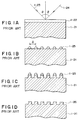
- the period of a diffraction grating used in the optical electronics field is as fine as 0.1 to 1.0 ⁇ m, the conventional photolithography technique cannot be applied to the formation of the photoresist mask. For this reason, a holographic exposure method is normally adopted. This exposure method uses an interference of laser light, and its process will be explained below with reference to Figs. 1A to 1D.
- a photoresist 1-22 is coated on a substrate 1-21.
- Two laser beams 1-23 and 1-24 which are sufficiently parallel light beams are radiated on the photoresist layer from two directions (in Fig. 1A, two directions each forming an angle ⁇ with respect to the perpendicular) to form interference fringes, thereby periodically exposing the photoresist layer.
- the exposed photoresist layer is developed and baked, thereby forming a grating-shaped photoresist mask 1-25, as shown in Fig. 1B.
- etching (wet or dry etching) using the photoresist mask as an etching mask is performed, as shown in Fig. 1C, and thereafter, the etching mask is removed, thereby transferring a periodic structure (diffraction grating) 1-26 to the substrate, as shown in Fig. 1D.
- the He-Cd laser is used.
- the period ⁇ of the diffraction grating becomes as small as about 115 nm from the above equation (in the case utilizing 1st-order diffraction) if the oscillation wave length is 0.8 ⁇ m.
- a sample is dipped in a high-refractive index medium, and interference exposure is performed therein, thereby shortening the period of the diffraction grating by the refractive index of the medium.
- a high-refractive index medium xylene with small light absorption is used.
- a triangular or rectangular prism may be placed on a photoresist film via a refractive index matching oil, and two exposure light beams may be caused to become incident from the two sides of this prism.
- the period of the diffraction grating obtained by a two beams interference exposure method is halved by another treatment.
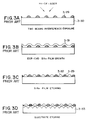
- a plurality of grooves (diffraction grating) 2-27a are formed on a substrate 2-27, and an etching mask material (photoresist) 2-28 is formed on the entire surface of the substrate.
- the etching surface is exposed by exposure and development, as shown in Fig. 2B, and etching is performed, as shown in Fig. 2C, thereby obtaining a diffraction grating having a period half that of the grooves 2-27a, as shown in Fig. 2D.
- a photoresist mask 3-29 is formed on a substrate 3-30 by a two beams interference exposure method, as shown in Fig. 3A, and an SiN x film is grown on the mask by electron cyclotron resonance (ECR)-chemical vapor deposition (CVD), as shown in Fig. 3B.
- ECR electron cyclotron resonance
- CVD chemical vapor deposition
- the etching time is adjusted, thereby forming resist and SiN x etching masks 3-29 and 3-32, as shown in Fig. 3C.
- Etching is performed using these masks, thereby forming a diffraction grating 3-33 having a period half that of the initially formed photoresist mask, as shown in Fig. 3D.
- the manufacture of a wafer multi-layered structure on a manufactured diffraction grating is a very important technique for the sake of improving the semiconductor technique, and the threshold current density of a laser.
- a semiconductor device using a superlattice structure has received a lot of attention since it realizes a semiconductor laser having a lower threshold current and a transistor capable of performing a higher-speed operation as compared to conventional ones.
- a one-dimensional quantum well structure quantum thin film
- a semiconductor laser utilizing this structure is described in the following reference: Tsang, W.T.: "Extremely Low Threshold (AlGa)As Modified Multi-Quantum Well Heterostructure Laser Grown by Molecular Beam Epitaxy" Appl. Phys.
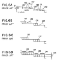
- Figs. 4A, 4B, and 4C are perspective views showing the principles of the one-, two-, and three-dimensional quantum well structures, respectively, and Figs. 5A, 5B, and 5C are graphs each showing the relationship between the density of states and energy shown in Figs. 4A, 4B, and 4C, respectively.
- the density of states of the one-, two-, or three-dimensional structure in a bulk crystal state is defined by a parabola, as indicated by a dotted curve in Fig. 5A
- the curve of the density of states is changed to a staircase shape, sawtooth shape, and pulse train shape respectively in the one-, two-, and three-dimensional quantum well structures. Since it is presumed that a light absorption or light-emission state sequentially changes with such a change in density of states, a semiconductor laser having an extremely low threshold is expected. Furthermore, in the two-dimensional quantum well structure, it is presumed that the electron mobility is increased due to a simplified scattering mechanism, and such a structure is also important in view of electronic devices.
- a substrate having a (100) plane on its surface is inclined at several degrees toward a (011) direction.
- the inclined plane is defined by combining a (100) plane 131 and a (011) plane 133.
- an AlAs molecule 132 flies onto a crystal face (100).
- the AlAs molecule 132 is unstable on the (100) plane, it is re-evaporated or moves on the (100) plane.
- the AlAs molecule 132 is absorbed by this step, and forms a crystal face.
- Quantum confinement in the one-dimensional direction can be achieved with a high precision by thin film formation techniques such as an MBE method.
- certain means for confining a region, corresponding to a well, of an energy band in a barrier region by modulating the energy band in the planar direction in addition to the direction of film thickness is required.
- a GaAs well layer and an AlGaAs barrier layer are grown on a GaAs (001) OFF substrate pre-formed with a three-dimensional pattern using the metal-organic vapor phase epitaxy (MOVPE) method.
- MOVPE metal-organic vapor phase epitaxy
- the light wavefront of an exposure beam is disturbed by scattering or multiple reflections caused by a liquid or its container, or is easily influenced by a vibration of the apparatus and a fluctuation of air, thus impairing the precision of the diffraction grating.
- the second method it is difficult to control the exposure/development conditions after the photoresist film is formed as an etching mask on the entire surface, and a variation occurs in a single plane, thus impairing the precision of the diffraction grating.
- wet etching is used in the second etching process, asymmetry of the diffraction grating shape occurs.
- the etching mask consists of two different materials, i.e., the resist and the SiN x film, these materials have different resistances against an etching gas, resulting in asymmetry of a diffraction grating shape, and low precision of the depth and dimensions.
- the above-mentioned conventional manufacturing method of the two-dimensional quantum well structure utilizes the periodicity of AlAs or GaAs.
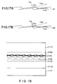
- the AlAs and GaAs layers do not always exhibit constant periodicity, and the widths of the GaAs and AlAs layers often vary, as indicated by 141 and 142 in Fig. 7.
- the quantum wires of the manufactured two-dimensional quantum well structure vary, thus considerably impairing the quantum level and density of states.
- the present invention is to provide a method of manufacturing a laser having two-dimensional quantum wires with high reproducibility without causing the above-mentioned problems.
- the conventional manufacturing method of the quantum wire suffers some problems.
- Prior Art 1 it is difficult to avoid generation of crystal defects caused by micropatterning or the influence of mixing of impurities. Furthermore, it is almost impossible to realize a two-dimensional superlattice in which quantum wires are arranged at a high density by this method.
- Prior Art 2 is superior to that of Prior Art 1 in that there is almost no fear of generation of crystal defects and mixing of impurities since the quantum wire structure is formed in a single growth process.
- the problem of Prior Art 2 is insufficient confinement of carriers due to a large limitation on the dimensions and shape of the wires which can be manufactured. For this reason, it is difficult to manufacture the two-dimensional superlattice.
- Prior Art 3 allows a high-density arrangement of quantum wires in principle.
- this technique is essentially easily influenced by a statistic variation or a fluctuation caused in a surface diffusion process of atoms. For this reason, no high-quality two-dimensional superlattice has been manufactured yet.
- a wavelength-stabilized laser has been enthusiastically studied as a main constituting element of an optical communication device.
- a DFB laser is known.
- the DFB laser will be described below with reference to Figs. 8A to 8D.
- an n-GaAs substrate 340 is used.
- a 0.5- ⁇ m thick Si-doped GaAs layer 341 is stacked on the substrate 340, a 1.5- ⁇ m thick Si-doped AlGaAs lower cladding layer 342 is stacked, and then, a 0.2- ⁇ m thick GRIN layer 343 is stacked.
- An undoped GaAs active layer 344 has a thickness of 6 ⁇ m. After a 0.2- ⁇ m thick upper GRIN layer 345 is stacked on the active layer 344, growth is temporarily stopped (Fig. 8A).
- a grating 346 is formed on the upper GRIN layer 345 (Fig. 8B).
- the grating 346 has a pitch of 240 nm, and is formed by an interference exposure method utilizing He-Cd (Figs. 1A to 1D).
- An upper layer is stacked on the grating 346 formed in this manner. Referring to Fig.
- a 0.3- ⁇ m thick Be-doped AlGaAs light guide layer 347 is formed on the grating 346, a 1.2- ⁇ m thick Be-doped AlGaAs cladding layer 348 is grown on the light guide layer 347, and a 0.5- ⁇ m thick Be-doped GaAs capping layer 349 is formed on the cladding layer 348.
- a ridge 350 is formed in the formed multi-layered films (Fig. 8D). As a result, a current is concentrated on the lower portion of the ridge 350, as indicated by arrows 351. In this manner, a light current confinement structure is formed, and a wavelength-stabilized laser is manufactured.
- this method includes four major processes.
- current confinement and light confinement are attained after growth, resulting in complicated processes.
- a semiconductor device having at least one of a current constriction structure and a quantum wire structure such as a laser having two-dimensional quantum wires, a wavelength-stabilized layer, and the like in a small number of processes with high reproducibility.
- a semiconductor device comprises: a substrate which consists of a semiconductor having one of sphalerite and diamond crystal structures, and has, in at least a portion thereof, a plane orientation inclined at 0.5° to 15° with respect to one of ⁇ 111 ⁇ and ⁇ 110 ⁇ planes indicated by Miller indices; a first semiconductor layer which is formed on the substrate, and has a sawtooth-shaped first periodic structure consisting of one of the ⁇ 111 ⁇ and ⁇ 110 ⁇ planes indicated by the Miller indices and at least one plane indicated by another index; and a second semiconductor layer which is formed on the first semiconductor layer, and has a second periodic structure having a phase shifted from a phase of the first periodic structure.
- a method of manufacturing a semiconductor device comprises the steps of: preparing a substrate which consists of a semiconductor having one of sphalerite and diamond crystal structures, and has, in at least a portion thereof, a plane orientation inclined at 0.5° to 15° with respect to one of ⁇ 111 ⁇ and ⁇ 110 ⁇ planes indicated by Miller indices; forming, on the substrate, a first semiconductor layer which has a sawtooth-shaped first periodic structure consisting of one of the ⁇ 111 ⁇ and ⁇ 110 ⁇ planes indicated by the Miller indices and at least one plane indicated by another index; and forming, on the first semiconductor layer, a second semiconductor layer which has a second periodic structure having a phase shifted from a phase of the first periodic structure.
- a method of manufacturing a semiconductor device comprises the steps of: preparing a substrate which consists of a semiconductor having one of sphalerite and diamond crystal structures, and has, in at least a portion thereof, a plane orientation inclined at 0.5° to 15° with respect to one of ⁇ 111 ⁇ and ⁇ 110 ⁇ planes indicated by Miller indices; forming a diffraction grating on a surface of the substrate; and forming a semiconductor layer on the diffraction grating using one of solid-state source molecular beam epitaxy and gas source molecular beam epitaxy, wherein a direction of a central line of a molecular beam of at least one molecule type forms an angle of 10° to 80° with a normal to a plane orientation of the substrate.
- a ⁇ 111 ⁇ plane includes equivalent planes such as a (111) plane, a (1*1*1*) plane, a (11*1*) plane, and the like
- a ⁇ 110 ⁇ plane includes a (11*0) plane and a (110) plane.
- symbol 1* is a substitution of a symbol of Miller indices, which symbol is expressed by describing "-" above numeral "1". In the following description, this description method is adopted.
- An embodiment of a method of manufacturing a semiconductor device comprises the following steps. The method will be described below with reference to Fig. 9A.
- a diffraction grating 52 having a pitch ⁇ 1 is formed on the surface of a semiconductor substrate 51, which consists of a semiconductor having a sphalerite structure, and has a plane orientation inclined within a range from 0.5° to 15° from a ⁇ 111 ⁇ plane, and a semiconductor crystal is grown on the diffraction grating 52 by a solid-state source molecular beam epitaxy (MBE) method, a gas source molecular beam epitaxy (GSMBE) method using molecular beam sources including some gasified sources, a metal-organic molecular beam epitaxy (MOMBE) method using organic metallic compounds as molecular beam sources, or a chemical beam epitaxy (CBE) method using molecular beam sources, all of which are gasified.
- MBE solid-state source molecular beam epitaxy
- GSMBE gas source mo
- a condition for setting a low growth rate on the ⁇ 111 ⁇ plane is selected, so that a sawtooth pattern 53 consisting of terrace surfaces defined by the ⁇ 111 ⁇ plane and step portions defined by a ⁇ 110 ⁇ plane can be formed.
- a diffraction grating 55 having a pitch ⁇ 1 is formed on the surface of a semiconductor substrate 54 having a plane orientation which is inclined within a range from 0.5° to 15° from a ⁇ 110 ⁇ plane, and a semiconductor crystal is grown on the diffraction grating 55 by the MBE method using solid-state sources, the GSMBE method using molecular beam sources including some gasified sources, the MOMBE method using organic metallic compounds as molecular beam sources, or the CBE method using molecular beam sources, all of which are gasified.
- a condition for setting a low growth rate on the ⁇ 110 ⁇ plane is selected, so that a sawtooth pattern 56 consisting of terrace surfaces defined by the ⁇ 110 ⁇ plane and step portions defined by a ⁇ 113 ⁇ or ⁇ 114 ⁇ plane can be formed.
- the growth progresses mainly in the lateral direction while holding the surface pattern or holding at least the periodic structure of the surface without disappearance of steps.
- a second periodic structure 63 can also be formed, as shown in Fig. 10A.
- the molecular beams can be changed by opening/closing shutters, bubbles, or the like as in the manufacture of a quantum well.
- the period of the periodic structure can be an integer multiple of the pitch of the diffraction grating.
- a second periodic structure having a specific period i.e., a period 1/N that of a pre-formed first periodic structure
- a size 65 of the step portion of the periodic structure formed in this manner is set to be 30 nm or less, a quantum effect can be provided. Furthermore, the size of this portion is determined by the pitch of the diffraction grating, and the inclination angle of the (111) or (110) plane shown in Figs. 9A and 9B.
- the original diffraction grating does not contribute to modulation of an equivalent refractive index.
- the equivalent refractive index of this waveguide has large lower-order components with respect to the pitch of the original diffraction grating, i.e., large components modulated at a short-wavelength pitch as its feature.
- the crystal growth rate of a semiconductor varies depending on its crystal face.
- the growth rate on the (111) plane is lower than that on the (100) plane, and the growth rate on the (110) plane is lower than that on the (111) plane.
- the growth rate on the (110) plane is lower than that on the (111) plane.
- a first periodic structure having a plane orientation inclined within a range from 0.5° to 15° is formed on a semiconductor substrate which consists of a semiconductor having a sphalerite structure, and a ⁇ 111 ⁇ plane orientation.
- a long period having a pitch 10-5 is formed on this substrate surface.
- a surface 10-1 is inclined at 0.5° to 15° from the ⁇ 111 ⁇ or ⁇ 110 ⁇ plane.
- a short-periodic structure is formed on the long-periodic structure.
- the formation process of the short-periodic structure will be described below with reference to Fig. 12.
- an interference exposure method is adopted. This manufacturing method will be described later in the middle of the embodiment.
- Fig. 12 shows a short-periodic structure 11-7 having a pitch of 240 nm formed by the interference exposure method. In this case, the structure 11-7 is formed on a long-periodic structure 11-6.
- a semiconductor crystal is grown on the short-periodic structure by the MBE method using solid-state sources, the GSMBE method using molecular beam sources including some gasified sources, the MOMBE method using organic metallic compounds as molecular beam sources, or the CBE method using molecular beam sources, all of which are gasified.
- Fig. 13 is an enlarged view of a portion around the structure 11-6 in Fig. 12.
- a semiconductor film 12-8 is grown on the short-periodic structure formed on the slope portion of the long-periodic structure.
- a condition for setting a lower growth rate on the ⁇ 111 ⁇ plane than that on the ⁇ 114 ⁇ or ⁇ 113 ⁇ plane as the slope portion is selected, so that a sawtooth pattern 12-11 consisting of terraces defined by the ⁇ 111 ⁇ plane and step portions of the ⁇ 100 ⁇ plane can be formed.
- a semiconductor film 12-9 consisting of a material different from that of the film 12-8 is grown on the sawtooth pattern 12-11 under the same condition.
- a condition setting a low growth rate on the ⁇ 111 ⁇ plane is selected.
- the semiconductor film 12-9 is concentrated on the step portions.
- a semiconductor film 12-10 consisting of a material different from that of the semiconductor film 12-9 is deposited.
- a condition for setting a low growth rate on the ⁇ 111 ⁇ plane is also selected.
- regions having different compositions can be partially formed.
- One important point of this patent is to form planes having different growth rates.
- a surface inclined within a range from 0.5° to 15° may be similarly formed using a substrate having a ⁇ 110 ⁇ plane orientation.
- a plane having a low growth rate and a plane having a high growth rate are formed, the length of one side of the plane having the high growth rate is easily controlled, and the width of the plane having the low growth rate is longer than that of the plane having the high growth rate. If these conditions are satisfied, a semiconductor region can be easily confined even partially.
- a method of growing a semiconductor crystal is selected from the MBE method using solid-state sources, the GSMBE method using molecular beam sources including some gasified sources, the MOMBE method using organic metallic compounds as molecular beam sources, and the CBE method using molecular beam sources, all of which are gasified.
- Fig. 14 is a partially enlarged view of Fig. 10A.
- a diffraction grating 13-21 is formed by the interference exposure method.
- a pitch ⁇ 1 of the grating is 240 nm.
- the width B (13-24 of the (100) plane forming the step is 26 nm.
- a crystal is grown on this structure by epitaxial growth.
- the growth rate on the (111) plane is faster by three times than the growth rate on the (100) plane.
- a quantum well 14-31 is formed on the step.
- a 20-nm thick film 14-32 is stacked on the (100) plane.
- a GaAs film 14-33 having a thickness of 6 nm about 1/3 that of the film 14-32 is stacked on the (111) plane.
- Fig. 15 shows a state wherein the films 14-32 and 14-33 are repetitively stacked. These films can be easily stacked by changing source materials.
- a diffraction grating is formed on a semiconductor substrate inclined at 0.5° to 15° from the ⁇ 111 ⁇ or ⁇ 110 ⁇ plane, and a semiconductor crystal is grown thereon by the MBE or GSMBE method.
- the incident direction of molecular beams is not particularly limited.
- the GSMBE method is also called a chemical beam epitaxy (CBE) method or a metal-organic molecular beam epitaxy (MOMBE) method, these methods imply the same scheme.
- the orientation of a low index face of a crystal has a minimal growth rate.
- the ⁇ 111 ⁇ plane (or ⁇ 110 ⁇ plane) has a very low growth rate, a sawtooth pattern consisting of terraces of the ⁇ 111 ⁇ plane (or ⁇ 110 ⁇ plane) and steps having a plane orientation different from the ⁇ 111 ⁇ plane (or ⁇ 110 ⁇ plane) is formed in the crystal growth.
- S P ⁇ sin(a)
- T P ⁇ cos(a)
- the growth rate on the terrace plane is extremely low, and hence, almost no molecules are absorbed, most of molecules incident on the surface reach the step portion and are absorbed by a crystal, or desorbed into a vacuum phase.
- the ratio of molecules crystallized on the terrace plane is very small.
- the sawtooth pattern is held on the surface without disappearance of steps, and growth in the lateral direction progresses almost steadily.
- Vs be the lateral growth rate of the step portion measured in the horizontal direction with respect to the terrace plane
- Vt be the growth rate of the terrace portion in the vertical direction with respect to the terrace plane
- a quantum wire having very small dimensions can be manufactured with high precision.
- a two-dimensional superlattice in which quantum wires are arranged at a high density can be formed.
- the proper period is expressed by, e.g., T/(N + 1/2) (where N is an integer).
- Fig. 16 shows a multi-layered structure of a wafer for a GaAs/AlGaAs-based DFB laser according to the first embodiment of the present invention, which has a 1st-order diffraction grating having a pitch of 125 nm.
- An Si-doped GaAs substrate 15-11 is a so-called inclined substrate whose substrate surface is inclined at 5° from a (111) A plane in a (100) plane direction.
- a 0.5- ⁇ m thick Si-doped GaAs buffer layer 15-12 is formed on the substrate 15-11, and a 1.5- ⁇ m thick Si-doped Al 0.5 Ga 0.5 As cladding layer 15-13 is formed on the layer 15-12.
- a 200-nm thick Si-doped Al y Ga 1-y As layer 15-14 serves as a light confinement region.
- the Al content y of the layer 15-14 gradually changes from 0.5, and decreases to 0.3 near an active layer 15-15.
- a multi-quantum well structure of the active layer consists of five quantum wells constituted by repetitively forming a 10-nm thick undoped Al 0.3 Ga 0.7 As barrier layer and a 6-nm thick undoped GaAs well layer.
- a 0.3- ⁇ m thick Be-doped Al 0.3 Ga 0.7 As layer as an upper light guide layer 15-16 is formed on the active layer 15-15.
- a resist pattern having a pitch of 250 nm is formed on the surface of the layer 15-16 using a laser interference exposure method, and a 2nd-order diffraction grating 15-17 is formed by dry etching.
- the direction of each groove of the grating is perpendicular to a plane defined by the (110) direction, i.e., the normal to the original substrate and the normal to the (111) A plane.
- an Al 0.3 Ga 0.7 As layer 15-18 having the same composition as that of the upper light guide layer, and having an average film thickness of 0.2 ⁇ m is grown on the diffraction grating, thus forming periodic steps on the surface.
- Each step is defined by a terrace plane of the (111) A plane having a width of about 225 nm, and a step plane of a (001) plane having a width of about 38 nm.
- the period of repetition coincides with the period of 250 nm of the diffraction grating, and the level difference between adjacent steps is about 20 nm.
- V00 the GaAs growth rate on a flat substrate
- V03 the Al 0.3 Ga 0.7 As growth rate
- Vg00 the propagation rate of the growth surface on the diffraction grating with respect to GaAs
- Vg03 the propagation rate with respect to Al 0.3 Ga 0.7 As
- ⁇ g00 be the angle defined by the growth direction and the normal to the substrate with respect to GaAs
- ⁇ g03 be the angle with respect to Al 0.3 Ga 0.7 As (see Figs. 17A and 17B)
- V00 11 nm/min
- V03 15.7 nm/min
- Vg00 V00/cos ⁇ g00
- Vg03 V03/cos ⁇ g03
- V103 V03/tan ⁇ g03 , thus revealing the propagation rates of the growth surface in the horizontal direction.
- V100 29.5 nm/min
- V103 42.1 nm/min.
- a periodic structure 15-19 consisting of a Be-doped GaAs layer and a Be-doped Al 0.3 Ga 0.7 As layer is formed by opening/closing a shutter. More specifically, when a GaAs layer is grown for 1 minute and 41 seconds, subsequently, an AlGaAs layer is grown for 1 minute and 47 seconds, a GaAs layer is grown again for 1 minute and 41 seconds, and subsequently, an AlGaAs layer is grown for 1 minute and 47 seconds, the periodic structure of the growth surface progresses by 250 nm in the horizontal direction. During this interval, the growth surface progresses by about 88 nm in the vertical direction.
- the repetitive period of the periodic structure in a direction parallel to the substrate surface is 125 nm, and a refractive index modulation structure having a period 1/2 the pitch of the formed diffraction grating can be manufactured.
- the growth condition is changed, so that the growth rate on the (111) plane is high as well.
- a 0.2- ⁇ m thick Be-doped Al 0.3 Ga 0.7 As layer 15-191 is formed to flatten the growth surface, and a 1.5- ⁇ m thick Be-doped Al 0.5 Ga 0.5 As upper cladding layer 15-192 and a 0.3- ⁇ m thick Be-doped GaAs capping layer 15-193 are formed on the layer 15-191, thus forming an LD structure.
- the equivalent refractive index is modulated by thick GaAs portions arranged in the upper guide layer at 125-nm intervals.
- Fig. 18 shows a waveguide with a diffraction grating having a semi-periodic structure according to the second embodiment of the present invention.
- An Si-doped GaAs substrate 17-71 is an inclined substrate whose substrate surface is inclined at 5° from a (111) A plane in a (100) plane direction.
- a 1.0- ⁇ m thick Si-doped Al 0.5 Ga 0.5 As cladding layer 17-72 is formed on the substrate 17-71.
- a waveguide layer 17-73 consists of a 200-nm thick undoped Al 0.1 Ga 0.9 As layer.
- a 0.3- ⁇ m thick Be-doped Al 0.3 Ga 0.7 As layer 17-74 as an upper light guide layer is formed on the layer 17-73.
- a resist pattern having a pitch of 250 nm is formed on the surface of the layer 17-74 using a laser interference exposure method, and a 2nd-order diffraction grating is formed by dry etching. After the resist residue and oxides on the surface are removed in an MBE chamber, an Al 0.3 Ga 0.7 As layer is grown on the diffraction grating by the GSMBE method.
- a periodic structure 17-75 consisting of a Be-doped Al 0.1 Ga 0.9 As layer and a Be-doped Al 0.3 Ga 0.7 As layer are formed by controlling the supply amounts of source materials using mass-flow controllers. Even when a new facet is formed since the growth surface cannot keep a similar shape, a refractive index modulation structure having a period 1/2 the pitch of the diffraction grating can be manufactured, as shown in Fig. 10B.
- the growth rate on the (111) plane is set to be large by changing the growth condition, and a 0.2- ⁇ m thick Be-doped Al 0.3 Ga 0.7 As layer 17-76 is formed to flatten the growth surface.
- a 1.5- ⁇ m thick Be-doped Al 0.5 Ga 0.5 As upper cladding layer 17-77 and a 0.3- ⁇ m Be-doped GaAs capping layer are formed on the layer 17-76.
- Fig. 19 shows a two-dimensional quantum well manufactured using the method of the present invention.
- a substrate 18-41 is an Si-doped GaAs substrate. This substrate has a structure inclined at 2° from the (111) plane in the (110) plane direction.
- the growth film is taken out from a growth apparatus, and a diffraction grating is formed on the layer 18-43 by interference exposure.
- the growth film with the diffraction grating formed in this manner is placed in a growth chamber again.
- a diffraction grating 18-44 shown in Fig. 19 is formed.
- An undoped GaAs well 18-46 constituting an active layer is grown on the layer 18-45 to have a thickness of about 10 nm on the (100) plane. At this time, the film thickness of the GaAs layer on the (111) plane is 3 nm or less.
- a 0.5- ⁇ m thick Be-doped GaAs capping layer is grown on the cladding layer, thus completing a laser.
- the threshold current density of the manufactured two-dimensional quantum well can be improved by about 30% as compared to that of a conventional one-dimensional quantum well.
- Fig. 20 shows the fourth embodiment of the present invention.
- the characteristic feature of this embodiment is to arrange a carrier block layer 19-65.
- an Si-doped GaAs substrate 19-61 has a (111) plane, and is inclined at 5° in a (110) plane direction.
- the growth film is placed again in a growth chamber, and re-growth is performed.
- the MOCVD method is used in both the primary growth and re-growth processes. In a gas-based growth method, a large selectivity ratio on the (111) and (100) planes can be selected as compared to solid-state source growth as in the MBE method, and a more stable quantum wire can be formed.
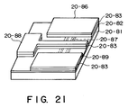
- Fig. 21 is a perspective view showing a field effect transistor using a quantum wire manufactured according to the method of the present invention.
- a substrate 20-81 comprises an undoped GaAs substrate.
- the (110) plane substrate is inclined at 5° toward a ⁇ 111 ⁇ direction.
- a diffraction grating is formed, and is subjected to re-growth to manufacture a quantum wire.
- a facet formed with the quantum wire is defined by the (110) and (100) planes.
- a selectivity ratio of 1 : 10 or higher can be selected.
- Contact layers 20-83 correspond to the source, drain, and gate.
- the field effect transistor includes electrodes 20-86, 20-87, and 20-88.
- Fig. 22 shows the sixth embodiment of the present invention.
- a diffraction grating 21-2 is formed, by utilizing the laser inference exposure method, on the surface of a GaAs substrate 21-1, which is inclined at 5° from the (111) plane to have a [110] direction as the rotational axis.
- This diffraction grating has a stripe direction [110], a period of 0.24 ⁇ m, and an amplitude of 0.1 ⁇ m.
- GaAs and AlGaAs crystals are grown on the diffraction grating by the GSMBE method using trimethyl gallium (TMGa), triethyl aluminum (TEAl), and AsH3 as source gases.
- TMGa trimethyl gallium
- TEAl triethyl aluminum
- AsH3 AsH3
- An arrow 21-3 indicates the incidence direction of TMGa and TEAl molecular beams, and is inclined at 50° from the normal direction to the substrate.
- An arrow 21-4 indicates the incidence direction of an AsH3 molecular beam, and is inclined at 10° from the normal direction to the substrate to the side opposite to the TMGa molecular beam.
- An AlGaAs layer 21-5 is grown on the diffraction grating, and a sawtooth pattern defined by terraces 21-6 and steps 21-7 is formed on the surface of the layer 21-5.
- the plane orientation of the terrace is (111), and the height of the step is about 21 nm.
- the growth rate Vt in a direction perpendicular to the terrace plane is almost negligibly small, and a steady state wherein the growth progresses upon movement of the step in the lateral direction is achieved.
- Fig. 23 shows the seventh embodiment of the present invention.
- a diffraction grating 22-14 is formed, using the light interference exposure method, on the surface of a GaAs substrate 22-13, which is inclined at 5° from a (111) plane to have a [110] direction as the rotational axis.
- This diffraction grating has a stripe direction [110], a period of 0.1 ⁇ m, and an amplitude of 0.05 ⁇ m.
- GaAs and AlGaAs crystals are grown on the diffraction grating by the MBE method using Ga, Al, and As as solid-state sources.
- An arrow 22-15 indicates the incident direction of Ga and Al molecular beams, and is inclined at 50° from the normal direction to the substrate.
- an arrow 22-16 indicates the incident direction of an As molecular beam, and is inclined at 20° from the normal direction to the substrate to the side opposite to the Ga molecular beam.
- An AlGaAs layer 22-17 is grown on the diffraction grating, and a sawtooth pattern defined by terraces 22-18 and steps 22-19 is formed on the surface of the layer 22-17.
- the plane orientation of the terrace is (111), and the height of the step is 21 nm.
- a growth rate Vt in a direction perpendicular to the terrace plane is about 1/10 of a growth rate Vs, in the lateral direction, of the step, and a steady state wherein the growth progresses upon movement of the step in the lateral direction is achieved.
- a periodic structure having a period 1/N of that of a periodic structure formed on the inclined substrate can be added. Since the period of the diffraction grating becomes a fraction of the period of the diffraction grating formed by the interference exposure method, the period of the diffraction grating to be formed can be easily controlled by the interference exposure method. Furthermore, a quantum wire can be obtained with high reproducibility.
- a quantum wire having a sufficient confinement effect for carriers in a semiconductor, and a two-dimensional superlattice in which such quantum wires are arranged at a high density can be relatively easily manufactured with high reproducibility.
- a III-V film having an amphoteric impurity is epitaxially grown on a semiconductor substrate having a sphalerite structure (zinc blende structure) such as GaAs, and having a periodic three-dimensional pattern, which commonly has a surface on which a Ga plane is easily formed in at least a portion thereof with a region having a surface orientation inclined within a range from 0° to 20° with respect to a ⁇ 100 ⁇ plane, thereby obtaining a semiconductor laser having a current constriction layer without any processes after growth.
- the ⁇ 100 ⁇ plane includes equivalent planes such as a (100) plane, a (010) plane, a (001) plane, and the like.
- Si serves as an amphoteric impurity for a III-V compound.
- Si When Si is replaced with a Ga site, it changes the polarity to n type; when Si is replaced with an As site, it changes the polarity to p type.
- the growth surface In order to allow easy replacement with Ga, the growth surface must be covered with As, and an As dangling bond must be exposed on the surface. This situation can be realized by a plane called a B plane, and can also be obtained by a (511) A plane, a (611) A plane, and the like.
- a Ga plane In order to replace the As site with Si, a Ga plane must be stably formed on the surface.
- a plane for realizing this condition includes a (311) A plane, a (211) A plane, a (111) A plane, and the like.
- a periodic three-dimensional pattern is formed on a semiconductor substrate which has a zinc blende structure such as GaAs, and has, in at least a portion thereof, a region having a surface orientation inclined within a range from 0° to 15° with respect to a ⁇ 111 ⁇ or ⁇ 110 ⁇ plane, and a III-V film having an amphoteric impurity is epitaxially grown on the three-dimensional pattern and another flat surface, thereby forming a current constriction layer.
- a zinc blende structure such as GaAs
- the ⁇ 111 ⁇ plane includes equivalent planes such as a (-111) plane, a (1-11) plane, a (-1-11) plane, and the like, and the ⁇ 110 ⁇ plane includes a (-110) plane, a (1-10) plane, and the like.
- the crystal growth rate of a semiconductor varies depending on the crystal face involved. For example, a (-111) plane has a lower growth rate than that of a (100) plane, and a (-110) plane has a lower growth rate than that of a (111) plane (for further details, refer to an article "Journal of Applied Physics Vol. 64, 3522 (1988)). By utilizing this fact, a quantum wire can be easily manufactured.
- a grating having a pitch ⁇ 1 is formed on a substrate 202, which consists of a semiconductor having a zinc blende structure, and has a surface orientation inclined within a range from 0° to 15° from the ⁇ 111 ⁇ or ⁇ 110 ⁇ plane.
- An interference exposure method is utilizes as a manufacturing method. The manufacturing method will be described later in the middle of the embodiment. Referring to Fig. 24, a periodic structure 207 having a pitch of 240 nm is formed by the interference exposure method.
- semiconductor crystals are grown on the periodic structure 207 by an MBE method using solid-state sources, a GSMBE method using molecular beam sources including some gasified sources, an MOMBE method using organic metallic compounds as molecular beam sources, or a CBE method using molecular beam sources all of which are gasified.
- a semiconductor film 208 is grown on the periodic structure 207.
- a condition for setting a lower growth speed on a flat plane e.g., the ⁇ 111 ⁇ plane
- a plane of a slope portion e.g., near the ⁇ 100 ⁇ plane, for example, a ⁇ 114 ⁇ plane, a ⁇ 113 ⁇ plane, or the like
- a sawtooth pattern 211 consisting of terrace portions 212 each defined by the ⁇ 111 ⁇ plane and step portions 213 each defined by the ⁇ 100 ⁇ plane can be formed.
- a semiconductor film 209 consisting of a material different from that of the semiconductor film 208 is grown on the sawtooth pattern under the same condition. At this time, a condition for setting a lower growth rate on the ⁇ 111 ⁇ plane 212 is selected. As a result, the semiconductor film 209 is concentrated on the step portions 213, as shown in Fig. 24. Similarly, a semiconductor film 210 different from the semiconductor film 209 is deposited. At this time, a condition for setting a lower growth rate on the ⁇ 111 ⁇ plane is selected as well. Upon repetition of these processes, regions 209 and 210 having different compositions can be locally formed. One important point of the present invention is to form planes of different growth rates.
- a semiconductor crystal growth method includes the MBE method using solid-state sources, the GSMBE method using molecular beam sources including some gasified sources, the MOMBE method using organic metallic compounds as molecular beam sources, and the CBE method using molecular beam sources all of which are gasified.
- a semiconductor film having a specific period can be formed on the substrate 202 having an inclined region.
- the size of the step portion 213 of the periodic structure formed in this manner is set to be 30 nm or less, a quantum effect can be provided.
- a size 224 of the portion 213 is determined by the pitch ⁇ 1 of the grating 207 and the inclination angle of the (111) plane or (110) plane 212.
- the pitch ⁇ 1 of the grating 207 formed by the interference exposure method is 240 nm.
- ⁇ ' is an angle 223 defined between the ⁇ 111 ⁇ plane 212 and the (100) plane 213 forming the step portion, and is 54.7°.
- the width 224 of the (100) plane 213 forming the step portion is 26 nm.
- a crystal is grown on the grating by epitaxial growth.
- the ratio of the growth rate on the (111) plane 212 to that of the (100) plane 213 is about 1 : 3, and the growth rate on the (100) plane 213 is higher by about three times than that on the (111) plane 212.
- quantum wires are formed at positions corresponding to the step portions 213.
- a multi-layered structure can be easily realized, as shown in Fig. 24.
- Si serves as an amphoteric impurity for a III-V compound.
- Si When Si is replaced with a Ga site, it changes the polarity to n type; when Si is replaced with an As site, it changes the polarity to p type.
- a p-type GaAs layer can be formed.
- an Si-doped GaAs layer is grown on a ⁇ 100 ⁇ plane, an n-type GaAs layer can be formed.
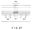
- Fig. 28 shows a two-dimensional quantum well (quantum wire) laser comprising a current constriction layer (the resonance direction corresponds to the vertical direction of Fig. 28).
- a substrate 251 is an Si-doped GaAs substrate.
- the substrate 251 has a plane inclined at 5° from the (111) plane.
- the exposure is performed in a procedure described previously with reference to Figs. 1A to 1D.
- a three-dimensional pattern having a large period is formed by normal exposure.
- the interference exposure is performed.
- a photoresist 1-22 is coated on a growth film 1-21, and two laser beams 1-23 and 1-24, which are collimated to sufficiently parallel beams, are radiated onto the photoresist from the two directions, thereby forming interference fringes.
- the photoresist 1-22 is periodically exposed, and is developed, thereby forming a grating-shaped photoresist mask 1-25, as shown in Fig. 1B.
- Etching is performed using the photoresist mask 1-25 as an etching mask, as shown in Fig. 1C, and thereafter, the etching mask 1-25 is removed, thereby transferring a periodic structure 1-26 to the growth film 1-21, as shown in Fig. 1D.
- the He-Cd laser is used, and the desired grating pitch ⁇ is determined by changing ⁇ . In this manner, the diffraction grating is formed to have a pitch of 240 nm.
- the growth film 1-21 with the diffraction grating formed in this manner is placed again in a growth chamber.
- This diffraction grating is a locally formed diffraction grating or a grating 260, as shown in Fig. 28.
- steps defined by the (111) and (100) planes are formed, and the width of the (100) plane as an inclined plane is about 10 nm.
- n-type regions are formed on the inclined surface portions of the diffraction grating 260, and p-type regions are formed on upper portions of the diffraction grating 260.
- An Sn-doped GaAs layer 262 is grown on the Si-doped AlGaAs layer 261 as a current constriction layer. This layer becomes an n-type layer. As a result, an npn junction is formed in a direction parallel to the substrate surface.
- the layer 262 grown on the (100) plane has a thickness of about 10 nm. At this time, the film thickness of the GaAs layer 262 on the (111) plane is 3 nm or less.
- a current 268 flows a portion where the diffraction grating 260 is formed, the Si-doped AlGaAs layer 261 on which no diffraction grating 260 is formed has p conductivity type, and no current flows therethrough. The manufactured laser exhibits a good current constriction effect.
- Fig. 29 shows the ninth embodiment in which the present invention is applied to a multi-quantum well laser (the resonance direction corresponds to the vertical direction of Fig. 29).
- the characteristic feature of this embodiment is to provide a carrier block layer 275.
- a current flows only through a portion corresponding to each inclined surface portion of a diffraction grating 286, thus constricting the current.
- the structure of this embodiment will be described below with reference to Fig. 29.
- a substrate 271 is an Si-doped GaAs substrate.
- the substrate 271 has a plane inclined at 10° from the (111) plane.
- a three-dimensional pattern i.e.
- convex and concave structure having a large period of 200 mm is formed by a normal exposure method, and a diffraction grating 286 having a pitch of 250 nm is formed by a grating formation method based on the interference exposure method.
- the wafer is placed again in a growth apparatus, and re-growth is performed.
- a current channel is formed on inclined surface portions, as has been described above.
- an active region is stacked on the layer 275.
- an npn junction is formed, thus blocking a current.
- the above-mentioned processes are repeated to form a layer 278 (barrier layer), a layer 279 (well layer), a layer 280 (barrier layer), and a layer 281 (well layer).
- a layer 282 is a barrier layer, it is formed to be relatively thick, and the selectivity ratio of the growth rates on the (111) and (100) planes is decreased. As a method of decreasing the selectivity ratio, the substrate temperature is decreased.
- a 100-nm thick light guide layer 283 is stacked.
- the layer 283 comprises a Be-doped AlGaAs layer, and the Al composition is decreased from 0.3 to 0.5.
- a 1.5-nm thick Be-doped AlGaAs layer 284 as a cladding layer is stacked on the layer 283.
- a 0.5-nm thick Be-doped GaAs layer 285 is tacked, thus completing a laser structure.
- the MOCVD method is used in both the primary growth and re-growth processes.
- a large selectivity ratio on the (111) and (100) planes can be selected as compared to solid-state source growth as in the MBE method, and a more stable quantum wire can be formed.
- a current is confined in the diffraction grating portion 286.
- the current constriction layer structure is simultaneously formed.
- another conventional current constriction structure may be manufactured, and a quantum wire structure alone may be formed.
- a grating 207 is formed on a substrate 202. Assume that this layer is an n-type GaAs layer. Note that a plane forming an angle of 20° or less with a ⁇ 100 ⁇ plane 232 is exposed on inclined surface portions of the grating 207.
- an Si-doped GaAs or AlGaAs layer is grown on the grating, an n-type layer 234 is grown on the grating inclined surface portions, and a p-type layer is formed on portions near the vertices of the grating 207.
- both p- and n-type regions are locally formed.
- the n-type layer 234 having the same polarity as that of the underlying layer 207 is formed on the inclined surface portions of the grating.
- a layer 238 (Si-doped AlGaAs) stacked on the layer 234 also has discrete n-type regions 234 separated in the lateral direction.
- a layer 239 is an Sn-doped AlGaAs layer, which allows formation of a uniform n-type region. As a result, a current flows from the grating region 207 toward the upper portion through the regions 234, as indicated by bold slant arrows 236.
- a film grown on a portion corresponding to a ⁇ 111 ⁇ A plane 233 has p conductivity type since Si enters an As site. Therefore, a p-n junction is formed at an interface between the grating (n-type) 207 and the layer 238, and an n-p junction is formed at an interface between the layer (n-type) 239 and the layer 238. As a result, a current 237 is blocked, and cannot reach the layer 239.
- the layer 239 is an n-type GaAs or AlGaAs region, as described above. A current is also blocked by a region corresponding to a ⁇ 111 ⁇ A plane 231, i.e., a flat region shown in Fig.
- a current is constricted by a combination of a change in p-n junction of the Si-doped AlGaAs film, and the Sn-doped (n-type) or Be-doped (p-type) layer.
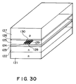
- a semiconductor laser using a current constriction effect formed by the above-mentioned processes will be described below with reference to Fig. 30.
- a semiconductor laser shown in Fig. 30 comprises an n-type GaAs substrate 121 having a (100) crystal face, an Si-doped AlGaAs layer 122 (about 1.5 ⁇ m thick) as a cladding layer, an undoped GaAs layer 123 as an active layer, and a Be-doped AlGaAs layer 124 (p-type, 0.4 ⁇ m thick) as a light confinement layer.
- a grating 128 is formed on the layer 124 to have a pitch of 500 nm.
- the grating 128 is formed by ammonium-based wet etching.
- Each inclined surface portion formed in this case is defined by a (211) plane.
- the inclined surface portion has a depth of about 150 nm.
- a 0.2- ⁇ m thick Si-doped AlGaAs layer 125 is formed on the layer 124 formed in this manner.
- a 0.1- ⁇ m thick Be-doped GaAs layer 126 (p-type) as an interference layer, and a 1.8- ⁇ m thick Be-doped AlGaAs or GaAs layer 127 is formed on the layer 126.
- a portion corresponding to each inclined surface portion 129 of the grating 128 has p conductivity type, as indicated by a region 130.
- a flat surface portion has n conductivity type.
- the 1.8- ⁇ m thick Be-doped AlGaAs or GaAs layer 127 is formed on the film in which a p-n junction is formed in the lateral direction.
- a current flows toward the upper portion through a region corresponding to the grating 128.
- a pnp junction is formed by a combination of the layers 124, 125, and 126, and blocks a current.
- the wafer need not be processed after the growth, and the number of steps can be decreased.
- the ratio of As to Ga or Al of the III group is preferably decreased as much as possible.
- the ratio of V/III is set to be 2 or less.
- the grating is formed parallel to a resonator to provide a current constriction effect, thus realizing light confinement in the lateral direction as well.
- a semiconductor laser structure wherein a grating is formed in a direction perpendicular to a resonator will be described below.
- a substrate 151 is an n-type GaAs substrate.
- the substrate 151 has a (100) crystal face, and a 1.8- ⁇ m thick Si-doped AlGaAs layer 152 as a cladding layer is stacked on the substrate.
- An undoped GaAs layer 153 as an active layer, and a Be-doped AlGaAs layer (p-type, 0.4 ⁇ m thick) 154 as a light confinement layer are sequentially formed on the layer 152.
- a grating 156 having a pitch of 240 nm is formed on the layer 154. The diffraction grating is formed since the laser of this embodiment is used as a wavelength-stabilized laser, and the laser of this embodiment serves as a DFB laser.
- a 0.1- ⁇ m thick Si-doped AlGaAs layer 155 is formed on the grating. Furthermore, a 0.1- ⁇ m thick Be-doped GaAs layer 158 (p-type) as an interference layer is stacked on the layer 155, and a 1.8- ⁇ m thick Be-doped AlGaAs or GaAs layer 160 is formed thereon.
- a portion of the Si-doped AlGaAs layer 155 corresponding to each inclined surface portion 157 of the grating 156 has p conductivity type, as indicated by a region 159. Note that a flat surface portion has n conductivity type.
- the 1.8- ⁇ m thick Be-doped AlGaAs or GaAs layer 160 is formed on a film in which a p-n junction is formed in the lateral direction.
- a current flows toward an upper portion through a region corresponding to each inclined surface portion 157.
- a pnp junction is formed by a combination of the layers 154, 155, and 158, and blocks a current.
- the wafer need not be processed after the growth, and the number of steps can be decreased.
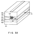
- Fig. 32 shows the 12th embodiment of the present invention.
- the characteristic feature of this embodiment is that a trapezoidal active region is formed to change a refractive index n in the lateral direction.
- an n-type GaAs substrate 161 has a (100) plane.
- a 1.8- ⁇ m thick Si-doped GaAs or AlGaAs layer 162 is grown on the substrate, and a 0.08- ⁇ m thick undoped GaAs layer 163 as an active layer is grown thereon.
- a 0.4- ⁇ m thick Be-doped AlGaAs layer 167 (p-type) is formed. After the layer 167 is formed, a ridge is formed on a portion corresponding to a current constriction region.
- a grating 166 is formed on the ridge to have a pitch of 220 nm.
- Each of formed inclined surface portions 168 is defined by a (311) A plane.
- a 1.0- ⁇ m thick Si-doped AlGaAs layer 164 is grown on the grating.
- a p-type region is formed in a region of the layer 164 corresponding to each inclined surface portion 168 of the grating 166. In contrast to this, an n-type region is formed in a flat region. Therefore, a ridge portion indicated by a region 170 has p conductivity type.
- a 0.4- ⁇ m thick Be-doped AlGaAs layer 165 (p-type) is formed on the layer 164, and a 0.5- ⁇ m thick Be-doped GaAs layer 169 is formed thereon. In this manner, light can be confined in the active region.
- a mechanism for forming a pnp junction by a combination of the layers 167, 164, and 165, and blocking a current is the same as that in the above embodiment.
- a plane orientation 171 indicates a [011] or [0-1-1] orientation.
- the wafer need not be processed after the growth.
- Fig. 33 shows the 13th embodiment of the present invention. In this embodiment, the light confinement effect in the lateral direction is further enhanced.
- an n-type GaAs substrate 172 has a (100) plane orientation.
- a 0.8- ⁇ m thick Si-doped GaAs layer 173 is stacked on the substrate, and thereafter, a ridge 174 is formed.
- the ridge 174 has a width of about 3 ⁇ m at its upper portion, and has a height of 1 ⁇ m.
- a grating 176 is formed on the ridge 174. The pitch of the grating 176 is 260 nm.
- a plane orientation 179 indicates a [01-1] orientation.
- a plane orientation 178 indicates a [011] orientation, and a plane orientation 175 indicates a [100] orientation.
- a portion corresponding to each inclined surface portion of the grating 176 has p conductivity type, and a portion corresponding to each inclined surface portion indicated by a region 177 has n conductivity type.
- This phenomenon occurs depending on which of Ga and As is stably present on the surface. Since Ga is stably present on each inclined surface portion of the grating 176, Si enters an As site, and a p-type region is grown. Contrary to this, since As is stable on the region 177, Si enters a Ga site, and an n-type region is formed. By utilizing this phenomenon, a current and light can be confined by a single growth process.
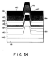
- Fig. 34 shows a structure utilizing the above-mentioned arrangement.
- a p-type GaAs layer 181 has a (100) plane orientation.
- a 0.8- ⁇ m thick Be-doped GaAs layer 182 is grown on the layer 181, and thereafter, a ridge 185 is formed by etching.
- the ridge 185 extends in a [011] direction, and an As-stabilized plane such as a (111) B plane is exposed on the inclined surface portion of the ridge.
- the ridge 185 has a height of 1 ⁇ m, and a width of 4 ⁇ m at its upper portion.
- a 1.5- ⁇ m thick Be-doped AlGaAs layer 183 is grown on the ridge.
- a grating having a pitch of 200 nm is formed on the upper portion of the ridge of the Be-doped AlGaAs layer 183.
- a 0.1- ⁇ m thick Si-doped AlGaAs layer 184 is formed on the grating, and a 0.1- ⁇ m thick Be-doped AlGaAs layer 188 is formed thereon.
- a 0.2- ⁇ m thick Si-doped AlGaAs layer 189 is formed.
- the layers near an upper portion 187 of the ridge have p conductivity type even when Si is doped, since the A plane is formed on the inclined surface portion of the grating. Therefore, in this portion, all the layers 184, 188, and 189 have p conductivity type, and a current can easily flow. In contrast to this, in a flat portion, the layers 184, 188, and 189 form an npn junction, and block a current.
- an undoped GaAs layer (0.1 ⁇ m thick) 190 as an active layer is formed on the layer 189.
- the layer 190 has an active region 193, and a current is efficiently concentrated on the active region 193. Furthermore, light can also be confined by changing the layer pattern.
- An Sn-doped AlGaAs layer (n-type, 1.5 ⁇ m thick) 191 as an upper cladding layer is formed on the layer 190, and an Sn-doped GaAs layer (n-type, 0.5 ⁇ m thick) 192 as a capping layer is formed thereon.
- Fig. 35 shows a laser having a GRIN region.
- an n-type GaAs substrate 401 has a (100) plane.
- a 0.5- ⁇ m thick Si-doped GaAs layer 402, a 1.5- ⁇ m thick Si-doped AlGaAs layer 403, and a 0.2- ⁇ m thick GRIN region 404 whose composition is gradually changed are sequentially stacked on the substrate 401.
- a quantum well layer (6 nm thick) 405 is formed on the GRIN region 404, and an upper GRIN region 406 is formed on the layer 405. Note that undoped layers are formed in this case, but doped layers may be formed.
- a p-type AlGaAs layer 407 is formed on the region 406.
- a grating 408 is formed on the layer 407, and an Si-doped AlGaAs layer 409 is stacked thereon.
- a plane corresponding to each inclined surface portion has p conductivity type.
- a 1.5- ⁇ m thick Be-doped AlGaAs layer 411 (p-type), and a 0.5- ⁇ m thick Be-doped GaAs layer 412 are formed.
- a mechanism for forming a pnp junction by a combination of the layers 407, 409, and 411, and blocking a current is the same as that in the above embodiment.
- a current confinement structure can be applied to a laser having a quantum well structure.
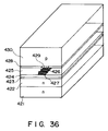
- Fig. 36 shows an embodiment wherein the present invention is applied to an InGaAs/InP-based DFB laser.
- a substrate 421 is an n-type InP substrate.
- a 2- ⁇ m thick Si-doped n-type InP layer 422 is grown on the substrate.
- an undoped Ga 0.47 In 0.53 As layer 423 as an active layer is grown, and a 0.1- ⁇ m thick Be-doped p-type InP layer 424 is grown.
- a 1st-order grating 426 having a pitch of 240 nm is formed.
- An inclined surface 427 is formed as a plane inclined at 20° or more from a (100) plane.
- etching is performed using Br methanol as an etchant.
- a film grown on the (111) A plane 427 has p conductivity type
- a film grown on the (100) plane has n conductivity type.
- a 0.2- ⁇ m thick Be-doped p-type InP layer 428 is grown, and in a flat portion defined by the (100) plane, a pnp junction is formed by the layers 424, 425, and 428, thus blocking a current.
- the layer 425 has p conductivity type, as indicated by a region 429.
- a Be-doped InP layer 430 has p conductivity type.
- a film grown on a portion where the grating is formed has p conductivity type.
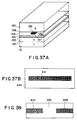
- Fig. 37A shows an embodiment wherein a current constriction portion is modified.
- the film structure is the same as that in Fig. 31. More specifically, an n-type GaAs substrate 151 has a crystal face defined by the (100) plane, and a 1.8- ⁇ m thick Si-doped AlGaAs layer 152 as a cladding layer is stacked on the substrate. An undoped GaAs layer 153 as an active layer, and a Be-doped AlGaAs layer (0.4 ⁇ m thick) 154 as a light confinement layer are sequentially formed on the layer 152.
- a grating 156 is formed on the layer 154 to have a pitch of 240 nm. In this case, the grating has a depth of 150 nm.
- the diffraction grating is formed since the laser of this embodiment is used as a wavelength-stabilized laser as in Fig. 31.
- a 0.1- ⁇ m thick Si-doped AlGaAs layer 155 is formed on the structure formed as described above.
- a 0.1- ⁇ m thick Be-doped GaAs layer 158 as an interference layer, and a 1.8- ⁇ m thick Be-doped AlGaAs or GaAs layer 160 are formed on the layer 155.
- a portion 157 corresponding to each inclined surface portion of the grating 156 has p conductivity type, as indicated by a region 159.
- a flat surface portion has n conductivity type.
- the 1.8- ⁇ m thick Be-doped AlGaAs or GaAs layer 160 is formed on a film in which a p-n junction is formed in the lateral direction.
- a current flows toward an upper portion through a region corresponding to the p-type portion 159.
- a pnp junction is formed by a combination of the layers 154, 155, and 158, and blocks a current.
- a difference from the embodiment shown in Fig. 31 is that the grating 156 is not formed near a facet.
- a surface 432 where no grating is formed is provided at the end portion of a surface 431 where the grating 156 is formed. That is, a current is inhibited from flowing near the facets to eliminate re-coupling at the facets, thereby reducing a facet damage. Note that a low-reflectance film is coated on the facets.
- Fig. 38 shows a structure wherein gratings are formed near the facets (indicated by regions 433 and 434), and no grating is formed near the center (indicated by a region 435). In this case, the portion near the center is used as a phase adjustment region. 17th Embodiment
- a (100) plane substrate is used.
- the inclined surface portion of the grating and the remaining portion correspond to a combination of a III group plane and a V group plane, and the polarity is changed between the inclined surface portion and the remaining surface portion of the grating due to doping of an impurity. Therefore, in addition to the method using the (100) plane and a plane slightly inclined from the (100) plane, a method of realizing current constriction using a substrate having, e.g., a (111) A plane, a (211) A plane, a (311) A plane, or the like, and the inclined surface portion of the grating as an As-stabilized plane is also available.
- a p-type GaAs substrate 461 has a crystal face defined by a (111) A plane, and a 1.8- ⁇ m thick Be-doped AlGaAs layer 452 as a cladding layer is stacked on the substrate.
- An undoped GaAs layer 453 as an active layer, and an Sn-doped AlGaAs layer (n-type, 0.4 ⁇ m thick) 454 as a light confinement layer are formed on the layer 452.
- a grating 456 is formed on the layer 454 to have a pitch of 1,000 nm. At this time, inclined surfaces 457 of the grating 456 are defined by a (010) B plane and a (110) plane.
- a 0.1- ⁇ m thick Si-doped AlGaAs layer 455 is formed on the surface formed as described above.
- a 0.1- ⁇ m thick Sn-doped GaAs layer 458 (n-type) as an interference layer, and a 1.8- ⁇ m thick Sn-doped AlGaAs or GaAs layer 460 are formed.
- a portion corresponding to each inclined surface portion 457 of the grating 456 has n conductivity type, as indicated by a region 459.
- a flat surface portion of the layer 455 has p conductivity type.
- the 1.8- ⁇ m thick Sn-doped AlGaAs or GaAs layer 460 is formed on a film in which a p-n junction is formed in the lateral direction.
- a current flows toward an upper portion through a region corresponding to the region 459.
- an npn junction is formed by a combination of the layers 454, 455, and 458, and blocks a current.
- the wafer need not be processed after the growth, and the number of steps can be decreased.
- any other means capable of simultaneously forming a p-n junction in the lateral direction by growing a film can be easily applied to these embodiments.
- the same effect can be obtained by doping Se and Zn on a processed substrate.
- an MOCVD method, MBE method, CBE method, halide-based VPE method, chloride-based VBE method, and the like are available.
- III-V group compound semiconductors such as InGaAsP, InAlAs, InAlGaP, and the like may also be used.
- a quantum wire can be manufactured with high reproducibility, and a current constriction effect can be realized as well.
- a current constriction layer structure can be easily manufactured by growing a film on a three-dimensional structure such as a grating.
- a current constriction layer structure can be easily realized. Therefore, the yield can be improved as compared to the prior art.
- a semiconductor device has a substrate composed of a semiconductor which has one of sphalerite and diamond crystal structures.
- the substrate has a plane orientation inclined at 0.5° to 15° with respect to one of ⁇ 111 ⁇ and ⁇ 110 ⁇ planes indicated by Miller indices.
- a first semiconductor layer is formed on the substrate.
- the first semiconductor layer has a sawtooth-shaped first periodic structure consisting of one of the ⁇ 111 ⁇ and ⁇ 110 ⁇ planes indicated by the Miller indices and at least one plane indicated by another index.
- a second semiconductor layer is formed on the first semiconductor layer.
- the second semiconductor layer has a second periodic structure having a phase shifted from a phase of the first periodic structure.
Landscapes
- Physics & Mathematics (AREA)
- Engineering & Computer Science (AREA)
- Chemical & Material Sciences (AREA)
- Nanotechnology (AREA)
- Optics & Photonics (AREA)
- Crystallography & Structural Chemistry (AREA)
- Electromagnetism (AREA)
- General Physics & Mathematics (AREA)
- Condensed Matter Physics & Semiconductors (AREA)
- Biophysics (AREA)
- Life Sciences & Earth Sciences (AREA)
- Mathematical Physics (AREA)
- Theoretical Computer Science (AREA)
- Semiconductor Lasers (AREA)
Applications Claiming Priority (6)
| Application Number | Priority Date | Filing Date | Title |
|---|---|---|---|
| JP212690/92 | 1992-08-10 | ||
| JP21269092 | 1992-08-10 | ||
| JP346308/92 | 1992-12-25 | ||
| JP34630892A JPH06112122A (ja) | 1992-08-10 | 1992-12-25 | 2次元量子デバイス構造 |
| JP204700/93 | 1993-07-27 | ||
| JP20470093A JP3382309B2 (ja) | 1993-07-27 | 1993-07-27 | 半導体装置 |
Publications (3)
| Publication Number | Publication Date |
|---|---|
| EP0582986A2 true EP0582986A2 (de) | 1994-02-16 |
| EP0582986A3 EP0582986A3 (de) | 1994-03-23 |
| EP0582986B1 EP0582986B1 (de) | 1999-01-20 |
Family
ID=27328392
Family Applications (1)
| Application Number | Title | Priority Date | Filing Date |
|---|---|---|---|
| EP93112727A Expired - Lifetime EP0582986B1 (de) | 1992-08-10 | 1993-08-09 | Halbleitervorrichtung und Herstellungsverfahren |
Country Status (3)
| Country | Link |
|---|---|
| US (1) | US5663592A (de) |
| EP (1) | EP0582986B1 (de) |
| DE (1) | DE69323127T2 (de) |
Cited By (3)
| Publication number | Priority date | Publication date | Assignee | Title |
|---|---|---|---|---|
| US5703899A (en) * | 1993-03-01 | 1997-12-30 | Canon Kabushiki Kaisha | Gain-coupling distributed feedback semiconductor and method of producing the same |
| EP0809280A3 (de) * | 1996-05-22 | 2001-08-29 | Agere Systems Optoelectronics Guardian Corporation | Verfahren zur Herstellung einer Vorrichtung auf der Basis von InP mittels Wachstum von Halbleiter auf einer nicht planen Oberfläche |
| EP1741003A4 (de) * | 2004-04-15 | 2009-11-11 | Api Nanofabrication And Res Co | Optische filme und herstellungsverfahren dafür |
Families Citing this family (37)
| Publication number | Priority date | Publication date | Assignee | Title |
|---|---|---|---|---|
| JPH09148556A (ja) * | 1995-11-24 | 1997-06-06 | Mitsubishi Electric Corp | 半導体装置,及びその製造方法 |
| US5976905A (en) * | 1996-02-16 | 1999-11-02 | Cielo Communications, Inc. | Method of manufacturing VCSEL arrays using vapor phase epitaxy to achieve uniform device-to-device operating characteristics |
| JP4318768B2 (ja) * | 1997-07-23 | 2009-08-26 | 株式会社半導体エネルギー研究所 | 半導体装置の作製方法 |
| KR19990024760A (ko) * | 1997-09-08 | 1999-04-06 | 정선종 | 양자세선 제조 방법 |
| JP3045115B2 (ja) * | 1997-09-30 | 2000-05-29 | 日本電気株式会社 | 光半導体装置の製造方法 |
| US6285698B1 (en) * | 1998-09-25 | 2001-09-04 | Xerox Corporation | MOCVD growth of InGaN quantum well laser structures on a grooved lower waveguiding layer |
| US6366598B1 (en) * | 1999-02-10 | 2002-04-02 | Trw Inc. | High power single mode semiconductor lasers and optical amplifiers using 2D Bragg gratings |
| US6711200B1 (en) * | 1999-09-07 | 2004-03-23 | California Institute Of Technology | Tuneable photonic crystal lasers and a method of fabricating the same |
| SG98018A1 (en) * | 2000-12-08 | 2003-08-20 | Inst Materials Research & Eng | A method of fabricating a semiconductor structure having quantum wires and a semiconductor device including such structure |
| JP3802424B2 (ja) * | 2002-01-15 | 2006-07-26 | 株式会社東芝 | 半導体発光素子及びその製造方法 |
| US7072534B2 (en) * | 2002-07-22 | 2006-07-04 | Applied Materials, Inc. | Optical ready substrates |
| US7110629B2 (en) * | 2002-07-22 | 2006-09-19 | Applied Materials, Inc. | Optical ready substrates |
| US7043106B2 (en) * | 2002-07-22 | 2006-05-09 | Applied Materials, Inc. | Optical ready wafers |
| WO2005001520A2 (en) * | 2003-05-29 | 2005-01-06 | Applied Materials, Inc. | Serial routing of optical signals |
| KR20060025188A (ko) * | 2003-06-27 | 2006-03-20 | 어플라이드 머티어리얼스, 인코포레이티드 | 낮은 지터를 갖는 펄스형 양자 도트 레이저 시스템 |
| US20050016446A1 (en) | 2003-07-23 | 2005-01-27 | Abbott John S. | CaF2 lenses with reduced birefringence |
| US20060222024A1 (en) * | 2005-03-15 | 2006-10-05 | Gray Allen L | Mode-locked semiconductor lasers with quantum-confined active region |
| US20060227825A1 (en) * | 2005-04-07 | 2006-10-12 | Nl-Nanosemiconductor Gmbh | Mode-locked quantum dot laser with controllable gain properties by multiple stacking |
| WO2007027615A1 (en) * | 2005-09-01 | 2007-03-08 | Applied Materials, Inc. | Ridge technique for fabricating an optical detector and an optical waveguide |
| US7561607B2 (en) | 2005-12-07 | 2009-07-14 | Innolume Gmbh | Laser source with broadband spectrum emission |
| WO2007065614A2 (en) * | 2005-12-07 | 2007-06-14 | Innolume Gmbh | Laser source with broadband spectrum emission |
| US7835408B2 (en) * | 2005-12-07 | 2010-11-16 | Innolume Gmbh | Optical transmission system |
| US8847249B2 (en) | 2008-06-16 | 2014-09-30 | Soraa, Inc. | Solid-state optical device having enhanced indium content in active regions |
| EP2371044B1 (de) * | 2008-12-03 | 2019-08-28 | Innolume GmbH | Halbleiterlaser mit geringem relativem intensitätsrauschen individueller longitudinalmoden und den laser umfassendes optisches übertragungssystem |
| US8200054B1 (en) | 2009-04-19 | 2012-06-12 | Western Digital (Fremont), Llc | High efficiency grating coupling for light delivery in EAMR |
| US8749030B2 (en) * | 2009-05-29 | 2014-06-10 | Soraa, Inc. | Surface morphology of non-polar gallium nitride containing substrates |
| US9236530B2 (en) | 2011-04-01 | 2016-01-12 | Soraa, Inc. | Miscut bulk substrates |
| US9646827B1 (en) | 2011-08-23 | 2017-05-09 | Soraa, Inc. | Method for smoothing surface of a substrate containing gallium and nitrogen |
| US9500789B2 (en) * | 2013-03-13 | 2016-11-22 | Wostec, Inc. | Polarizer based on a nanowire grid |
| WO2015064094A1 (ja) * | 2013-10-31 | 2015-05-07 | 国立大学法人北海道大学 | Iii-v族化合物半導体ナノワイヤ、電界効果トランジスタおよびスイッチ素子 |
| EP3161857B1 (de) | 2014-06-26 | 2021-09-08 | Wostec, Inc. | Verfahren zur herstellung einer wellenartigen harten nanomaske auf einer topografischen struktur |
| EP3238230A4 (de) * | 2014-12-23 | 2018-08-22 | INTEL Corporation | Diffusionstolerante iii-v-halbleiterheterostrukturen und vorrichtungen damit |
| WO2016105397A1 (en) | 2014-12-23 | 2016-06-30 | Intel Corporation | Iii-v semiconductor alloys for use in the subfin of non-planar semiconductor devices and methods of forming the same |
| US10672427B2 (en) | 2016-11-18 | 2020-06-02 | Wostec, Inc. | Optical memory devices using a silicon wire grid polarizer and methods of making and using |
| WO2018156042A1 (en) | 2017-02-27 | 2018-08-30 | Wostec, Inc. | Nanowire grid polarizer on a curved surface and methods of making and using |
| US10241269B1 (en) | 2018-05-08 | 2019-03-26 | Globalfoundries Inc. | Grating couplers with multiple configurations |
| US20220171105A1 (en) * | 2020-09-11 | 2022-06-02 | Board Of Regents, The University Of Texas System | Resonant filters having simultaneously tuned central wavelengths and sidebands |
Family Cites Families (10)
| Publication number | Priority date | Publication date | Assignee | Title |
|---|---|---|---|---|
| JPH0632339B2 (ja) * | 1984-12-18 | 1994-04-27 | キヤノン株式会社 | 半導体レ−ザ |
| JPS6289383A (ja) * | 1985-10-16 | 1987-04-23 | Matsushita Electric Ind Co Ltd | 半導体レ−ザ |
| JPS62231202A (ja) * | 1986-03-31 | 1987-10-09 | Nec Corp | 分光器用結晶、量子細線構造及びそれらの製造方法 |
| US4932033A (en) * | 1986-09-26 | 1990-06-05 | Canon Kabushiki Kaisha | Semiconductor laser having a lateral p-n junction utilizing inclined surface and method of manufacturing same |
| JPH0752719B2 (ja) * | 1986-10-09 | 1995-06-05 | 日本電信電話株式会社 | 縦型半導体超格子の製造方法 |
| JPH0834330B2 (ja) * | 1988-03-22 | 1996-03-29 | キヤノン株式会社 | 半導体レーザ装置 |
| JPH02162717A (ja) * | 1988-12-15 | 1990-06-22 | Fujitsu Ltd | 量子細線の形成方法 |
| EP0386388A1 (de) * | 1989-03-10 | 1990-09-12 | International Business Machines Corporation | Methode zum epitaktischen Aufwachsen einer halbleitenden Struktur |
| JP2681216B2 (ja) * | 1989-05-31 | 1997-11-26 | 京セラ株式会社 | コンデンサー内蔵複合回路基板 |
| JPH0334594A (ja) * | 1989-06-30 | 1991-02-14 | Nec Corp | 量子井戸構造の製造方法 |
-
1993
- 1993-08-09 EP EP93112727A patent/EP0582986B1/de not_active Expired - Lifetime
- 1993-08-09 DE DE69323127T patent/DE69323127T2/de not_active Expired - Fee Related
-
1995
- 1995-07-20 US US08/504,487 patent/US5663592A/en not_active Expired - Fee Related
Cited By (3)
| Publication number | Priority date | Publication date | Assignee | Title |
|---|---|---|---|---|
| US5703899A (en) * | 1993-03-01 | 1997-12-30 | Canon Kabushiki Kaisha | Gain-coupling distributed feedback semiconductor and method of producing the same |
| EP0809280A3 (de) * | 1996-05-22 | 2001-08-29 | Agere Systems Optoelectronics Guardian Corporation | Verfahren zur Herstellung einer Vorrichtung auf der Basis von InP mittels Wachstum von Halbleiter auf einer nicht planen Oberfläche |
| EP1741003A4 (de) * | 2004-04-15 | 2009-11-11 | Api Nanofabrication And Res Co | Optische filme und herstellungsverfahren dafür |
Also Published As
| Publication number | Publication date |
|---|---|
| DE69323127D1 (de) | 1999-03-04 |
| DE69323127T2 (de) | 1999-07-22 |
| US5663592A (en) | 1997-09-02 |
| EP0582986A3 (de) | 1994-03-23 |
| EP0582986B1 (de) | 1999-01-20 |
Similar Documents
| Publication | Publication Date | Title |
|---|---|---|
| US5663592A (en) | Semiconductor device having diffraction grating | |
| US5872022A (en) | Method for etching a semiconductor method for fabricating semiconductor device method for fabricating semiconductor laser and semiconductor laser | |
| US8502263B2 (en) | Light-emitter-based devices with lattice-mismatched semiconductor structures | |
| US5313484A (en) | Quantum box or quantum wire semiconductor structure and methods of producing same | |
| US7941024B2 (en) | Buried heterostructure device having integrated waveguide grating fabricated by single step MOCVD | |
| US5684823A (en) | Method of fabricating a diffraction grating and a distributed feedback semiconductor laser incorporating the diffraction grating | |
| US5065200A (en) | Geometry dependent doping and electronic devices produced thereby | |
| EP0177221B1 (de) | Halbleiterlaser | |
| JP3714984B2 (ja) | 分布帰還型半導体レーザ装置 | |
| US11670910B2 (en) | Surface-emitting laser device and method for manufacturing surface-emitting laser device | |
| Bhat et al. | Quantum wire lasers by OMCVD growth on nonplanar substrates | |
| US5037776A (en) | Method for the epitaxial growth of a semiconductor structure | |
| US5703899A (en) | Gain-coupling distributed feedback semiconductor and method of producing the same | |
| US5040032A (en) | Semiconductor superlattice heterostructures on non-planar substrates | |
| US5528617A (en) | Semiconductor laser with alinp or algainp burying layer | |
| US4974036A (en) | Semiconductor superlattice heterostructures on nonplanar substrates | |
| JP3382309B2 (ja) | 半導体装置 | |
| JP3278035B2 (ja) | 電流狭窄構造を持った量子箱構造及びその作成法 | |
| JP4163321B2 (ja) | 半導体発光装置 | |
| US5833870A (en) | Method for forming a high density quantum wire | |
| JPH06112122A (ja) | 2次元量子デバイス構造 | |
| JPH09186391A (ja) | 化合物半導体装置及びその製造方法 | |
| Luo | MOCVD Grown III-V Quantum Dot/Dash Lasers on (001) Silicon Emitting in Red or Near-Infrared | |
| CN1797876A (zh) | 分布反馈半导体激光器及其制造方法 | |
| JPH08306906A (ja) | 量子半導体装置およびその製造方法 |
Legal Events
| Date | Code | Title | Description |
|---|---|---|---|
| PUAI | Public reference made under article 153(3) epc to a published international application that has entered the european phase |
Free format text: ORIGINAL CODE: 0009012 |
|
| PUAL | Search report despatched |
Free format text: ORIGINAL CODE: 0009013 |
|
| AK | Designated contracting states |
Kind code of ref document: A2 Designated state(s): DE FR GB |
|
| AK | Designated contracting states |
Kind code of ref document: A3 Designated state(s): DE FR GB |
|
| 17P | Request for examination filed |
Effective date: 19940805 |
|
| 17Q | First examination report despatched |
Effective date: 19950915 |
|
| GRAG | Despatch of communication of intention to grant |
Free format text: ORIGINAL CODE: EPIDOS AGRA |
|
| GRAG | Despatch of communication of intention to grant |
Free format text: ORIGINAL CODE: EPIDOS AGRA |
|
| GRAH | Despatch of communication of intention to grant a patent |
Free format text: ORIGINAL CODE: EPIDOS IGRA |
|
| GRAH | Despatch of communication of intention to grant a patent |
Free format text: ORIGINAL CODE: EPIDOS IGRA |
|
| GRAA | (expected) grant |
Free format text: ORIGINAL CODE: 0009210 |
|
| AK | Designated contracting states |
Kind code of ref document: B1 Designated state(s): DE FR GB |
|
| ET | Fr: translation filed | ||
| REF | Corresponds to: |
Ref document number: 69323127 Country of ref document: DE Date of ref document: 19990304 |
|
| PLBE | No opposition filed within time limit |
Free format text: ORIGINAL CODE: 0009261 |
|
| 26N | No opposition filed | ||
| REG | Reference to a national code |
Ref country code: GB Ref legal event code: IF02 |
|
| PGFP | Annual fee paid to national office [announced via postgrant information from national office to epo] |
Ref country code: GB Payment date: 20040804 Year of fee payment: 12 |
|
| PGFP | Annual fee paid to national office [announced via postgrant information from national office to epo] |
Ref country code: FR Payment date: 20040810 Year of fee payment: 12 |
|
| PGFP | Annual fee paid to national office [announced via postgrant information from national office to epo] |
Ref country code: DE Payment date: 20040819 Year of fee payment: 12 |
|
| PG25 | Lapsed in a contracting state [announced via postgrant information from national office to epo] |
Ref country code: GB Free format text: LAPSE BECAUSE OF NON-PAYMENT OF DUE FEES Effective date: 20050809 |
|
| PG25 | Lapsed in a contracting state [announced via postgrant information from national office to epo] |
Ref country code: DE Free format text: LAPSE BECAUSE OF NON-PAYMENT OF DUE FEES Effective date: 20060301 |
|
| GBPC | Gb: european patent ceased through non-payment of renewal fee |
Effective date: 20050809 |
|
| PG25 | Lapsed in a contracting state [announced via postgrant information from national office to epo] |
Ref country code: FR Free format text: LAPSE BECAUSE OF NON-PAYMENT OF DUE FEES Effective date: 20060428 |
|
| REG | Reference to a national code |
Ref country code: FR Ref legal event code: ST Effective date: 20060428 |