EP0590612A1 - Frequenzabstimmbarer Resonator mit einem Varaktor - Google Patents
Frequenzabstimmbarer Resonator mit einem Varaktor Download PDFInfo
- Publication number
- EP0590612A1 EP0590612A1 EP93115651A EP93115651A EP0590612A1 EP 0590612 A1 EP0590612 A1 EP 0590612A1 EP 93115651 A EP93115651 A EP 93115651A EP 93115651 A EP93115651 A EP 93115651A EP 0590612 A1 EP0590612 A1 EP 0590612A1
- Authority
- EP
- European Patent Office
- Prior art keywords
- electrode
- varactor
- substrate
- face
- resonator
- Prior art date
- Legal status (The legal status is an assumption and is not a legal conclusion. Google has not performed a legal analysis and makes no representation as to the accuracy of the status listed.)
- Granted
Links
Images




Classifications
-
- H—ELECTRICITY
- H01—ELECTRIC ELEMENTS
- H01P—WAVEGUIDES; RESONATORS, LINES, OR OTHER DEVICES OF THE WAVEGUIDE TYPE
- H01P7/00—Resonators of the waveguide type
- H01P7/08—Strip line resonators
- H01P7/088—Tunable resonators
-
- H—ELECTRICITY
- H01—ELECTRIC ELEMENTS
- H01P—WAVEGUIDES; RESONATORS, LINES, OR OTHER DEVICES OF THE WAVEGUIDE TYPE
- H01P7/00—Resonators of the waveguide type
- H01P7/04—Coaxial resonators
Definitions
- This invention relates to a frequency tunable resonator including a varactor (variable capacitance diode) which is widely used in an oscillator of frequencies from VHF to EHF bands.
- a resonance circuit combining a dielectric resonator and a varactor is widely used in oscillators for high frequency wireless apparatuses.
- a frequency tunable resonator including a varactor is configured by coupling a dielectric resonator and the varactor via a chip capacitor forming a resonance circuit on a circuit substrate.
- FIG. 8 shows a configuration of a typical example of a conventional frequency tunable resonator including a varactor.
- the conventional resonator comprises a dielectric resonator 81, a varactor 82, a printed substrate 83 and chip capacitors 84, 85 and 86.
- the dielectric resonator 81 is electrically connected to the varactor 82 via the chip capacitor 84.
- the chip capacitor 85 is a coupling capacitor for coupling an oscillation circuit, which is provided in an external oscillator (not shown), and the frequency tunable resonator including the varactor.
- the chip capacitor 86 is connected in parallel with the dielectric resonator 81, thereby lowering a resonance frequency.
- the conventional resonator further comprises a grounded electrode 87, a voltage control terminal 88 and a connection terminal 89 for the oscillation circuit.
- the dielectric resonator 81 is formed by short-circuiting at the end of a coaxial line so as to form quarter-wavelength resonator, and give an infinite impedance at a resonance frequency.
- the varactor 82 varies its own capacitance depending upon a D.C. applied voltage, and thus can vary an oscillation frequency of the external oscillator by using this capacitance variation.
- a variation range of an oscillation frequency which responds to a variation of D.C. applied voltage, can be varied by changing a capacitance of the chip capacitor 84 which connects the dielectric resonator 81 and the varactor 82.
- the smaller the capacitance is set the narrower a variation range of a frequency becomes. On the contrary, the larger the capacitance is set, the wider the variation range of the frequency becomes.
- the external oscillator oscillates at a frequency near the resonance frequency of the dielectric resonator 81 on the condition that an impedance of the resonance circuit using capacitances of the varactor 82 and the chip capacitor 84 meets an impedance requirement of the oscillation. Since the oscillation frequency generally shifts from the resonance frequency of the dielectric resonator 81 to a slightly lower frequency, the oscillation frequency is adjusted by cutting the length of the dielectric resonator 81 after mounting the dielectric resonator 81 and the chip capacitor 84 on the printed substrate 83.
- the above-mentioned conventional frequency tunable resonator including the varactor 82 had some problems that miniaturization of them is difficult and that characteristic adjustment is possible only after mounting both parts on the printed substrate 83, because the dielectric resonator 81 and the varactor 82 are connected via a circuit formed on the printed substrate 83.
- the invention is to provide a frequency tunable resonator including a varactor, which has a miniature size and does not require the characteristic adjustment after mounting parts on a printed substrate.
- a frequency tunable resonator including a varactor in accordance with the present invention comprises: a dielectric resonator; a coupled capacitor substrate having thereon a plane capacitors and being fixed on the dielectric resonator into an unitary configuration, and a varactor mounted on the coupled capacitor substrate, in a manner that the dielectric resonator is coupled with the varactor via the plane capacitors.
- a dielectric resonator and a varactor are connected via a plane capacitor by using the above configuration, and therefore realizes an integration of the dielectric resonator, capacitors and the varactor can be realized, and a frequency tunable resonator which is formed in a miniature size can be obtained.
- the characteristics adjustment is not required after mounting parts or components on a printed substrate.
- FIG. 1(a) is an exploded perspective view showing a frequency tunable resonator including a varactor of a first embodiment of the present invention.
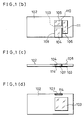
- FIG. 1(b) is a plan view showing electrodes of a coupled capacitor substrate of the frequency tunable resonator of FIG. 1(a).
- FIG. 1(c) is a side view of the coupled capacitor substrate of FIG. 1(b).
- FIG. 1(d) is a rear view of the coupled capacitor substrate of FIG. 1(b).
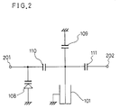
- FIG. 2 is an equivalent circuit diagram of the frequency tunable resonator of the first embodiment of the present invention.
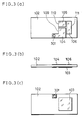
- FIG. 3(a) is a plan view showing a coupled capacitor substrate having another structure of the first embodiment of the present invention.
- FIG. 3(b) is a side view of the coupled capacitor substrate of FIG. 3(a).
- FIG. 3(c) is a rear view of the coupled capacitor substrate of FIG. 3(a).
- FIG. 4 is an exploded perspective view showing a frequency tunable resonator including a varactor of a second embodiment of the present invention.
- FIG. 5(a) is an exploded perspective view showing a frequency tunable resonator including a varactor of a third embodiment of the present invention.
- FIG. 5(b) is a plan view showing a coupled capacitor substrate of the frequency tunable resonator of FIG. 5(a).
- FIG. 5(c) is a side view of the coupled capacitor substrate of FIG. 5(b).
- FIG. 5(d) is a rear view of the coupled capacitor substrate of FIG. 5(b).
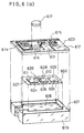
- FIG. 6(a) is an exploded perspective view showing a frequency tunable resonator including a varactor of a fourth embodiment of the present invention.
- FIG. 6(b) is a plan view showing a coupled capacitor substrate of the frequency tunable resonator of FIG. 6(a).
- FIG. 6(c) is a rear view showing the coupled capacitor substrate of FIG. 6(b).
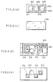
- FIG. 6(d) is a plan view showing a printed substrate for connecting external circuit.
- FIG. 6(e) is a rear view of the printed substrate of FIG. 6(d).
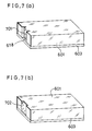
- FIG. 7(a) is a perspective view showing a rear face of the frequency tunable resonator of FIG. 6(a) for showing a first adjusting method.
- FIG. 7(b) is a perspective view showing a rear face of the resonator of FIG. 6(a) for showing a second adjusting method.
- FIG. 8 is the perspective view showing a conventional frequency tunable resonator including the varactor.
- FIG. 1(a) is an exploded perspective view showing a frequency tunable resonator including a varactor of the first embodiment of the present invention
- FIG. 1(b), FIG. 1(c) and FIG. 1(d) are respectively a plan view, a side view and a rear view showing electrodes of a coupled capacitor substrate of a frequency tunable resonator including a varactor shown in FIG. 1(a).
- the coupled capacitor substrate 102 is mounted on a planar type dielectric resonator 101, and electrodes 103, 104, 105 and 106 are provided on the coupled capacitor substrate 102. Furthermore, a side electrode 107 is provided on a side face of the coupled capacitor substrate 102, and a varactor 108 is fixed on the electrode 105.
- the planar type dielectric resonator 101 is made by plating and planning a metal, such as Cu (thickness: 6 -- 8 ⁇ m) or Ag (thickness: 10 ⁇ m), on a ceramic material block, such as barium titanate block.
- a plane capacitor 109 is constructed by the electrodes 103 and 104
- a plane capacitor 110 is constructed by the electrodes 103 and 105
- a plane capacitor 111 is constructed by the electrodes 103 and 106.
- the electrode 103 is connected to a strip line resonator electrode 112 of the planar type dielectric resonator 101
- the terminals of the varactor 108 are connected to the electrodes 104 and 105, respectively.
- an anode terminal of the varactor 108 is connected to the electrode 104
- a cathode terminal is connected to the electrode 105.
- the electrode 104 is connected via the side electrode 107 and a rear electrode 114 provided on the coupled capacitor substrate 102 to an electrode 113 of the planar type dielectric resonator so as to be grounded.
- the electrode 106 is connected to the oscillation circuit of the external oscillator (not shown).
- a reference numeral 115 indicates a grounded electrode.
- FIG. 2 shows an equivalent circuit diagram to the above-mentioned frequency tunable resonator including the varactor 108 of the first embodiment, and corresponding parts to the parts of FIG. 1 are designated by the same reference numerals.
- reference numeral 201 denotes a voltage control terminal
- reference numeral 202 indicates an oscillation circuit connection terminal.
- the planar type dielectric resonator 101 is formed by short-circuiting at the end of a strip line resonator electrode 112 so as to have a length of a quarter-wavelength and has an infinite impedance at a resonance frequency.
- the varactor 108 varies its capacitance depending upon a D.C. applied voltage and can control an oscillation frequency of the oscillator by utilizing this capacitance variation.
- the plane capacitor 110 couples the varactor 108 with the planar type dielectric resonator 101, and a range of variation of oscillation frequencies which corresponds to variation of D.C. voltages applied to the varactor 108 can be varied by changing the capacitance of the plane capacitor 110.
- the plane capacitor 109 is electrically connected to an open end portion of the strip line resonator electrode 112 of the planar type dielectric resonator 101 and a grounded conductor 115, and operates to lower the resonance frequency.
- the plane capacitor 111 performs capacitive coupling between the planar type dielectric resonator 101 and the external oscillation circuit. That is, the plane capacitors 109, 110, and 111 perform the same function as that of the chip capacitors 86, 84 and 85 of the aforementioned conventional frequency tunable resonator shown in FIG. 8.
- the electrode 105 of the plane capacitor 110 serves as a voltage control terminal electrode
- the electrode 106 of the plane capacitor 111 serves as a connection terminal electrode for connecting the oscillation circuit.
- the plane capacitors 109, 110, and 111 are formed on the coupled capacitor substrate 102, and thus the frequency tunable resonator of the first embodiment of the invention can be miniaturized as compared with a conventional resonator using the chip capacitors.
- the rear electrode 103 of the plane capacitors 109, 110, and 111 are directly connected to the electrode 112 formed on the planar type dielectric resonator 101 by mechanical contacts, and the plane capacitors 109 and 110 are connected to the varactor 108 directly.
- the configuration of the first embodiment does not require a printed circuit on substrate as shown in FIG. 8. And an adverse effect due to an inductance in the wiring patterns of the printed substrate can be eliminated by the configuration of the embodiment.
- the planar type dielectric resonator 101, plane capacitors 109, 110, 111 and the varactor 108 are integrated into one unit, and hence the characteristics of the frequency tunable resonator including the varactor 108 can be measured by easy handling.
- dispersion or scattering of the oscillator's characteristic can be minimized by trimming the frequency tunable resonator including the varactor 108 before mounting it on a substrate having active elements, etc., in the oscillator (not shown).
- the productivity is improved.
- Frequency adjusting of the frequency tunable resonator including the varactor as a whole can be effected not only by trimming the strip line resonator electrode 112 of the dielectric resonator but also by varying the size of the electrodes 104, 105 and 106. Therefore a frequency adjusting range becomes wide and degradation of resonance Q caused by cutting the dielectric resonator can be reduced.
- the electrode 104 is electrically connected to the rear electrode 114 of the coupled capacitor substrate 102 via the side electrode 107. But instead, it may be connected via a plated through hole 301 provided on the coupled capacitor substrate 102 as shown in FIG. 3.
- FIG. 4 is an exploded perspective view showing a frequency tunable resonator including a varactor of the second embodiment of the present invention.
- the frequency tunable resonator comprises laminate type dielectric resonator block 401, a resonator electrode 402, a shield electrode 403, capacitor electrodes 404, 405 and 406 forming capacitors, a side grounded electrode 407 for connecting the short-circuit side of the resonator electrode 402 to the shield electrode 403 to be grounded, and a varactor 408.
- the terminals of the varactor 408 are connected to the capacitor electrode 404 and the capacitor electrode 405, respectively.
- an anode terminal of the varactor 408 is connected to the capacitor electrode 404, and a cathode terminal is connected to the capacitor electrode 405.
- the capacitor electrode 405 is connected to a voltage control terminal 415 and supplied with a control voltage from an external unit.
- the capacitor electrode 404 is connected via a side-face-grounded electrode 412 to the shield electrode 403 to be grounded; and the capacitor electrode 406 is connected via an oscillation circuit connection electrode 416 to an external oscillation circuit (not shown).
- the difference of the second embodiment of FIG. 4 from the first embodiment of FIG. 1 resides in that the whole of the frequency tunable resonator is formed by a laminate structure. The other portions are almost the same.
- FIG. 4 An equivalent circuit of the frequency tunable resonator including the varactor 408 of the second embodiment is the same as that of FIG. 2, and thus the principle of operation of the circuit is almost the same as the first embodiment.
- the resonator electrode 402 is short-circuited at the end of strip line of substantially a quarter-wavelength, and the laminated dielectric resonator obtains the maximum impedance at a resonance frequency.
- the capacitor 410 couples the varactor 408 and the resonator electrode 402. A range of variation of oscillation frequencies which corresponds to variation of D.C.
- the capacitor 409 functions to lower a resonance frequency of the frequency tunable resonator of the second embodiment.
- the capacitor 411 capacitively couples the frequency tunable resonator and the oscillation circuit of an oscillator (not shown).
- the frequency tunable resonator of the second embodiment is constructed by the laminated structure, a thickness of a dielectric sheet 413 between the resonator electrode 402 and the capacitor electrode 404, 405 or 406 can be made so thin as 20 ⁇ m. Therefore, the capacitor 409, which lowers a resonance frequency of the frequency tunable resonator, can be made to have a large capacitance, thereby enabling to miniaturize the frequency tunable resonator. Furthermore, since the frequency tunable resonator and the capacitors are integrally formed, number of parts can be reduced.
- the whole of the frequency tunable resonator can be more miniaturized and thinned by employing the laminated structure. And the productivity can be improved by reducing number of parts and assembling hours. And further, the frequency tunable resonator of the second embodiment is suited for mass-production, because the frequency tunable resonator is constructed by the above-mentioned laminated structure.
- the frequency tunable resonator of the second embodiment may be so structured that another dielectric sheet is overlapped on the dielectric sheet 413 having electrodes as inner electrodes of the capacitors, and the capacitor electrodes 404 and 405 are extended to an upper face via the side-face-grounded electrode 412 of the lamination type dielectric resonator block 401 and the voltage control terminal electrode 415, and then the varactor 408 is mounted on these extended electrodes.
- FIG. 5(a) is an exploded perspective view showing a frequency tunable resonator including a varactor of the third embodiment of the present invention
- FIG. 5(b) is a plan view showing a coupled capacitor substrate 502.
- FIG. 5(c) is a side view of the coupled capacitor substrate 502 of FIG. 5(b).
- FIG. 5(d) is a bottom view of the coupled capacitor substrate 502 of FIG. 5(b).
- the frequency tunable resonator comprises a coaxial type dielectric resonator 501, a coupled capacitor substrate 502, electrodes 503, 504, 505 and 506 which are formed on the coupled capacitor substrate 502, a side electrode 507 which are formed on a side face of the coupled capacitor substrate 502 and a varactor 508.
- a plane capacitor 509 is constructed by the electrodes 503 and 504, a plane capacitor 510 is constructed by the electrodes 503 and 505, and a plane capacitor 511 is constructed by the electrodes 503 and 506.
- the electrode 503 is contacted to an inner conductor connection electrode 512 which is formed on an open end face of the coaxial type dielectric resonator 501 as shown in FIG. 5(a).
- the terminals of the varactor 508 are connected to the electrodes 504 and 505, respectively.
- an anode terminal of the varactor 508 is connected to the electrode 504, and a cathode terminal is connected to the electrode 505.
- the electrode 504 is connected via the side electrode 507 and a rear electrode 514 formed on the coupled capacitor substrate 502 as shown in FIG. 5(d), to an outer conductor connection electrode 513 to be grounded, and the electrode 506 is connected to an oscillation (not shown).
- a difference of the third embodiment of FIGs. 5(a), 5(b), 5(c) and 5(d) from the first embodiment of FIG. 1 resides in that the dielectric resonator is changed from the planar type dielectric resonator 101 to the coaxial type dielectric resonator 501.
- the other parts are almost the same as of FIG. 1.
- the coaxial type dielectric resonator 501 is obtained by short-circuiting at the end of a coaxial line (transmission line) of substantially a quarter-wavelength, and has an infinite impedance at a resonance frequency.
- a resonator having a higher Q value than that of a planar type dielectric resonator can be obtained by using a coaxial dielectric resonator.
- the varactor 508 varies its own capacitance depending upon a D.C. applied voltage, and thus an oscillation frequency of an oscillator can be adjusted by utilizing this capacitance variation.
- the plane capacitor 510 couples the varactor 508 and coaxial type dielectric resonator 501, and thus a range of variation of oscillation frequencies which corresponds to variation of D.C. voltages applied to the varactor 508 can be varied by changing the capacitance of the plane capacitor 510.
- the plane capacitor 509 is connected to an open end of the inner conductor connection electrode 512 of the coaxial type dielectric resonator 501 and a grounded conductor 513 and operates to lower a resonance frequency.
- the plane capacitor 511 capacitively couples the coaxial type dielectric resonator 501 and the external oscillation circuit.
- the electrode 505 serves as a voltage control terminal electrode, and the electrode 506 also serves as an oscillation circuit connection terminal electrode.
- this third embodiment can realize a frequency tunable resonator including a varactor which has a high Q value by employing a coaxial type dielectric resonator as the resonator.
- the electrode 504 is connected to the rear electrode 514 of the coupled capacitor substrate 502 via the side electrode 507; but alternatively it may be connected via a plated through hole.
- FIG. 6(a) is an exploded perspective view showing a frequency tunable resonator including a varactor of the fourth embodiment of the present invention.
- FIG. 6(b) is a plan view showing a coupled capacitor substrate 602
- FIG. 6(c) is a rear view showing the coupled capacitor substrate 602.
- FIG. 6(d) is a plan view showing a printed substrate 603.
- FIG. 6(e) is a rear view of the printed substrate 603.
- the frequency tunable resonator of this fourth embodiment comprises a planar type dielectric resonator 601, the coupled capacitor substrate 602, the printed substrate 603 for connecting of an external circuit, electrodes 604, 605, 606 and 607 which are formed on the coupled capacitor substrate 602, and a varactor 608.
- a plane capacitor 609 is constructed by the electrodes 604 and 605, a plane capacitor 610 is constructed by the electrodes 604 and 606, and a plane capacitor 611 is constructed by the electrodes 604 and 607.
- Each terminal electrode 612, 613 or 614 having plated through hole is formed on the printed substrate 603 with an electrode pattern 615.
- a through hole 616 is provided in the printed substrate 603 and sealed with hermetic material 617.
- a reference numeral 618 denotes a strip line resonator electrode having a recess shape which is formed over a recess-bottom face and recess-side faces of the planar type dielectric resonator 601.
- the strip line resonator electrode 618 is short-circuit portion to a grounded electrode 619 on a lower face of the planar type dielectric resonator 601.
- the electrode 604 is contacted to the strip line resonator electrode 618, and the terminals of the varactor 608 are connected to the electrodes 606 and 607, respectively.
- an anode terminal of the varactor 608 is connected to the electrode 606, and a cathode terminal is connected to the electrode 607.
- the electrode 605 is connected via a plated through hole to the oscillation circuit connection terminal electrode 612 on the printed substrate 603, and the electrode 606 is connected via the plated through hole to the terminal electrode 613 for grounding, and the electrode 607 is connected via the plated through hole to the voltage control terminal electrode 614.
- a reference numeral 620 denotes a connecting wire at the varactor 608.
- a difference of the fourth embodiment of FIGs. 6(a), 6(b), 6(c), 6(d) and 6(e) from the first embodiment of FIG. 1 resides in that the electrode portion of the planar type dielectric resonator 601 is provided in the recess, in which the coupled capacitor substrate 602 is placed, and furthermore the printed substrate 603 for connecting to a circuit (not shown) is bonded together with the planar type dielectric resonator so as to be formed into an integration.
- the other parts are almost the same as of FIG. 1.
- the planar type dielectric resonator 601 is obtained by short-circuiting at the end of a strip line of substantially a quarter-wavelength and realizes an infinite impedance at a resonance frequency.
- the plane capacitor 611 couples the varactor 608 and the planar type dielectric resonator 601.
- a range of variation of oscillation frequencies which corresponds to variation of D.C. voltages applied to the varactor 608 can be varied by changing the capacitance of the plane capacitor 611.
- the plane capacitor 610 is connected to an open end portion of the strip line resonator electrode 618 of the planar type dielectric resonator 601 and the grounded terminal electrode 613 of the printed substrate 603, and operates to lower a resonance frequency.
- the plane capacitor 609 capacitively couples the planar type dielectric resonator 601 and the external oscillation circuit.
- the frequency tunable resonator including the varactor 608 is configured as a module of a unitary body having the terminal electrodes, and therefore this structure facilitates mounting of the resonator on another printed substrate.
- the electrodes of the plane capacitors and the terminal electrodes on the printed substrate 603 are contacted via the plated through holes formed in the printed substrate 603, these connection between the electrodes and terminal electrodes can be easily effected by inserting solder into the plated through holes of the printed substrate 603.
- the through hole 616 in a portion of the printed substrate 603 overlapping the varactor 608, the printed substrate 603 is prevented from contacting with the varactor 608 and the connecting wire 620. And connections between the varactor 608 and the electrodes on the coupled capacitor substrate 602 can be easily checked via the through hole 616. And furthermore, by sealing the through hole 616 with hermetic material 617 such as resin, imperfect contact between the varactor 608 and electrodes can be prevented and durability of the frequency tunable resonator as a module is improved.
- hermetic material 617 such as resin
- the electrodes 606 and 607 of the plane capacitors can be contacted directly through the through hole 616, therefore a connection test between the electrodes 606 and 607 and the terminal electrode 613 and 614 can be performed easily.
- a resonance frequency or a range of variation of resonance frequencies can be adjusted by cutting the electrode of the plane capacitor.
- an electrode pattern as shown in FIG. 6(a) can be formed anywhere on the printed substrate 603, and therefore a device such as a high frequency choke coil circuit using a coil electrode pattern, which has been conventionally formed on an external circuit substrate, can be formed on a printed substrate as a module. Thus miniaturization of the device can be realized.
- the resonator electrode 618 on the planar type dielectric resonator 601 is formed into the recess-shape strip line, and a line width is made wide on the open end portion and narrow on the short-circuit end portion. Therefore, positioning of the planar type dielectric resonator 601 and the coupled capacitor substrate 602 can be performed easily by dropping the coupled capacitor substrate 602 into the recess of the open end portion, and this construction improves the productivity. Furthermore, decrease of electrode width on the short-circuit end portion of the resonator electrode 618 leads to increase of an equivalent line length of the strip line, and hence miniaturization of the planer type dielectric resonator 601. Furthermore, the forming of the resonator electrode 618 both over the upper face and the side face of the planer type dielectric resonator 601 leads to further miniaturization of the dielectric resonator is realized.
- FIG. 7 which is a rear view of an adjusted frequency tunable resonator including a varactor after assembling
- side electrode of the resonator electrode 618 is exposed outward, and therefore, by cutting this portion 701, an equivalent line length of the strip line can be increased so as to lower a resonance frequency, or as shown in FIG. 7(b), by heaping up some solder 702, the equivalent line length can be decreased so as to raise the resonance frequency.
- resonant frequency can be adjusted after assembling a module of the frequency tunable resonator including the varactor.
- a modified embodiment may be such that a frequency tunable resonator including a varactor can be applied to a high frequency filter or the like besides a high frequency oscillator.
Landscapes
- Inductance-Capacitance Distribution Constants And Capacitance-Resistance Oscillators (AREA)
Applications Claiming Priority (4)
| Application Number | Priority Date | Filing Date | Title |
|---|---|---|---|
| JP25954592A JP2853480B2 (ja) | 1992-09-29 | 1992-09-29 | バラクタ装荷共振器 |
| JP259545/92 | 1992-09-29 | ||
| JP131789/93 | 1993-06-02 | ||
| JP05131789A JP3141626B2 (ja) | 1993-06-02 | 1993-06-02 | バラクタ装荷共振器 |
Publications (2)
| Publication Number | Publication Date |
|---|---|
| EP0590612A1 true EP0590612A1 (de) | 1994-04-06 |
| EP0590612B1 EP0590612B1 (de) | 1998-08-26 |
Family
ID=26466524
Family Applications (1)
| Application Number | Title | Priority Date | Filing Date |
|---|---|---|---|
| EP93115651A Expired - Lifetime EP0590612B1 (de) | 1992-09-29 | 1993-09-28 | Frequenzabstimmbarer Resonator mit einem Varaktor |
Country Status (3)
| Country | Link |
|---|---|
| US (1) | US5475350A (de) |
| EP (1) | EP0590612B1 (de) |
| DE (1) | DE69320576T2 (de) |
Cited By (3)
| Publication number | Priority date | Publication date | Assignee | Title |
|---|---|---|---|---|
| EP0877437A1 (de) * | 1997-05-07 | 1998-11-11 | Murata Manufacturing Co., Ltd. | Streifenleitungsresonator und variabler Resonator |
| EP1119069A3 (de) * | 2000-01-18 | 2002-12-18 | Murata Manufacturing Co., Ltd. | Dielektrisches Filter, Einrichtung zur Antennenteilung und Kommunikationsgerät |
| WO2003028146A1 (en) * | 2001-09-27 | 2003-04-03 | Qualcomm Incorporated | Electrically tunable bandpass filters |
Families Citing this family (8)
| Publication number | Priority date | Publication date | Assignee | Title |
|---|---|---|---|---|
| FI97754C (fi) * | 1994-12-21 | 1997-02-10 | Verdera Oy | Resonaattorin resonanssitaajuuden sähköinen säätö |
| US6192752B1 (en) * | 1995-08-04 | 2001-02-27 | Zevex, Inc. | Noninvasive electromagnetic fluid level sensor |
| JPH1032429A (ja) * | 1996-07-18 | 1998-02-03 | Matsushita Electric Ind Co Ltd | 電圧制御共振器およびその調整方法 |
| JP3574893B2 (ja) * | 1999-10-13 | 2004-10-06 | 株式会社村田製作所 | 誘電体フィルタ、誘電体デュプレクサおよび通信装置 |
| US7268634B2 (en) * | 2004-08-27 | 2007-09-11 | The Hong Kong University Of Science And Technology | Dual-mode voltage controlled oscillator using integrated variable inductors |
| US7805978B2 (en) | 2006-10-24 | 2010-10-05 | Zevex, Inc. | Method for making and using an air bubble detector |
| WO2009029533A1 (en) | 2007-08-24 | 2009-03-05 | Zevex, Inc. | Ultrasonic air and fluid detector |
| WO2010091314A2 (en) | 2009-02-06 | 2010-08-12 | Zevex, Inc. | Air bubble detector |
Citations (4)
| Publication number | Priority date | Publication date | Assignee | Title |
|---|---|---|---|---|
| EP0069431A2 (de) * | 1981-07-08 | 1983-01-12 | CISE- Centro Informazioni Studi Esperienze S.p.A. | Planarer Oszillator mit dielektrischem Resonator für den Mikrowellenbereich |
| US4721932A (en) * | 1987-02-25 | 1988-01-26 | Rockwell International Corporation | Ceramic TEM resonator bandpass filters with varactor tuning |
| EP0444948A2 (de) * | 1990-03-02 | 1991-09-04 | Fujitsu Limited | Dielektrischer Resonator und Filter mit einem solchen Resonator |
| US5097237A (en) * | 1989-08-14 | 1992-03-17 | Oki Electric Industry Co., Ltd. | Microstrip line type resonator |
Family Cites Families (11)
| Publication number | Priority date | Publication date | Assignee | Title |
|---|---|---|---|---|
| JPS6390901A (ja) * | 1986-10-06 | 1988-04-21 | Matsushita Electric Ind Co Ltd | 電圧制御フイルタ |
| FR2614150A1 (fr) * | 1987-04-15 | 1988-10-21 | Alcatel Thomson Faisceaux | Oscillateur a resonateur dielectrique et accord electronique de frequence par varactor, notamment dans la gamme des 22 ghz |
| JPH0793535B2 (ja) * | 1988-01-25 | 1995-10-09 | 松下電器産業株式会社 | バラクタ装荷誘電体共振器と電圧制御型発振器 |
| JPH0644681B2 (ja) * | 1988-11-21 | 1994-06-08 | 国際電気株式会社 | 帯域阻止フィルタ |
| JPH0334608A (ja) * | 1989-06-30 | 1991-02-14 | Oki Electric Ind Co Ltd | マイクロ波帯誘電体電圧制御発振器 |
| JP3159445B2 (ja) * | 1990-11-27 | 2001-04-23 | 松下電器産業株式会社 | 高周波発振装置 |
| JPH04213204A (ja) * | 1990-12-10 | 1992-08-04 | Fujitsu Ltd | 共振回路及び共振周波数調整方法 |
| JP3088021B2 (ja) * | 1990-12-20 | 2000-09-18 | 株式会社村田製作所 | 電圧制御発振器 |
| JP3402369B2 (ja) * | 1991-11-11 | 2003-05-06 | ティーディーケイ株式会社 | 発振器モジュール |
| JPH04358408A (ja) * | 1991-06-04 | 1992-12-11 | Fujitsu Ltd | 共振回路及びその共振回路を使用した電圧制御発振器 |
| JP2949200B2 (ja) * | 1992-02-19 | 1999-09-13 | 住友金属工業株式会社 | 電圧制御発振器の周波数調整方法 |
-
1993
- 1993-09-28 US US08/127,500 patent/US5475350A/en not_active Expired - Lifetime
- 1993-09-28 DE DE69320576T patent/DE69320576T2/de not_active Expired - Lifetime
- 1993-09-28 EP EP93115651A patent/EP0590612B1/de not_active Expired - Lifetime
Patent Citations (4)
| Publication number | Priority date | Publication date | Assignee | Title |
|---|---|---|---|---|
| EP0069431A2 (de) * | 1981-07-08 | 1983-01-12 | CISE- Centro Informazioni Studi Esperienze S.p.A. | Planarer Oszillator mit dielektrischem Resonator für den Mikrowellenbereich |
| US4721932A (en) * | 1987-02-25 | 1988-01-26 | Rockwell International Corporation | Ceramic TEM resonator bandpass filters with varactor tuning |
| US5097237A (en) * | 1989-08-14 | 1992-03-17 | Oki Electric Industry Co., Ltd. | Microstrip line type resonator |
| EP0444948A2 (de) * | 1990-03-02 | 1991-09-04 | Fujitsu Limited | Dielektrischer Resonator und Filter mit einem solchen Resonator |
Cited By (7)
| Publication number | Priority date | Publication date | Assignee | Title |
|---|---|---|---|---|
| EP0877437A1 (de) * | 1997-05-07 | 1998-11-11 | Murata Manufacturing Co., Ltd. | Streifenleitungsresonator und variabler Resonator |
| EP1119069A3 (de) * | 2000-01-18 | 2002-12-18 | Murata Manufacturing Co., Ltd. | Dielektrisches Filter, Einrichtung zur Antennenteilung und Kommunikationsgerät |
| US6885261B2 (en) | 2000-01-18 | 2005-04-26 | Murata Manufacturing Co., Ltd. | Dielectric filter, antenna sharing device, and communication device having a voltage controlled reactance element for tuning the center frequency |
| WO2003028146A1 (en) * | 2001-09-27 | 2003-04-03 | Qualcomm Incorporated | Electrically tunable bandpass filters |
| EP2164129A1 (de) * | 2001-09-27 | 2010-03-17 | Qualcom Incorporated | Elektrisch abstimmbare Bandpassfilter |
| EP2309586A1 (de) * | 2001-09-27 | 2011-04-13 | Qualcomm Incorporated | Elektrisch abstimmbare Bandpassfilter |
| KR101036117B1 (ko) * | 2001-09-27 | 2011-05-23 | 퀄컴 인코포레이티드 | 전기적으로 튜닝가능한 대역통과필터 |
Also Published As
| Publication number | Publication date |
|---|---|
| DE69320576D1 (de) | 1998-10-01 |
| DE69320576T2 (de) | 1999-01-14 |
| EP0590612B1 (de) | 1998-08-26 |
| US5475350A (en) | 1995-12-12 |
Similar Documents
| Publication | Publication Date | Title |
|---|---|---|
| KR0147726B1 (ko) | 유전체 필터 | |
| US5764118A (en) | Dielectric coaxial filter with irregular polygon shaped recesses | |
| US5475350A (en) | Frequency tunable resonator including a varactor | |
| US6941650B2 (en) | Method for manufacturing dielectric laminated device | |
| US6294968B1 (en) | Dielectric filter and process for producing same | |
| JPH10215119A (ja) | 電圧制御発振器 | |
| US6166613A (en) | Voltage-controlled resonator, method of fabricating the same, method of tuning the same, and mobile communication apparatus | |
| JPH03254201A (ja) | 誘電体帯域阻止フィルタ | |
| JP3464820B2 (ja) | 誘電体積層共振器および誘電体フィルタ | |
| EP0324453A2 (de) | Filter mit verteilten Impedanzelementen | |
| JP3141626B2 (ja) | バラクタ装荷共振器 | |
| US6392505B1 (en) | Dielectric device | |
| JPH06112711A (ja) | バラクタ装荷共振器 | |
| JP3368404B2 (ja) | 共振器およびフィルタ | |
| EP0113793B1 (de) | Koaxialer Resonator | |
| JP2666094B2 (ja) | 誘電体帯域阻止フィルタ | |
| JP2661004B2 (ja) | 誘電体フィルタ | |
| JPH0621706A (ja) | トリプレート型共振器および超高周波機能部品 | |
| JPH05110319A (ja) | トリプレート形ストリツプライン共振器 | |
| JP2900736B2 (ja) | インピーダンス変換素子 | |
| JPH0897607A (ja) | 誘電体フィルタ用基板 | |
| JPH06169201A (ja) | 積層型誘電体有極フィルタ | |
| JPH0744367B2 (ja) | 誘電体フィルタの入出力結合構造 | |
| JPH09294002A (ja) | 誘電体フィルタ | |
| JP2001267825A (ja) | アンテナ装置 |
Legal Events
| Date | Code | Title | Description |
|---|---|---|---|
| PUAI | Public reference made under article 153(3) epc to a published international application that has entered the european phase |
Free format text: ORIGINAL CODE: 0009012 |
|
| AK | Designated contracting states |
Kind code of ref document: A1 Designated state(s): DE FR GB |
|
| 17P | Request for examination filed |
Effective date: 19940414 |
|
| 17Q | First examination report despatched |
Effective date: 19960429 |
|
| GRAG | Despatch of communication of intention to grant |
Free format text: ORIGINAL CODE: EPIDOS AGRA |
|
| GRAG | Despatch of communication of intention to grant |
Free format text: ORIGINAL CODE: EPIDOS AGRA |
|
| GRAH | Despatch of communication of intention to grant a patent |
Free format text: ORIGINAL CODE: EPIDOS IGRA |
|
| GRAH | Despatch of communication of intention to grant a patent |
Free format text: ORIGINAL CODE: EPIDOS IGRA |
|
| GRAA | (expected) grant |
Free format text: ORIGINAL CODE: 0009210 |
|
| AK | Designated contracting states |
Kind code of ref document: B1 Designated state(s): DE FR GB |
|
| REF | Corresponds to: |
Ref document number: 69320576 Country of ref document: DE Date of ref document: 19981001 |
|
| ET | Fr: translation filed | ||
| PLBE | No opposition filed within time limit |
Free format text: ORIGINAL CODE: 0009261 |
|
| STAA | Information on the status of an ep patent application or granted ep patent |
Free format text: STATUS: NO OPPOSITION FILED WITHIN TIME LIMIT |
|
| 26N | No opposition filed | ||
| REG | Reference to a national code |
Ref country code: GB Ref legal event code: IF02 |
|
| PGFP | Annual fee paid to national office [announced via postgrant information from national office to epo] |
Ref country code: GB Payment date: 20120926 Year of fee payment: 20 |
|
| PGFP | Annual fee paid to national office [announced via postgrant information from national office to epo] |
Ref country code: FR Payment date: 20120926 Year of fee payment: 20 Ref country code: DE Payment date: 20120927 Year of fee payment: 20 |
|
| REG | Reference to a national code |
Ref country code: DE Ref legal event code: R071 Ref document number: 69320576 Country of ref document: DE |
|
| REG | Reference to a national code |
Ref country code: GB Ref legal event code: PE20 Expiry date: 20130927 |
|
| PG25 | Lapsed in a contracting state [announced via postgrant information from national office to epo] |
Ref country code: GB Free format text: LAPSE BECAUSE OF EXPIRATION OF PROTECTION Effective date: 20130927 |
|
| PG25 | Lapsed in a contracting state [announced via postgrant information from national office to epo] |
Ref country code: DE Free format text: LAPSE BECAUSE OF EXPIRATION OF PROTECTION Effective date: 20131001 |