EP0593729B1 - Analog digitalwandler und einen solchen analog digitalwandler benutzenderegelschleife. - Google Patents
Analog digitalwandler und einen solchen analog digitalwandler benutzenderegelschleife. Download PDFInfo
- Publication number
- EP0593729B1 EP0593729B1 EP93910096A EP93910096A EP0593729B1 EP 0593729 B1 EP0593729 B1 EP 0593729B1 EP 93910096 A EP93910096 A EP 93910096A EP 93910096 A EP93910096 A EP 93910096A EP 0593729 B1 EP0593729 B1 EP 0593729B1
- Authority
- EP
- European Patent Office
- Prior art keywords
- voltage
- converter
- levels
- level
- analogue
- Prior art date
- Legal status (The legal status is an assumption and is not a legal conclusion. Google has not performed a legal analysis and makes no representation as to the accuracy of the status listed.)
- Expired - Lifetime
Links
- 230000006641 stabilisation Effects 0.000 claims description 2
- 238000011105 stabilization Methods 0.000 claims description 2
- 230000001131 transforming effect Effects 0.000 abstract description 2
- 238000006243 chemical reaction Methods 0.000 description 10
- 230000010355 oscillation Effects 0.000 description 3
- 238000000034 method Methods 0.000 description 2
- 238000005070 sampling Methods 0.000 description 2
- 230000003321 amplification Effects 0.000 description 1
- 238000003199 nucleic acid amplification method Methods 0.000 description 1
- 230000003071 parasitic effect Effects 0.000 description 1
- 238000011002 quantification Methods 0.000 description 1
- 238000013139 quantization Methods 0.000 description 1
- 229910052710 silicon Inorganic materials 0.000 description 1
- 239000010703 silicon Substances 0.000 description 1
Images


Classifications
-
- H—ELECTRICITY
- H04—ELECTRIC COMMUNICATION TECHNIQUE
- H04N—PICTORIAL COMMUNICATION, e.g. TELEVISION
- H04N5/00—Details of television systems
- H04N5/14—Picture signal circuitry for video frequency region
- H04N5/16—Circuitry for reinsertion of DC and slowly varying components of signal; Circuitry for preservation of black or white level
-
- H—ELECTRICITY
- H03—ELECTRONIC CIRCUITRY
- H03M—CODING; DECODING; CODE CONVERSION IN GENERAL
- H03M1/00—Analogue/digital conversion; Digital/analogue conversion
- H03M1/12—Analogue/digital converters
- H03M1/14—Conversion in steps with each step involving the same or a different conversion means and delivering more than one bit
- H03M1/144—Conversion in steps with each step involving the same or a different conversion means and delivering more than one bit the steps being performed sequentially in a single stage, i.e. recirculation type
-
- H—ELECTRICITY
- H03—ELECTRONIC CIRCUITRY
- H03M—CODING; DECODING; CODE CONVERSION IN GENERAL
- H03M1/00—Analogue/digital conversion; Digital/analogue conversion
- H03M1/12—Analogue/digital converters
- H03M1/34—Analogue value compared with reference values
- H03M1/36—Analogue value compared with reference values simultaneously only, i.e. parallel type
- H03M1/361—Analogue value compared with reference values simultaneously only, i.e. parallel type having a separate comparator and reference value for each quantisation level, i.e. full flash converter type
Definitions
- the present invention relates to an analog-digital converter.
- Analog to digital converters are used in electronics when digital coding of information occurs.
- ADC analog-digital converter
- This analog electrical quantity can be either a voltage or a current.
- an analog-digital converter of n bits delivers 2 n combinations each having n bits of resolution.
- the accuracy of such a converter is given by the switching of the least significant bit, noted LSB (Least Significant Bit).
- LSB least Significant Bit
- the aim of the DC component restoring operation is to set the reference DC voltage of the video signal to a precise value.
- the video signal of each line is sampled on its DC component or black level. A fraction of each sample is taken and compared to a reference value so as to generate an error signal which is fed back, possibly after amplification, into the video signal.
- the continuous level taken at the output of the analog-digital converter is then defined with an accuracy of ⁇ 1 LSB.
- the DC component then has an oscillation of ⁇ 1 bit of quantification around the setpoint, which has the consequence of preventing its stabilization.
- the invention does not have this drawback.
- the present invention relates to an analog-digital voltage converter comprising 2 n - 1 comparators making it possible to generate 2 n different voltage levels when the input voltage varies, and a binary coding circuit comprising means for transforming the 2 n voltage levels in 2 n binary codes each having n resolution bits, characterized in that it comprises additional means making it possible to code the voltage contained in at least one range of variation of the input voltage into information having a number bit resolution higher than n.
- the present invention also relates to a loop for controlling the DC component of a video signal, characterized in that it contains an analog-digital converter according to the invention.
- An advantage of the invention is therefore to correctly stabilize the level of the DC component.
- the analog input electrical quantity is a voltage
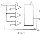
- FIG. 1 describes an analog-digital converter 100 according to the prior art. It is a converter known to those skilled in the art under the name of flash converter. For reasons of simplification, the device shown in FIG. 1 is a 2-bit converter delivering 4 combinations. As is known to a person skilled in the art, this converter contains 3 comparators 1. In general, a n-bit flash type converter contains 2 n - 1 comparators.
- the converter of FIG. 1 is such that the analog input voltage V is compared with 3 reference voltages V1, V2, V3 using 3 comparators.
- the signal from each comparator takes a first value or a second value from two possible values.
- the different signals from the comparators are then sent in a logic circuit 2 allowing, as is known to those skilled in the art, to binary code the information it receives in the form of 2-bit combinations.
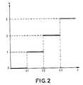
- Figure 2 describes the converter conversion curve described in Figure 1.
- This curve associates the input voltage V with the binary codes by the rows or levels N which make it possible to symbolize them. It is then possible to draw up the following table:
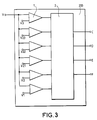
- FIG. 3 represents an example of an analog-digital converter according to an embodiment of the invention.
- the converter 200 described in FIG. 3 contains 3 comparators associated with the respective voltages V1, V2, V3.
- a binary coding logic circuit 2 collects the signals from the different comparators.
- the binary codes generated by circuit 2 are combinations of 4 bits collected respectively at points C, D, E, F.
- Figure 4 describes the conversion curve of the converter in Figure 3.
- the precision of the converter is multiplied by 4 when the analog voltage V varies between V2 and V3 since the converter delivers two additional resolution bits.
- the binary codes collected at points C and D of the converter 200 are identical to the binary codes collected respectively at points A and B of the converter 100.
- the binary codes collected at points E and F are associated with the information delivered by the 3 additional comparators. These comparators make it possible to generate 4 combinations of 2 bits each when the voltage V is between the values V2 and V3.
- the logic circuit 2 forces the bits to zero by any means known to those skilled in the art and which it is therefore not necessary to recall in the present application .
- FIG. 5 represents an analog-digital converter according to the preferred embodiment of the invention. This is the generalization of the analog-digital converter described in Figure 3.
- the converter 300 comprises q additional comparators 20.
- NI q + 1 intermediate levels located between level N o and level N o + 1.
- the binary coding circuit 2 converts on the one hand the information constituted by the 2 n levels into n-bit codes and, on the other hand, the information constituted by the NI intermediate levels in p-bit codes.
- the binary codes of n bits are collected on the outputs S1, S2 --- Sn, and the binary codes of p bits on the outputs S n + 1 , --- S n + p .
- the binary coding circuit comprises means making it possible to force to zero the combinations of the p bits for all the whole levels from 1 to 2 n , that is to say elsewhere than in the area of interest.
- the analog-digital converter which has just been described comprises a single subset of q additional comparators located between two successive whole levels. It is obvious that the invention also relates to analog-digital converters containing several subsets of additional comparators such as that described above.
- the additional levels generated by a subset of q comparators can be located between two successive whole levels, as described above, or on either side of one or more whole levels.
- FIG. 6 represents an application of the converter described in FIG. 5.
- the analog-digital converter 300 is located in a control loop of the DC component of a video signal Sv.
- the intermediate levels are then 3 in number (16.25, 16.50, 16.75).
- the combinations of the additional p bits are only significant for the non-integer intermediate levels (for example 16.25, 16.50 and 16.75 according to the preferred embodiment of the invention) because, as previously mentioned, the binary coding circuit 2 comprises means making it possible to force the combinations of p bits to zero for all the whole levels from 1 to 2 n , that is to say elsewhere than in the zone where the intermediate levels are of interest.
- the device of FIG. 6 makes it possible to slave the DC component of the video signal so as to suppress the oscillation of + 1 quantization bit which is present in the devices of the prior art.
- a command C1 makes it possible to sample the logic gatekeeper 3 at the rate of appearance of the black level of the input video signal Sv.
- the codes used around the DC component are then compared to using the comparator 4 to a reference code R1 whose combination is identical to one of those whose p-bit codes are significant.
- the error signal from the comparator 4 is then transferred using the loop filter 5, for example a digital integrator, to a digital analog converter 6 which transforms the digital error into an analog error voltage applied to the algebraic adder 7 so as to readjust the continuous level of the voltage.
- the loop filter 5 for example a digital integrator
- the reference code R1 is identical to that which corresponds to level 16.50.
- the precision obtained in steady state is given by the switching of the least significant bit.
- the precision obtained is therefore equal to ⁇ 0.25 LSB around the reference setpoint R1, where LSB designates the least significant bit of the n-bit codes.
- the continuous level of the video component is thus fixed at level 16, without parasitic oscillation.
- the precision of the analog-digital converter is equal to ⁇ 1 LSB / 2 P.
Landscapes
- Engineering & Computer Science (AREA)
- Theoretical Computer Science (AREA)
- Multimedia (AREA)
- Signal Processing (AREA)
- Analogue/Digital Conversion (AREA)
- Picture Signal Circuits (AREA)
Claims (5)
- Analog-Digital-Spannungswandler (300) mit 2n - 1 Vergleichern (1), die die Erzeugung von 2n unterschiedlichen Spannungspegeln erlauben, wenn die Eingangsspannung zwischen einem Mindest- und einem Höchstpegel schwankt, und einer binären Codierschaltung mit Mitteln zum Umformen der 2n Spannungspegel in 2n Binärcodes jeweils mit n Bit Auflösung, dadurch gekennzeichnet, daß er Zusatzmittel (20) umfaßt, die die Codierung der Gleichspannung in mindestens einem Bereich der Veränderung der Eingangsspannung zwischen dem Mindest- und dem Höchstpegel in eine Information mit einer Anzahl von Auflösungsbit erlauben, die höher als n ist, wobei der oder die besagten Bereiche der Spannungsveränderung nicht den gesamten Ausschlag der Eingangsspannung abdecken.
- Analog-Digital-Spannungswandler (300) nach Anspruch 1, dadurch gekennzeichnet, daß die Zusatzmittel mindestens eine Gruppe von 2p - 1 Vergleichern umfassen, die die Erzeugung von 2p Spannungspegeln zwischen einem ersten Pegel (No) und zweiten Pegel (No + 1) erlauben, wobei der besagte erste und zweite Pegel zwei aufeinanderfolgende, unter den 2n Pegeln gewählte Pegel sind, und daß die binäre Codierschaltung (2) Mittel zum Umformen der 2p Spannungspegel in 2p Binärcodes von jeweils p Bit umfaßt, so daß die Eingangsspannung in eine Kombination von n + p Bit umgewandelt wird, die aus den 2n + 2p, am Ausgang des Wandlers verfügbaren Kombinationen entnommen worden ist.
- Analog-Digital-Spannungswandler nach Anspruch 2, dadurch gekennzeichnet, daß die binäre Codierschaltung (2) Mittel zum Nullsetzen der p Bit der mit den 2n Spannungspegeln verbundenen 2n Kombinationen umfaßt.
- Regelschleife der Gleichkomponente eines Videosignals, dadurch gekennzeichnet, daß sie einen Analog-Digital-Spannungswandler nach einem der vorhergehenden Ansprüche enthält, der so beschaffen ist, daß der erste unter den 2n Pegeln gewählte Pegel (No) dem Stabilisierungspegel der besagten Gleichkomponente entspricht.
- Regelschleife nach Anspruch 4, dadurch gekennzeichnet, daß sie folgendes umfaßt: ein mit dem Digital-Analog-Wandler verbundenes Logikgatter (3), das die Abtastung des vom Wandler abgegebenen Signals im Raster des Erscheinens der Gleichkomponente unter dem Einfluß eines externen Befehls (C1) erlaubt, einen die vom Logikgatter (3) abgegebene Information aufnehmenden und die besagte Information mit einem Bezugscode (R1) vergleichenden Vergleicher (4), wobei die Kombination des Bezugscodes einer von denen gleich ist, deren p-Bit-Code nicht Null sind, einen das vom Vergleicher abgegebene Signal aufnehmenden Schleifenfilter (5), einen Analog-Digital-Wandler (6), der das vom Schleifenfilter (5) abgegebene Signal in eine analoge Fehlerspannung umformt, und einen algebraischen Summierer (7), der die analoge Fehlerspannung zur Neueinstellung des Pegels der Gleichkomponente aufnimmt.
Applications Claiming Priority (3)
| Application Number | Priority Date | Filing Date | Title |
|---|---|---|---|
| FR9205637 | 1992-05-07 | ||
| FR9205637A FR2691026B1 (fr) | 1992-05-07 | 1992-05-07 | Convertisseur analogique-numerique et boucle d'asservissement utilisant un tel convertisseur. |
| PCT/FR1993/000443 WO1993022840A1 (fr) | 1992-05-07 | 1993-05-07 | Convertisseur analogique-numerique et boucle d'asservissement utilisant un tel convertisseur |
Publications (2)
| Publication Number | Publication Date |
|---|---|
| EP0593729A1 EP0593729A1 (de) | 1994-04-27 |
| EP0593729B1 true EP0593729B1 (de) | 1996-11-06 |
Family
ID=9429626
Family Applications (1)
| Application Number | Title | Priority Date | Filing Date |
|---|---|---|---|
| EP93910096A Expired - Lifetime EP0593729B1 (de) | 1992-05-07 | 1993-05-07 | Analog digitalwandler und einen solchen analog digitalwandler benutzenderegelschleife. |
Country Status (8)
| Country | Link |
|---|---|
| US (1) | US5537114A (de) |
| EP (1) | EP0593729B1 (de) |
| JP (1) | JPH06508972A (de) |
| DE (1) | DE69305827T2 (de) |
| ES (1) | ES2096290T3 (de) |
| FR (1) | FR2691026B1 (de) |
| SG (1) | SG63638A1 (de) |
| WO (1) | WO1993022840A1 (de) |
Families Citing this family (6)
| Publication number | Priority date | Publication date | Assignee | Title |
|---|---|---|---|---|
| KR100265753B1 (ko) * | 1997-01-17 | 2000-10-02 | 윤종용 | 펜디지타이저제어장치및방법 |
| US5881776A (en) * | 1997-01-24 | 1999-03-16 | Safety Components Fabric Technologies, Inc. | Rapier woven low permeability air bag fabric |
| US6326935B1 (en) * | 1999-09-28 | 2001-12-04 | Gateway, Inc. | Method and apparatus for changing the mode of a display apparatus |
| US20040004608A1 (en) * | 2002-07-03 | 2004-01-08 | Kinpo Electronics, Inc. | Display device for reducing power consumption and protecting user's eyes |
| US7859441B2 (en) | 2007-04-11 | 2010-12-28 | Mediatek Inc. | Data readout system having non-uniform ADC resolution and method thereof |
| JP2010278557A (ja) * | 2009-05-26 | 2010-12-09 | Panasonic Corp | 並列補間型a/d変換器及びディジタル等化装置 |
Family Cites Families (13)
| Publication number | Priority date | Publication date | Assignee | Title |
|---|---|---|---|---|
| US3283319A (en) * | 1960-08-25 | 1966-11-01 | Nippon Electric Co | Code converter |
| US4217574A (en) * | 1976-08-09 | 1980-08-12 | Gte Laboratories Incorporated | Analog to digital converter having nonlinear amplitude transformation |
| USRE32313E (en) * | 1979-09-10 | 1986-12-23 | Hitachi, Ltd. | Digital-to-analog converter and PCM encoder using the converter |
| GB2082410B (en) * | 1980-08-23 | 1984-08-30 | Plessey Co Ltd | Analogue-to-digital converter |
| US4571574A (en) * | 1982-09-30 | 1986-02-18 | Witold Krynicki | Analogue to digital converter |
| JPS61120530A (ja) * | 1984-11-15 | 1986-06-07 | Toshiba Corp | アナログ・デジタル変換器 |
| FR2626423A1 (fr) * | 1988-01-21 | 1989-07-28 | Inst Francais Du Petrole | Dispositif d'acquisition pour la numerisation de signaux a grande dynamique |
| JPH0612879B2 (ja) * | 1988-03-08 | 1994-02-16 | ヤマハ株式会社 | 並列比較型アナログ・ディジタル変換器 |
| US5087973A (en) * | 1988-11-17 | 1992-02-11 | Matsushita Electric Industrial Co., Ltd. | Clamp signal processing apparatus |
| US5355135A (en) * | 1989-01-30 | 1994-10-11 | Linear Technology Corporation | Semi-flash A/D converter using switched capacitor comparators |
| JP2543177B2 (ja) * | 1989-03-24 | 1996-10-16 | 松下電器産業株式会社 | クランプ装置と自動利得制御装置 |
| JPH0456519A (ja) * | 1990-06-26 | 1992-02-24 | Mitsubishi Electric Corp | A/d変換器 |
| GB9205727D0 (en) * | 1992-03-16 | 1992-04-29 | Sarnoff David Res Center | Averaging,flash analog to digital converter |
-
1992
- 1992-05-07 FR FR9205637A patent/FR2691026B1/fr not_active Expired - Fee Related
-
1993
- 1993-05-07 WO PCT/FR1993/000443 patent/WO1993022840A1/fr not_active Ceased
- 1993-05-07 ES ES93910096T patent/ES2096290T3/es not_active Expired - Lifetime
- 1993-05-07 EP EP93910096A patent/EP0593729B1/de not_active Expired - Lifetime
- 1993-05-07 SG SG1996009325A patent/SG63638A1/en unknown
- 1993-05-07 DE DE69305827T patent/DE69305827T2/de not_active Expired - Lifetime
- 1993-05-07 JP JP5519019A patent/JPH06508972A/ja active Pending
- 1993-11-11 US US08/182,210 patent/US5537114A/en not_active Expired - Lifetime
Also Published As
| Publication number | Publication date |
|---|---|
| US5537114A (en) | 1996-07-16 |
| FR2691026A1 (fr) | 1993-11-12 |
| DE69305827T2 (de) | 1997-05-07 |
| DE69305827D1 (de) | 1996-12-12 |
| JPH06508972A (ja) | 1994-10-06 |
| SG63638A1 (en) | 1999-03-30 |
| ES2096290T3 (es) | 1997-03-01 |
| WO1993022840A1 (fr) | 1993-11-11 |
| FR2691026B1 (fr) | 1997-01-03 |
| EP0593729A1 (de) | 1994-04-27 |
Similar Documents
| Publication | Publication Date | Title |
|---|---|---|
| US6781533B2 (en) | Optically sampled delta-sigma modulator | |
| FR2642920A1 (fr) | Double convertisseur analogique-numerique avec un seul registre d'approximations successives et procede de conversion analogique-numerique | |
| US20110114842A1 (en) | Infrared photocurrent front-end ADC for rain-sensing system with ambient light compensation | |
| EP0887941B1 (de) | Anordnung zur Erzeugung von analogen Signalen unter Benutzung von Analog-Digitalwandlern, besonders für direkte digitale Synthese | |
| FR2586516A1 (fr) | Convertisseur analogique-numerique a conversion fractionnee comportant un circuit d'isolation entre un noeud de soustraction et un codeur de bits de faible poids | |
| FR2509048A1 (fr) | Dispositif transducteur de pression capacitif a caracteristique lineaire | |
| FR2689343A1 (fr) | Convertisseur analogique-numérique prédictif à action directe. | |
| FR2619268A1 (fr) | Convertisseur analogique-numerique a sous-gammes comportant un circuit d'isolation entre un noeud de soustraction et un codeur de bits de moindre poids | |
| EP0593729B1 (de) | Analog digitalwandler und einen solchen analog digitalwandler benutzenderegelschleife. | |
| FR2589649A1 (fr) | Dispositif destine a augmenter la puissance de sortie d'un appareil radioelectrique alimente a basse tension, par exemple du type autoradio | |
| FR2718585A1 (fr) | Modulateur avec codage amélioré. | |
| EP3843277A1 (de) | Analog-digital-wandlervorrichtung mit zwei kaskadierten analog-digital-wandlerstufen mit register mit sukzessiven approximationen, sowie entsprechender elektronischer sensor | |
| EP1039643A1 (de) | Analog-Digital-Wandleranordnung mit konstanter differentieller nicht-linearität | |
| FR2621434A1 (fr) | Convertisseur numerique a analogique avec compensation de la fonction de commutateur | |
| FR2604840A1 (fr) | Convertisseur analogique-numerique differentiel a capacites commutees | |
| FR2507413A1 (fr) | Convertisseur analogique-numerique ayant un circuit d'auto-polarisation | |
| FR2590092A1 (fr) | Convertisseur a/n ou n/a | |
| EP0161963A2 (de) | Ultraschneller Dichotomie-AD-Wandler | |
| FR2749455A1 (fr) | Convertisseur analogique-numerique du type parallele | |
| EP1192718A1 (de) | Verfahren und system zur kompensierung der nichtlinearität eines sigma-delta analog-digital-wandlers | |
| EP0834990A1 (de) | Programmierbarer digitaler Phasenschieber und Analog-Digital-Umsetzer damit | |
| EP0155046B1 (de) | Gerät zur Digital-Analogwandlung | |
| FR2873245A1 (fr) | Procede de traitement en mode differentiel d'une tension incidente relativement a une tension de reference et dispositif correspondant | |
| EP0305301A1 (de) | Signalkompressorschaltung, insbesondere für Fernsprechapparate | |
| EP0556927B1 (de) | Differenzschaltung mit hoher Linearität |
Legal Events
| Date | Code | Title | Description |
|---|---|---|---|
| PUAI | Public reference made under article 153(3) epc to a published international application that has entered the european phase |
Free format text: ORIGINAL CODE: 0009012 |
|
| 17P | Request for examination filed |
Effective date: 19931209 |
|
| AK | Designated contracting states |
Kind code of ref document: A1 Designated state(s): DE ES FR GB IT |
|
| GRAG | Despatch of communication of intention to grant |
Free format text: ORIGINAL CODE: EPIDOS AGRA |
|
| 17Q | First examination report despatched |
Effective date: 19960313 |
|
| GRAH | Despatch of communication of intention to grant a patent |
Free format text: ORIGINAL CODE: EPIDOS IGRA |
|
| GRAH | Despatch of communication of intention to grant a patent |
Free format text: ORIGINAL CODE: EPIDOS IGRA |
|
| GRAA | (expected) grant |
Free format text: ORIGINAL CODE: 0009210 |
|
| RAP1 | Party data changed (applicant data changed or rights of an application transferred) |
Owner name: THOMSON MULTIMEDIA |
|
| AK | Designated contracting states |
Kind code of ref document: B1 Designated state(s): DE ES FR GB IT |
|
| REF | Corresponds to: |
Ref document number: 69305827 Country of ref document: DE Date of ref document: 19961212 |
|
| ITF | It: translation for a ep patent filed | ||
| GBT | Gb: translation of ep patent filed (gb section 77(6)(a)/1977) |
Effective date: 19970122 |
|
| REG | Reference to a national code |
Ref country code: ES Ref legal event code: FG2A Ref document number: 2096290 Country of ref document: ES Kind code of ref document: T3 |
|
| PLBE | No opposition filed within time limit |
Free format text: ORIGINAL CODE: 0009261 |
|
| STAA | Information on the status of an ep patent application or granted ep patent |
Free format text: STATUS: NO OPPOSITION FILED WITHIN TIME LIMIT |
|
| 26N | No opposition filed | ||
| REG | Reference to a national code |
Ref country code: GB Ref legal event code: 746 Effective date: 20011126 |
|
| REG | Reference to a national code |
Ref country code: GB Ref legal event code: IF02 |
|
| REG | Reference to a national code |
Ref country code: FR Ref legal event code: D6 |
|
| PGFP | Annual fee paid to national office [announced via postgrant information from national office to epo] |
Ref country code: ES Payment date: 20080619 Year of fee payment: 16 |
|
| PGFP | Annual fee paid to national office [announced via postgrant information from national office to epo] |
Ref country code: IT Payment date: 20080528 Year of fee payment: 16 |
|
| REG | Reference to a national code |
Ref country code: ES Ref legal event code: FD2A Effective date: 20090508 |
|
| PG25 | Lapsed in a contracting state [announced via postgrant information from national office to epo] |
Ref country code: ES Free format text: LAPSE BECAUSE OF NON-PAYMENT OF DUE FEES Effective date: 20090508 |
|
| PG25 | Lapsed in a contracting state [announced via postgrant information from national office to epo] |
Ref country code: IT Free format text: LAPSE BECAUSE OF NON-PAYMENT OF DUE FEES Effective date: 20090507 |
|
| PGFP | Annual fee paid to national office [announced via postgrant information from national office to epo] |
Ref country code: DE Payment date: 20120529 Year of fee payment: 20 |
|
| PGFP | Annual fee paid to national office [announced via postgrant information from national office to epo] |
Ref country code: GB Payment date: 20120525 Year of fee payment: 20 Ref country code: FR Payment date: 20120607 Year of fee payment: 20 |
|
| REG | Reference to a national code |
Ref country code: DE Ref legal event code: R071 Ref document number: 69305827 Country of ref document: DE |
|
| REG | Reference to a national code |
Ref country code: GB Ref legal event code: PE20 Expiry date: 20130506 |
|
| PG25 | Lapsed in a contracting state [announced via postgrant information from national office to epo] |
Ref country code: DE Free format text: LAPSE BECAUSE OF EXPIRATION OF PROTECTION Effective date: 20130508 Ref country code: GB Free format text: LAPSE BECAUSE OF EXPIRATION OF PROTECTION Effective date: 20130506 |