EP0594300A1 - Méthode pour la fabrication d'un contact à métal - Google Patents
Méthode pour la fabrication d'un contact à métal Download PDFInfo
- Publication number
- EP0594300A1 EP0594300A1 EP93307350A EP93307350A EP0594300A1 EP 0594300 A1 EP0594300 A1 EP 0594300A1 EP 93307350 A EP93307350 A EP 93307350A EP 93307350 A EP93307350 A EP 93307350A EP 0594300 A1 EP0594300 A1 EP 0594300A1
- Authority
- EP
- European Patent Office
- Prior art keywords
- layer
- aluminum
- aluminum layer
- forming
- deposited
- Prior art date
- Legal status (The legal status is an assumption and is not a legal conclusion. Google has not performed a legal analysis and makes no representation as to the accuracy of the status listed.)
- Granted
Links
Images
Classifications
-
- H—ELECTRICITY
- H10—SEMICONDUCTOR DEVICES; ELECTRIC SOLID-STATE DEVICES NOT OTHERWISE PROVIDED FOR
- H10W—GENERIC PACKAGES, INTERCONNECTIONS, CONNECTORS OR OTHER CONSTRUCTIONAL DETAILS OF DEVICES COVERED BY CLASS H10
- H10W20/00—Interconnections in chips, wafers or substrates
- H10W20/01—Manufacture or treatment
- H10W20/031—Manufacture or treatment of conductive parts of the interconnections
- H10W20/032—Manufacture or treatment of conductive parts of the interconnections of conductive barrier, adhesion or liner layers
- H10W20/042—Manufacture or treatment of conductive parts of the interconnections of conductive barrier, adhesion or liner layers the barrier, adhesion or liner layers being seed or nucleation layers
- H10W20/045—Manufacture or treatment of conductive parts of the interconnections of conductive barrier, adhesion or liner layers the barrier, adhesion or liner layers being seed or nucleation layers for deposition from the gaseous phase, e.g. for chemical vapour deposition [CVD]
-
- H—ELECTRICITY
- H10—SEMICONDUCTOR DEVICES; ELECTRIC SOLID-STATE DEVICES NOT OTHERWISE PROVIDED FOR
- H10P—GENERIC PROCESSES OR APPARATUS FOR THE MANUFACTURE OR TREATMENT OF DEVICES COVERED BY CLASS H10
- H10P14/00—Formation of materials, e.g. in the shape of layers or pillars
- H10P14/40—Formation of materials, e.g. in the shape of layers or pillars of conductive or resistive materials
- H10P14/42—Formation of materials, e.g. in the shape of layers or pillars of conductive or resistive materials using a gas or vapour
- H10P14/44—Physical vapour deposition [PVD]
-
- H—ELECTRICITY
- H10—SEMICONDUCTOR DEVICES; ELECTRIC SOLID-STATE DEVICES NOT OTHERWISE PROVIDED FOR
- H10W—GENERIC PACKAGES, INTERCONNECTIONS, CONNECTORS OR OTHER CONSTRUCTIONAL DETAILS OF DEVICES COVERED BY CLASS H10
- H10W20/00—Interconnections in chips, wafers or substrates
- H10W20/01—Manufacture or treatment
- H10W20/031—Manufacture or treatment of conductive parts of the interconnections
- H10W20/032—Manufacture or treatment of conductive parts of the interconnections of conductive barrier, adhesion or liner layers
- H10W20/033—Manufacture or treatment of conductive parts of the interconnections of conductive barrier, adhesion or liner layers in openings in dielectrics
-
- H—ELECTRICITY
- H10—SEMICONDUCTOR DEVICES; ELECTRIC SOLID-STATE DEVICES NOT OTHERWISE PROVIDED FOR
- H10W—GENERIC PACKAGES, INTERCONNECTIONS, CONNECTORS OR OTHER CONSTRUCTIONAL DETAILS OF DEVICES COVERED BY CLASS H10
- H10W20/00—Interconnections in chips, wafers or substrates
- H10W20/01—Manufacture or treatment
- H10W20/031—Manufacture or treatment of conductive parts of the interconnections
- H10W20/056—Manufacture or treatment of conductive parts of the interconnections by filling conductive material into holes, grooves or trenches
-
- H—ELECTRICITY
- H10—SEMICONDUCTOR DEVICES; ELECTRIC SOLID-STATE DEVICES NOT OTHERWISE PROVIDED FOR
- H10W—GENERIC PACKAGES, INTERCONNECTIONS, CONNECTORS OR OTHER CONSTRUCTIONAL DETAILS OF DEVICES COVERED BY CLASS H10
- H10W20/00—Interconnections in chips, wafers or substrates
- H10W20/40—Interconnections external to wafers or substrates, e.g. back-end-of-line [BEOL] metallisations or vias connecting to gate electrodes
- H10W20/41—Interconnections external to wafers or substrates, e.g. back-end-of-line [BEOL] metallisations or vias connecting to gate electrodes characterised by their conductive parts
- H10W20/425—Barrier, adhesion or liner layers
Definitions
- the present invention relates generally to semiconductor integrated circuits, and more specifically to a method for depositing metal layers in integrated circuits so as to form an improved interlevel contact.
- metal interconnect layers are important to the proper operation of these devices.
- Metal interconnect signal lines make contact to lower conductive layers of the integrated circuit through vias in an insulating layer.
- the metal used to form the interconnect layer should completely fill the via.
- aluminum is especially suited for fabrication of metal interconnect lines in integrated circuits.
- the sputtering process used to apply aluminum thin film layers to an integrated circuit generally results in less than ideal filling of contact vias.
- Large aluminum grains tend to form on the upper surface of the insulating layer. Those grains which form at the edges of the contact via tend to block it before aluminum has a chance to completely fill the via. This results in voids and uneven structures within the via.
- the uneven thickness of the aluminum layer going into the via has an adverse impact on device functionality. If the voids in the via are large enough, contact resistance can be significantly higher than desired. In addition, the thinner regions of the aluminum layer will be subject to the well known electromigration problem. This can cause eventual open circuits at the contacts and failure of the device.
- the teachings of the Chen patent provide improved step coverage deposition for aluminum contacts.
- the described technique still suffers from random voiding, which is believed to be caused by relatively large grain sizes, or initial film nucleation which are deposited at the temperatures described.
- a method for depositing aluminum thin film layers so as to form an improved metal contact in a semiconductor integrated circuit device.
- An initial layer of aluminum is deposited at a very low temperature, such as room temperature, to a depth sufficient to form a continuous layer.
- a second aluminum layer is then deposited at increasing temperatures and lower deposition rates in order to complete the deposition of the layer.
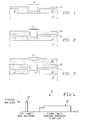
- an integrated circuit device is formed on a semiconductor substrate 10.
- a substrate 10 is described, it will be apparent to those skilled in the art that the described technique may be used with a contact formed to any underlying conductive layer.
- the substrate 10 may include multiple layers of polycrystalline silicon and/or metallic interconnect, as well as being an active region in a monocrystalline silicon substrate.
- An insulating layer 12 is formed over the substrate 10, and an opening 14 formed therethrough as known in the art.
- a barrier layer 16 of titanium nitride is conformally deposited over the insulating layer 12 and in the opening 14. Barrier layer 16 is preferably deposited to a depth of approximately 200 - 500 angstroms.
- an aluminum layer 18 is formed over the barrier layer 16.
- Aluminum layer 18 is preferably formed using known sputtering processes and by keeping the depth and temperature of deposition within certain limits.
- aluminum layer 18 is deposited at a temperature which is as low as possible.
- the purpose of depositing aluminum layer 18 at such a low temperature is to provide an aluminum layer having extremely small grain size. Subsequently deposited aluminum layers will nucleate around the grains formed in layer 18. By minimizing the grain size of aluminum layer 18, the random voiding effect seen in higher temperature, prior art techniques is reduced or eliminated.
- the aluminum layer 18 is an initial layer, and does not form the entire thickness of the interconnect layer.
- the depth to which layer 18 must be deposited will depend on the dimensions of the opening 14. Typical thicknesses of layer 18 will be 500 - 1000 angstroms when opening 14 has a width of between 0.5 and 1 micron.
- Layer 18 is preferably deposited to a depth which insures that a complete layer 18 is deposited. Therefore, layer 18 is typically a nominal thickness of no less than 200 - 300 angstroms.
- the rate at which aluminum layer 18 is deposited is important. In general, the faster the rate of deposition of aluminum layer 18, the better the structure of the resulting layer. Therefore, rates of at least 100 angstroms per second are preferred with rates over 100 angstroms per second producing very good results. However, the technique may be practiced with rates of approximately 50 angstroms per second and below.
- a second aluminum layer 20 is formed over the first aluminum layer 18.
- This layer is formed at lower deposition rates and using techniques which allow the deposited aluminum to completely fill the opening 14.
- the techniques described in detail in U. S. patent 5,108,951, titled METHOD FOR FORMING A METAL CONTACT, issued to Fusen E. Chen et al. are used to form the second aluminum layer 20.
- U.S. Patent 5,108,951 is expressly incorporated by reference. Such techniques provide for a very good inherent step coverage.
- the contact opening 14 is essentially filled by the aluminum layer 20, giving an approximately planar upper surface.
- Deposition of the two layers works together to provide improved contacts. Relatively fast deposition of the first aluminum layer 18 at a low temperature provides for a very small grain size on first aluminum layer 18. Deposition of aluminum layer 18 under these conditions provides poor step coverage. Overall step coverage is improved by deposition of a second aluminum layer 20 under the conditions described in the referenced patent.
- the present method is preferably practiced in conjunction with a multichamber sputtering machine, in which first layer 18 is deposited in a first chamber at room temperature, after which the wafer is moved to a second chamber for deposition of layer 20.
- Heated argon gas typically used to raise the temperature of the wafer during deposition, is not used in the first chamber. However, heated argon gas may be used in the second chamber to raise the temperature of the wafer for deposition of layer 20.
- layer 18 will be deposited in much less time than layer 20. It may be desirable to have several heated chambers allocated for each room temperature chamber used for sputtering of aluminum.
- Figure 4 is a graph 22 illustrating deposition rates of aluminum layers 18, 20 according to one embodiment of the invention.
- curve 24 illustrates that a relatively high deposition rate is used for a short period of time to form layer 18.
- the wafer containing the integrated circuit device is then moved into the second chamber, and layer 20 is deposited according to curve 26 at a lower rate and increasing temperature.
- the temperature and rate of deposition in the second chamber embodies the teachings of the Chen patent incorporated by reference above.
- Curve 26 indicates deposition at a rate of 40 angstroms per second for a short period of time, followed by deposition at 60 angstroms per second.
- Other deposition rates and times such as those described in connection with Figure 4 of the Chen patent, may be used with equally good results.
- the thickness of the first aluminum layer 18 will depend upon the size of the opening 14. The smaller the dimensions of opening 14, the thinner layer 18 must be in order not to completely block the contact opening prior to deposition of layer 20.
- a barrier layer 16 as described in Figure 1 is optional.
- the barrier layer seems to improve the grain sizes of the deposited aluminum layer 18 somewhat. However, even without deposition of barrier layer 16, layer 18 is formed with relatively small grain sizes.
- a barrier layer 16 formed of titanium nitride or other material will generally depend upon the nature of the substrate 10 underlying the opening 14.
- the titanium nitride can be used as a barrier material to prevent aluminum spiking into the substrate 10. If the upper surface of substrate 10 is a polycrystalline silicon interconnect line, or metallic interconnect, the barrier layer 16 may not be necessary.
Landscapes
- Internal Circuitry In Semiconductor Integrated Circuit Devices (AREA)
- Electrodes Of Semiconductors (AREA)
Applications Claiming Priority (2)
| Application Number | Priority Date | Filing Date | Title |
|---|---|---|---|
| US94869092A | 1992-09-22 | 1992-09-22 | |
| US948690 | 1992-09-22 |
Publications (2)
| Publication Number | Publication Date |
|---|---|
| EP0594300A1 true EP0594300A1 (fr) | 1994-04-27 |
| EP0594300B1 EP0594300B1 (fr) | 1998-07-29 |
Family
ID=25488150
Family Applications (1)
| Application Number | Title | Priority Date | Filing Date |
|---|---|---|---|
| EP93307350A Expired - Lifetime EP0594300B1 (fr) | 1992-09-22 | 1993-09-17 | Méthode pour la fabrication d'un contact à métal |
Country Status (4)
| Country | Link |
|---|---|
| US (1) | US5374592A (fr) |
| EP (1) | EP0594300B1 (fr) |
| JP (1) | JPH06216133A (fr) |
| DE (1) | DE69319993T2 (fr) |
Cited By (3)
| Publication number | Priority date | Publication date | Assignee | Title |
|---|---|---|---|---|
| EP0706205A3 (fr) * | 1994-09-19 | 1997-10-22 | Siemens Ag | Procédé de dépÔt planarisant par pulvérisation de couche contenant de l'aluminium dans la fabrication de circuits intégrés |
| EP0877424A3 (fr) * | 1997-04-16 | 1999-09-15 | STMicroelectronics, Inc. | Méthode d'interconnexion et structure pour dispositifs semiconducteurs |
| EP0856885A3 (fr) * | 1997-02-03 | 2000-05-31 | Applied Materials, Inc. | Méthode et dispositif pour réduire "l'effet de première pastille" |
Families Citing this family (20)
| Publication number | Priority date | Publication date | Assignee | Title |
|---|---|---|---|---|
| EP0608628A3 (fr) * | 1992-12-25 | 1995-01-18 | Kawasaki Steel Co | Procédé pour fabriquer un dispositif semi-conducteur ayant une structure d'interconnexion multi-couches. |
| JPH06314744A (ja) * | 1993-04-28 | 1994-11-08 | Fujitsu Ltd | 半導体装置の製造方法 |
| JP3401843B2 (ja) * | 1993-06-21 | 2003-04-28 | ソニー株式会社 | 半導体装置における多層配線の形成方法 |
| US5523259A (en) * | 1994-12-05 | 1996-06-04 | At&T Corp. | Method of forming metal layers formed as a composite of sub-layers using Ti texture control layer |
| KR0179827B1 (ko) * | 1995-05-27 | 1999-04-15 | 문정환 | 반도체 소자의 배선 형성방법 |
| US5851920A (en) * | 1996-01-22 | 1998-12-22 | Motorola, Inc. | Method of fabrication of metallization system |
| US5677238A (en) * | 1996-04-29 | 1997-10-14 | Chartered Semiconductor Manufacturing Pte Ltd | Semiconductor contact metallization |
| US6291336B1 (en) * | 1996-05-20 | 2001-09-18 | Taiwan Semiconductor Manufacturing Company | AlCu metal deposition for robust Rc via performance |
| US6083823A (en) * | 1996-06-28 | 2000-07-04 | International Business Machines Corporation | Metal deposition process for metal lines over topography |
| US5994241A (en) * | 1996-07-31 | 1999-11-30 | International Business Machines Corporation | Method of forming conductive lines on a semiconductor wafer |
| US6309971B1 (en) | 1996-08-01 | 2001-10-30 | Cypress Semiconductor Corporation | Hot metallization process |
| US5798568A (en) * | 1996-08-26 | 1998-08-25 | Motorola, Inc. | Semiconductor component with multi-level interconnect system and method of manufacture |
| US5913146A (en) * | 1997-03-18 | 1999-06-15 | Lucent Technologies Inc. | Semiconductor device having aluminum contacts or vias and method of manufacture therefor |
| EP0867940A3 (fr) | 1997-03-27 | 1999-10-13 | Applied Materials, Inc. | Sous-couche pour interconnexion d'aluminium |
| US5882399A (en) * | 1997-08-23 | 1999-03-16 | Applied Materials, Inc. | Method of forming a barrier layer which enables a consistently highly oriented crystalline structure in a metallic interconnect |
| DE19740330A1 (de) * | 1997-09-13 | 1999-03-25 | Bosch Gmbh Robert | Trägerplatte für Mikrohybridschaltungen |
| US6140228A (en) | 1997-11-13 | 2000-10-31 | Cypress Semiconductor Corporation | Low temperature metallization process |
| US6541371B1 (en) * | 1999-02-08 | 2003-04-01 | Novellus Systems, Inc. | Apparatus and method for depositing superior Ta(N)/copper thin films for barrier and seed applications in semiconductor processing |
| US6420263B1 (en) | 2000-02-28 | 2002-07-16 | International Business Machines Corporation | Method for controlling extrusions in aluminum metal lines and the device formed therefrom |
| US6943105B2 (en) | 2002-01-18 | 2005-09-13 | International Business Machines Corporation | Soft metal conductor and method of making |
Citations (4)
| Publication number | Priority date | Publication date | Assignee | Title |
|---|---|---|---|---|
| US4837183A (en) * | 1988-05-02 | 1989-06-06 | Motorola Inc. | Semiconductor device metallization process |
| EP0488628A2 (fr) * | 1990-11-30 | 1992-06-03 | STMicroelectronics, Inc. | Méthode de fabrication d'un trou de liaison/contact empilées en aluminium pour des interconnexions à multi-couches |
| EP0488264A2 (fr) * | 1990-11-30 | 1992-06-03 | Kabushiki Kaisha Toshiba | Méthode de fabrication d'un dispositif semi-conducteur à résistance contre l'électromigration améliorées |
| EP0499241A1 (fr) * | 1991-02-12 | 1992-08-19 | Applied Materials, Inc. | Procédé de pulvérisation d'une couche d'aluminium sur des plaquettes échelonnées |
Family Cites Families (45)
| Publication number | Priority date | Publication date | Assignee | Title |
|---|---|---|---|---|
| US3158504A (en) * | 1960-10-07 | 1964-11-24 | Texas Instruments Inc | Method of alloying an ohmic contact to a semiconductor |
| US3900598A (en) * | 1972-03-13 | 1975-08-19 | Motorola Inc | Ohmic contacts and method of producing same |
| US4107726A (en) * | 1977-01-03 | 1978-08-15 | Raytheon Company | Multilayer interconnected structure for semiconductor integrated circuit |
| JPS6047739B2 (ja) * | 1977-11-17 | 1985-10-23 | 松下電器産業株式会社 | 半導体装置の製造方法 |
| US4436582A (en) * | 1980-10-28 | 1984-03-13 | Saxena Arjun N | Multilevel metallization process for integrated circuits |
| JPS57139939A (en) * | 1981-02-23 | 1982-08-30 | Seiko Instr & Electronics Ltd | Semiconductor device |
| JPS5846641A (ja) * | 1981-09-14 | 1983-03-18 | Fujitsu Ltd | 半導体装置の製造方法 |
| US4478881A (en) * | 1981-12-28 | 1984-10-23 | Solid State Devices, Inc. | Tungsten barrier contact |
| GB2128636B (en) * | 1982-10-19 | 1986-01-08 | Motorola Ltd | Silicon-aluminium alloy metallization of semiconductor substrate |
| US4495221A (en) * | 1982-10-26 | 1985-01-22 | Signetics Corporation | Variable rate semiconductor deposition process |
| DE3326142A1 (de) * | 1983-07-20 | 1985-01-31 | Siemens AG, 1000 Berlin und 8000 München | Integrierte halbleiterschaltung mit einer aus aluminium oder aus einer aluminiumlegierung bestehenden aeusseren kontaktleiterbahnebene |
| US4502209A (en) * | 1983-08-31 | 1985-03-05 | At&T Bell Laboratories | Forming low-resistance contact to silicon |
| JPS6063926A (ja) * | 1983-08-31 | 1985-04-12 | Fujitsu Ltd | 半導体装置の製造方法 |
| FR2563048B1 (fr) * | 1984-04-13 | 1986-05-30 | Efcis | Procede de realisation de contacts d'aluminium a travers une couche isolante epaisse dans un circuit integre |
| JPS60227446A (ja) * | 1984-04-25 | 1985-11-12 | Mitsubishi Electric Corp | 半導体装置の製造方法 |
| US4566177A (en) * | 1984-05-11 | 1986-01-28 | Signetics Corporation | Formation of electromigration resistant aluminum alloy conductors |
| US4661228A (en) * | 1984-05-17 | 1987-04-28 | Varian Associates, Inc. | Apparatus and method for manufacturing planarized aluminum films |
| JPH069199B2 (ja) * | 1984-07-18 | 1994-02-02 | 株式会社日立製作所 | 配線構造体およびその製造方法 |
| GB2164491B (en) * | 1984-09-14 | 1988-04-07 | Stc Plc | Semiconductor devices |
| JPS61142739A (ja) * | 1984-12-17 | 1986-06-30 | Toshiba Corp | 半導体装置の製造方法 |
| JPH0666155B2 (ja) * | 1985-04-18 | 1994-08-24 | 松下電器産業株式会社 | 電極の形成方法 |
| US4796081A (en) * | 1986-05-02 | 1989-01-03 | Advanced Micro Devices, Inc. | Low resistance metal contact for silicon devices |
| US4759533A (en) * | 1986-08-11 | 1988-07-26 | Dresser Industries, Inc. | Heat-insulating boards |
| US4721689A (en) * | 1986-08-28 | 1988-01-26 | International Business Machines Corporation | Method for simultaneously forming an interconnection level and via studs |
| JPH0691091B2 (ja) * | 1986-11-13 | 1994-11-14 | 富士通株式会社 | 半導体装置の製造方法 |
| JPH081950B2 (ja) * | 1986-11-21 | 1996-01-10 | 株式会社東芝 | 半導体装置の製造方法 |
| JPS63136547A (ja) * | 1986-11-27 | 1988-06-08 | Matsushita Electronics Corp | 半導体装置の配線形成方法 |
| US4756810A (en) * | 1986-12-04 | 1988-07-12 | Machine Technology, Inc. | Deposition and planarizing methods and apparatus |
| JPS63162854A (ja) * | 1986-12-25 | 1988-07-06 | Fujitsu Ltd | 金属膜形成方法 |
| US4782380A (en) * | 1987-01-22 | 1988-11-01 | Advanced Micro Devices, Inc. | Multilayer interconnection for integrated circuit structure having two or more conductive metal layers |
| US4988423A (en) * | 1987-06-19 | 1991-01-29 | Matsushita Electric Industrial Co., Ltd. | Method for fabricating interconnection structure |
| JPS6477122A (en) * | 1987-09-18 | 1989-03-23 | Fujitsu Ltd | Manufacture of semiconductor device |
| JPH0719841B2 (ja) * | 1987-10-02 | 1995-03-06 | 株式会社東芝 | 半導体装置 |
| JPH01160036A (ja) * | 1987-12-17 | 1989-06-22 | Oki Electric Ind Co Ltd | 半導体装置 |
| NL8800359A (nl) * | 1988-02-15 | 1989-09-01 | Philips Nv | Werkwijze voor het vervaardigen van een halfgeleiderinrichting. |
| FR2634317A1 (fr) * | 1988-07-12 | 1990-01-19 | Philips Nv | Procede pour fabriquer un dispositif semiconducteur ayant au moins un niveau de prise de contact a travers des ouvertures de contact de petites dimensions |
| JPH0666287B2 (ja) * | 1988-07-25 | 1994-08-24 | 富士通株式会社 | 半導体装置の製造方法 |
| US4944961A (en) * | 1988-08-05 | 1990-07-31 | Rensselaer Polytechnic Institute | Deposition of metals on stepped surfaces |
| JPH02137230A (ja) * | 1988-11-17 | 1990-05-25 | Nec Corp | 集積回路装置 |
| US4994162A (en) * | 1989-09-29 | 1991-02-19 | Materials Research Corporation | Planarization method |
| US4970176A (en) * | 1989-09-29 | 1990-11-13 | Motorola, Inc. | Multiple step metallization process |
| US4975389A (en) * | 1989-10-25 | 1990-12-04 | At&T Bell Laboratories | Aluminum metallization for semiconductor devices |
| DE69031903T2 (de) * | 1989-11-30 | 1998-04-16 | Sgs Thomson Microelectronics | Verfahren zum Herstellen von Zwischenschicht-Kontakten |
| US5108951A (en) * | 1990-11-05 | 1992-04-28 | Sgs-Thomson Microelectronics, Inc. | Method for forming a metal contact |
| US5108570A (en) * | 1990-03-30 | 1992-04-28 | Applied Materials, Inc. | Multistep sputtering process for forming aluminum layer over stepped semiconductor wafer |
-
1993
- 1993-09-17 EP EP93307350A patent/EP0594300B1/fr not_active Expired - Lifetime
- 1993-09-17 DE DE69319993T patent/DE69319993T2/de not_active Expired - Fee Related
- 1993-09-22 JP JP5236089A patent/JPH06216133A/ja active Pending
-
1994
- 1994-02-07 US US08/192,786 patent/US5374592A/en not_active Expired - Lifetime
Patent Citations (4)
| Publication number | Priority date | Publication date | Assignee | Title |
|---|---|---|---|---|
| US4837183A (en) * | 1988-05-02 | 1989-06-06 | Motorola Inc. | Semiconductor device metallization process |
| EP0488628A2 (fr) * | 1990-11-30 | 1992-06-03 | STMicroelectronics, Inc. | Méthode de fabrication d'un trou de liaison/contact empilées en aluminium pour des interconnexions à multi-couches |
| EP0488264A2 (fr) * | 1990-11-30 | 1992-06-03 | Kabushiki Kaisha Toshiba | Méthode de fabrication d'un dispositif semi-conducteur à résistance contre l'électromigration améliorées |
| EP0499241A1 (fr) * | 1991-02-12 | 1992-08-19 | Applied Materials, Inc. | Procédé de pulvérisation d'une couche d'aluminium sur des plaquettes échelonnées |
Cited By (4)
| Publication number | Priority date | Publication date | Assignee | Title |
|---|---|---|---|---|
| EP0706205A3 (fr) * | 1994-09-19 | 1997-10-22 | Siemens Ag | Procédé de dépÔt planarisant par pulvérisation de couche contenant de l'aluminium dans la fabrication de circuits intégrés |
| EP0856885A3 (fr) * | 1997-02-03 | 2000-05-31 | Applied Materials, Inc. | Méthode et dispositif pour réduire "l'effet de première pastille" |
| US6139698A (en) * | 1997-02-03 | 2000-10-31 | Applied Materials, Inc. | Method and apparatus for reducing the first wafer effect |
| EP0877424A3 (fr) * | 1997-04-16 | 1999-09-15 | STMicroelectronics, Inc. | Méthode d'interconnexion et structure pour dispositifs semiconducteurs |
Also Published As
| Publication number | Publication date |
|---|---|
| EP0594300B1 (fr) | 1998-07-29 |
| US5374592A (en) | 1994-12-20 |
| DE69319993D1 (de) | 1998-09-03 |
| DE69319993T2 (de) | 1998-12-10 |
| JPH06216133A (ja) | 1994-08-05 |
Similar Documents
| Publication | Publication Date | Title |
|---|---|---|
| US5374592A (en) | Method for forming an aluminum metal contact | |
| EP0485130B1 (fr) | Procédé pour former un contact métallique | |
| EP0655780B1 (fr) | Procédé de fabrication d'un contact en aluminium | |
| US5472912A (en) | Method of making an integrated circuit structure by using a non-conductive plug | |
| US5523259A (en) | Method of forming metal layers formed as a composite of sub-layers using Ti texture control layer | |
| US5918149A (en) | Deposition of a conductor in a via hole or trench | |
| US5580823A (en) | Process for fabricating a collimated metal layer and contact structure in a semiconductor device | |
| US5668055A (en) | Method of filling of contact openings and vias by self-extrusion of overlying compressively stressed matal layer | |
| US5318923A (en) | Method for forming a metal wiring layer in a semiconductor device | |
| EP0558304B1 (fr) | Procédé de fabrication de contacts submicroniques | |
| EP0488628B1 (fr) | Méthode de fabrication d'un trou de liaison/contact empilées en aluminium pour des interconnexions à multi-couches | |
| US6215188B1 (en) | Low temperature aluminum reflow for multilevel metallization | |
| EP0583876B1 (fr) | Contact planaire comportant un vide | |
| US6093968A (en) | Germanium alloy contact to a silicon substrate | |
| US6271137B1 (en) | Method of producing an aluminum stacked contact/via for multilayer | |
| US6287963B1 (en) | Method for forming a metal contact | |
| US6979642B1 (en) | Method of self-annealing conductive lines that separates grain size effects from alloy mobility | |
| EP0552893B1 (fr) | Procédé de fabrication d'un contact en aluminium | |
| US6518185B1 (en) | Integration scheme for non-feature-size dependent cu-alloy introduction |
Legal Events
| Date | Code | Title | Description |
|---|---|---|---|
| PUAI | Public reference made under article 153(3) epc to a published international application that has entered the european phase |
Free format text: ORIGINAL CODE: 0009012 |
|
| AK | Designated contracting states |
Kind code of ref document: A1 Designated state(s): DE FR GB IT |
|
| 17P | Request for examination filed |
Effective date: 19941024 |
|
| 17Q | First examination report despatched |
Effective date: 19941122 |
|
| GRAG | Despatch of communication of intention to grant |
Free format text: ORIGINAL CODE: EPIDOS AGRA |
|
| RHK1 | Main classification (correction) |
Ipc: H01L 21/285 |
|
| GRAG | Despatch of communication of intention to grant |
Free format text: ORIGINAL CODE: EPIDOS AGRA |
|
| GRAH | Despatch of communication of intention to grant a patent |
Free format text: ORIGINAL CODE: EPIDOS IGRA |
|
| GRAH | Despatch of communication of intention to grant a patent |
Free format text: ORIGINAL CODE: EPIDOS IGRA |
|
| GRAA | (expected) grant |
Free format text: ORIGINAL CODE: 0009210 |
|
| AK | Designated contracting states |
Kind code of ref document: B1 Designated state(s): DE FR GB IT |
|
| REF | Corresponds to: |
Ref document number: 69319993 Country of ref document: DE Date of ref document: 19980903 |
|
| ET | Fr: translation filed | ||
| RAP4 | Party data changed (patent owner data changed or rights of a patent transferred) |
Owner name: STMICROELECTRONICS, INC. |
|
| PLBE | No opposition filed within time limit |
Free format text: ORIGINAL CODE: 0009261 |
|
| STAA | Information on the status of an ep patent application or granted ep patent |
Free format text: STATUS: NO OPPOSITION FILED WITHIN TIME LIMIT |
|
| 26N | No opposition filed | ||
| PGFP | Annual fee paid to national office [announced via postgrant information from national office to epo] |
Ref country code: DE Payment date: 19990927 Year of fee payment: 7 |
|
| PG25 | Lapsed in a contracting state [announced via postgrant information from national office to epo] |
Ref country code: DE Free format text: LAPSE BECAUSE OF NON-PAYMENT OF DUE FEES Effective date: 20010601 |
|
| REG | Reference to a national code |
Ref country code: GB Ref legal event code: IF02 |
|
| PGFP | Annual fee paid to national office [announced via postgrant information from national office to epo] |
Ref country code: FR Payment date: 20030909 Year of fee payment: 11 |
|
| PGFP | Annual fee paid to national office [announced via postgrant information from national office to epo] |
Ref country code: GB Payment date: 20030917 Year of fee payment: 11 |
|
| PG25 | Lapsed in a contracting state [announced via postgrant information from national office to epo] |
Ref country code: GB Free format text: LAPSE BECAUSE OF NON-PAYMENT OF DUE FEES Effective date: 20040917 |
|
| GBPC | Gb: european patent ceased through non-payment of renewal fee |
Effective date: 20040917 |
|
| PG25 | Lapsed in a contracting state [announced via postgrant information from national office to epo] |
Ref country code: FR Free format text: LAPSE BECAUSE OF NON-PAYMENT OF DUE FEES Effective date: 20050531 |
|
| REG | Reference to a national code |
Ref country code: FR Ref legal event code: ST |
|
| PG25 | Lapsed in a contracting state [announced via postgrant information from national office to epo] |
Ref country code: IT Free format text: LAPSE BECAUSE OF NON-PAYMENT OF DUE FEES;WARNING: LAPSES OF ITALIAN PATENTS WITH EFFECTIVE DATE BEFORE 2007 MAY HAVE OCCURRED AT ANY TIME BEFORE 2007. THE CORRECT EFFECTIVE DATE MAY BE DIFFERENT FROM THE ONE RECORDED. Effective date: 20050917 |