EP0594473B1 - Mikrokontroller verfügend über einen Emulationsmodus mit internen und externen Peripherie - Google Patents
Mikrokontroller verfügend über einen Emulationsmodus mit internen und externen Peripherie Download PDFInfo
- Publication number
- EP0594473B1 EP0594473B1 EP93402376A EP93402376A EP0594473B1 EP 0594473 B1 EP0594473 B1 EP 0594473B1 EP 93402376 A EP93402376 A EP 93402376A EP 93402376 A EP93402376 A EP 93402376A EP 0594473 B1 EP0594473 B1 EP 0594473B1
- Authority
- EP
- European Patent Office
- Prior art keywords
- external
- internal
- input
- central processor
- signal
- Prior art date
- Legal status (The legal status is an assumption and is not a legal conclusion. Google has not performed a legal analysis and makes no representation as to the accuracy of the status listed.)
- Expired - Lifetime
Links
Images
Classifications
-
- G—PHYSICS
- G06—COMPUTING OR CALCULATING; COUNTING
- G06F—ELECTRIC DIGITAL DATA PROCESSING
- G06F11/00—Error detection; Error correction; Monitoring
- G06F11/36—Prevention of errors by analysis, debugging or testing of software
- G06F11/362—Debugging of software
- G06F11/3648—Debugging of software using additional hardware
-
- G—PHYSICS
- G06—COMPUTING OR CALCULATING; COUNTING
- G06F—ELECTRIC DIGITAL DATA PROCESSING
- G06F11/00—Error detection; Error correction; Monitoring
- G06F11/22—Detection or location of defective computer hardware by testing during standby operation or during idle time, e.g. start-up testing
- G06F11/26—Functional testing
- G06F11/261—Functional testing by simulating additional hardware, e.g. fault simulation
-
- G—PHYSICS
- G06—COMPUTING OR CALCULATING; COUNTING
- G06F—ELECTRIC DIGITAL DATA PROCESSING
- G06F13/00—Interconnection of, or transfer of information or other signals between, memories, input/output devices or central processing units
- G06F13/38—Information transfer, e.g. on bus
- G06F13/42—Bus transfer protocol, e.g. handshake; Synchronisation
- G06F13/4204—Bus transfer protocol, e.g. handshake; Synchronisation on a parallel bus
- G06F13/4208—Bus transfer protocol, e.g. handshake; Synchronisation on a parallel bus being a system bus, e.g. VME bus, Futurebus, Multibus
Definitions
- the present invention relates to a microcomputer capable of operating in emulation mode with external and internal peripherals.
- a microcomputer generally comprises a central processor called CPU ("Central Processing Unit"), at least one internal peripheral (clock, analog to digital converter, etc.), an internal address decoder and an internal memory (ROM, RAM, EEPROM, EPROM, ...), connected by a data and address bus.
- the central processor has ports and a connection bus to the outside in user mode.
- the object of the present invention is to obviate this drawback, by means of a microcomputer having internal peripherals and external peripherals which are selectively accessible.
- a microcomputer having internal peripherals and external peripherals which are selectively accessible.
- the ports of the microcomputer are connected to external devices and to an external address decoder.
- the external address decoder transmits a signal applied to the central processor to block the preloading of the internal address decoder when an external device is selected.
- external memories are also connected to the input / output ports, an external device having access only to an external memory.
- the central processor comprises at least one interrupt input usable by a peripheral
- the interrupt request signals coming from the internal and external peripherals are respectively applied in emulation mode to the inputs of an OR gate whose output is connected to the interrupt input of the central processor.
- the interrupt signal from the external device is first applied to an input of a door AND to the other input of which is applied a signal corresponding to the operating mode of the microcomputer.
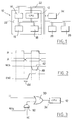
- a microcomputer 10 comprises a central processor 12, peripherals 16, memories 18 and an internal address decoder 14, these various components being connected to a data and address bus 20
- the central processor 12 has input / output ports 22 to the outside in user mode.
- the external peripherals 28 and external memories 26 are connected to the input / output ports of the central processor 12.
- the input / output ports to the exterior of the central computer 12 are used in data bus, and in address and control bus.
- an external address decoder 24 is connected to the input / output ports to the outside of the central processor 12. This decoder returns a signal indicating whether the address of a peripheral is an internal address or external.
- the exchange of information between the peripherals 16 and the central processor 12 takes place by means of signals comprising, as shown in FIG. 2 succinctly, a clock signal H of the square slot type, sixteen address signals A positioned on the falling edges of the clock signal, eight data signals, not shown in FIG. 2, the values of which change during the rising edges of the clock signal, a signal also not shown indicating whether it is a write or read, a device selection signal generated by the address decoder, and finally an interrupt signal from the central processor.
- signals comprising, as shown in FIG. 2 succinctly, a clock signal H of the square slot type, sixteen address signals A positioned on the falling edges of the clock signal, eight data signals, not shown in FIG. 2, the values of which change during the rising edges of the clock signal, a signal also not shown indicating whether it is a write or read, a device selection signal generated by the address decoder, and finally an interrupt signal from the central processor.
- the device selection signal shown under the initials NCS in Figure 2 is normally active at the low state.
- the clock signal is low, there is preload of the address decoder.
- the selection signals are activated and the selection signal goes low (40, Figure 2).
- the addressing of a peripheral by the central processor 12 is done in a clock cycle H as follows: when the clock signal is in the low state, there is positioning of the addresses by the central processor 12, positioning of the write / read signal, and preloading of the address decoder. When the clock signal goes high, the preloading of the address decoder ceases and there is activation of the selection signal of the selected device, then the data is forced on the data bus by the central processor 12 during a write cycle or by the device chosen when there is a read cycle. Obviously, an interrupt request to the central processor can be made at any time by a peripheral.
- an external address decoder 24 is connected to the input / output ports 22, as well as peripherals 28 and memories 26.
- the external address decoder 24 transmits a signal (CSI, figure 2) changing state depending on the address indicated, i.e. remaining low as long as the address indicated is an internal address and passing to high state when the address indicated is an address external to microcomputer 10. This signal is reintroduced into the central processor 12.
- addressing makes it possible to choose an internal or external address.
- the addressing of the peripherals by the central processor 12 is also done in a clock cycle H.
- the clock When the clock is in the low state, there is positioning of the addresses by the central processor 12, positioning of the read / write signal, preloading of the internal address decoder but there is in addition the external decoding of the addresses by the decoder 24 and emission of the CSI signal resulting from external decoding.
- the clock signal H goes high, there are two possibilities depending on the state of the CSI signal. If the CSI signal is in a low state, this means that an internal peripheral 16 has been selected, and the microcomputer 10 acts as usual.
- the signal NCS of preload of the internal address decoder remains blocked in the high state as indicated by dashes 42 FIG. 2 and there is then forcing of the data on the input / output ports 22 then operating in data bus either by the central processor 12 on a write cycle, or by the external device 28 on a read cycle.
- the signal CSI generated by the external address decoder 24 changes state only while the clock signal H is in the low state.
- This offset 44 is less than the half clock cycle and this fact does not prevent the blocking of the preload signal from the required internal address decoder.
- FIG. 3 shows one of the interrupt inputs of the central processor 12. This interrupt input 34 is connected to the output of an OR gate 30 to the two inputs to which the interrupt request signals are applied.
- One of these two OR gate 30 inputs directly receives the internal interrupt request signal II and the other input receives an interrupt request signal from an external IE device via a gate AND allowing the request to be validated if the microcomputer is operating in emulation mode.
- a signal corresponding to the U / E mode used that is to say to the user mode or emulation mode, is applied to the other input gate of the AND gate 32.
Landscapes
- Engineering & Computer Science (AREA)
- Theoretical Computer Science (AREA)
- Computer Hardware Design (AREA)
- General Engineering & Computer Science (AREA)
- Physics & Mathematics (AREA)
- General Physics & Mathematics (AREA)
- Quality & Reliability (AREA)
- Test And Diagnosis Of Digital Computers (AREA)
- Microcomputers (AREA)
Claims (3)
- Mikrokontroller, der mit äußerer Peripherie in einer Emulationsbetriebsart arbeiten kann, umfassend einen zentralen Prozessor (12), zumindest eine innere Peripherie (16), einen inneren Adreßdekodierer (14) und einen inneren Speicher (18), die über einen Adreß- und Datenbus (20) verbunden sind, wobei der zentrale Prozessor (12) in der Anwenderbetriebsart Eingangs-/Ausgangsports (22) nach außen hin umfaßt, dadurch gekennzeichnet, daß die Eingangs-/Ausgangsports (22) in der Emulationsbetriebsart mit der äußeren Peripherie (28) bzw. einem äußeren Adreßdekodierer (24) verbunden sind, wobei der äußere Adreßdekodierer (24) ein Signal ausgibt, welches dem zentralen Prozessor zugeführt wird, um die Vorladung des inneren Adreßdekodierers (14) zu sperren, wenn eine äußere Peripherie (28) ausgewählt ist.
- Mikrokontroller nach Anspruch 1, dadurch gekennzeichnet, daß gleichfalls äußere Speicher (26) mit den Eingangs-/Ausgangsports verbunden sind.
- Mikrokontroller nach einem der Ansprüche 1 oder 2, bei dem der zentrale Prozessor (12) zumindest einen Unterbrechungseingang umfaßt, dadurch gekennzeichnet, daß die von der inneren (16) und äußeren (28) Peripherie stammenden Unterbrechungs-Anforderungssignale jeweils den Eingängen eines ODER-Tors (30) zugeführt werden, dessen Ausgang mit dem genannten Unterbrechungseingang (34) verbunden ist, wobei das von einer äußeren Peripherie (28) stammende Unterbrechungs-Anforderungssignal zuvor dem Eingang eines UND-Tors (32) zugeführt wird, dessen anderem Eingang ein der Betriebsart des Mikrokontrollers (10) entsprechendes Signal zugeführt wird.
Applications Claiming Priority (2)
| Application Number | Priority Date | Filing Date | Title |
|---|---|---|---|
| FR9211716 | 1992-10-02 | ||
| FR9211716A FR2696561B1 (fr) | 1992-10-02 | 1992-10-02 | Micro-calculateur pouvant fonctionner en mode d'émulation avec des périphériques internes et externes. |
Publications (2)
| Publication Number | Publication Date |
|---|---|
| EP0594473A1 EP0594473A1 (de) | 1994-04-27 |
| EP0594473B1 true EP0594473B1 (de) | 1995-04-12 |
Family
ID=9434096
Family Applications (1)
| Application Number | Title | Priority Date | Filing Date |
|---|---|---|---|
| EP93402376A Expired - Lifetime EP0594473B1 (de) | 1992-10-02 | 1993-09-29 | Mikrokontroller verfügend über einen Emulationsmodus mit internen und externen Peripherie |
Country Status (5)
| Country | Link |
|---|---|
| US (1) | US5692161A (de) |
| EP (1) | EP0594473B1 (de) |
| JP (1) | JP3452147B2 (de) |
| DE (1) | DE69300109T2 (de) |
| FR (1) | FR2696561B1 (de) |
Families Citing this family (6)
| Publication number | Priority date | Publication date | Assignee | Title |
|---|---|---|---|---|
| JPH0728665A (ja) * | 1993-07-07 | 1995-01-31 | Nec Corp | マイクロコンピュータ用エミュレーション装置 |
| JP2793540B2 (ja) * | 1995-12-27 | 1998-09-03 | 日本電気アイシーマイコンシステム株式会社 | エミュレーション装置 |
| DE59908019D1 (de) * | 1998-09-02 | 2004-01-22 | Infineon Technologies Ag | Verfahren und vorrichtung zur systemsimulation von mikrocontrollern/mikroprozessoren und zugehörenden peripheriemodulen |
| US6571360B1 (en) * | 1999-10-19 | 2003-05-27 | Sun Microsystems, Inc. | Cage for dynamic attach testing of I/O boards |
| CN101354730B (zh) * | 2005-08-31 | 2010-08-25 | 上海海尔集成电路有限公司 | 一种仿真器芯片的仿真方法 |
| CN100357909C (zh) * | 2005-08-31 | 2007-12-26 | 上海海尔集成电路有限公司 | 一种仿真器芯片 |
Family Cites Families (17)
| Publication number | Priority date | Publication date | Assignee | Title |
|---|---|---|---|---|
| US4441154A (en) * | 1981-04-13 | 1984-04-03 | Texas Instruments Incorporated | Self-emulator microcomputer |
| US4797808A (en) * | 1981-06-22 | 1989-01-10 | Texas Instruments Incorporated | Microcomputer with self-test of macrocode |
| US4514805A (en) * | 1982-02-22 | 1985-04-30 | Texas Instruments Incorporated | Interrupt operation in systems emulator mode for microcomputer |
| US4649471A (en) * | 1983-03-01 | 1987-03-10 | Thomson Components-Mostek Corporation | Address-controlled automatic bus arbitration and address modification |
| US5140687A (en) * | 1985-10-22 | 1992-08-18 | Texas Instruments Incorporated | Data processing apparatus with self-emulation capability |
| US4875186A (en) * | 1986-02-28 | 1989-10-17 | Prime Computer, Inc. | Peripheral emulation apparatus |
| US5001624A (en) * | 1987-02-13 | 1991-03-19 | Harrell Hoffman | Processor controlled DMA controller for transferring instruction and data from memory to coprocessor |
| US5155812A (en) * | 1989-05-04 | 1992-10-13 | Texas Instruments Incorporated | Devices and method for generating and using systems, software waitstates on address boundaries in data processing |
| JPH0679307B2 (ja) * | 1987-10-22 | 1994-10-05 | 日本電気株式会社 | コプロセッサの並行動作制御方式 |
| US5084814A (en) * | 1987-10-30 | 1992-01-28 | Motorola, Inc. | Data processor with development support features |
| JPH0724029B2 (ja) * | 1988-04-13 | 1995-03-15 | 日本電気株式会社 | エミュレーション装置 |
| US5053949A (en) * | 1989-04-03 | 1991-10-01 | Motorola, Inc. | No-chip debug peripheral which uses externally provided instructions to control a core processing unit |
| US5155839A (en) * | 1989-09-29 | 1992-10-13 | Allen-Bradley Company, Inc. | Apparatus using in undifferentiated strobe output to interface either of two incompatible memory access signal types to a memory |
| JPH03204737A (ja) * | 1990-01-08 | 1991-09-06 | Nec Corp | 信号処理プロセッサのデバッグ回路 |
| US5247642A (en) * | 1990-12-05 | 1993-09-21 | Ast Research, Inc. | Apparatus for determining cacheability of a memory address to provide zero wait state operation in a computer system |
| US5291584A (en) * | 1991-07-23 | 1994-03-01 | Nexcom Technology, Inc. | Methods and apparatus for hard disk emulation |
| US5457802A (en) * | 1993-05-17 | 1995-10-10 | Motorola, Inc. | Integrated circuit pin control apparatus and method thereof in a data processing system |
-
1992
- 1992-10-02 FR FR9211716A patent/FR2696561B1/fr not_active Expired - Fee Related
-
1993
- 1993-09-29 DE DE69300109T patent/DE69300109T2/de not_active Expired - Fee Related
- 1993-09-29 EP EP93402376A patent/EP0594473B1/de not_active Expired - Lifetime
- 1993-10-04 JP JP27131293A patent/JP3452147B2/ja not_active Expired - Fee Related
-
1995
- 1995-07-31 US US08/509,218 patent/US5692161A/en not_active Expired - Lifetime
Also Published As
| Publication number | Publication date |
|---|---|
| DE69300109T2 (de) | 1995-08-17 |
| DE69300109D1 (de) | 1995-05-18 |
| JPH06236291A (ja) | 1994-08-23 |
| US5692161A (en) | 1997-11-25 |
| FR2696561A1 (fr) | 1994-04-08 |
| EP0594473A1 (de) | 1994-04-27 |
| FR2696561B1 (fr) | 1994-12-23 |
| JP3452147B2 (ja) | 2003-09-29 |
Similar Documents
| Publication | Publication Date | Title |
|---|---|---|
| FR2862147A1 (fr) | Reconfiguration dynamique de liaisons de type pci-express | |
| FR2539239A1 (fr) | Systeme d'ordinateur a taches multiples a gestion de memoire | |
| EP0594473B1 (de) | Mikrokontroller verfügend über einen Emulationsmodus mit internen und externen Peripherie | |
| FR2776788A1 (fr) | Procede de commutation d'applications sur une carte a puce multi-applicative | |
| EP0186248B1 (de) | Fernsteuerempfänger unter Anwendung einer modulierten Trägerwelle | |
| FR2479534A1 (fr) | Circuit de detection d'erreur pour une memoire | |
| FR2575305A1 (fr) | Dispositif de commande par touches | |
| BE1000154A6 (fr) | Unite d'extension de bus a grande vitesse. | |
| EP0459863B1 (de) | Integrierter Schaltkreis mit Anschlussstift zur Modusfeststellung | |
| FR2765706A1 (fr) | Lecteur de cartes a puces a protocole de transmission rapide | |
| FR2632092A1 (fr) | Circuit de conditionnement d'ecriture d'antememoire retarde pour un systeme de microcalculateur a bus double comprenant une unite 80386 et une unite 82385 | |
| FR2570524A1 (fr) | Terminal de tele-informatique a extensions externes | |
| EP1865412B1 (de) | Steuerung einer Multifunktionsvorrichtung | |
| FR2744539A1 (fr) | Systeme et procede de traitement par augmentation du nombre d'entrees de donnees | |
| FR2884629A1 (fr) | Dispositif d'amelioration de la bande passante pour des circuits munis de controleurs memoires multiples | |
| FR2596890A1 (fr) | Systeme de traitement de l'information avec comparaison anticipee de la programmation | |
| EP0700194A1 (de) | Telefoneinrichtung zur Benutzung mehrerer Speicherkarten | |
| EP0575228B1 (de) | Verfahren zum Laden eines Programms in einen Programmspeicher eines Prozessors | |
| FR2779542A1 (fr) | Circuit integre comportant au moins deux memoires | |
| FR2774836A1 (fr) | Dispositif de transmission bi-directionnelle | |
| EP0138709B1 (de) | Prüfung des Ladens von zum Serienparalleltyp gehörenden integrierten Schaltungen, mit von den Ausgabestufen getrenntem Laderegister | |
| EP0768674A1 (de) | Initialisierungsprozess eines Schieberegisters und dazugehöriges Register | |
| EP0441707B1 (de) | Koppler für Serienbus | |
| EP1233402A1 (de) | Gerät zur Verarbeitung graphischer Muster mit unterschiedlichen Formaten durch Pixelextraktion und Leitweglenkung zu unterschiedlichen Kodiermitteln | |
| FR2841680A1 (fr) | Dispositif de stockage de donnees multiports, en particulier pour une unte arithmetique et logique d'un processeur de traitement numerique du signal |
Legal Events
| Date | Code | Title | Description |
|---|---|---|---|
| PUAI | Public reference made under article 153(3) epc to a published international application that has entered the european phase |
Free format text: ORIGINAL CODE: 0009012 |
|
| AK | Designated contracting states |
Kind code of ref document: A1 Designated state(s): DE FR GB IT |
|
| 17P | Request for examination filed |
Effective date: 19940518 |
|
| 17Q | First examination report despatched |
Effective date: 19940822 |
|
| GRAA | (expected) grant |
Free format text: ORIGINAL CODE: 0009210 |
|
| AK | Designated contracting states |
Kind code of ref document: B1 Designated state(s): DE FR GB IT |
|
| REF | Corresponds to: |
Ref document number: 69300109 Country of ref document: DE Date of ref document: 19950518 |
|
| ITF | It: translation for a ep patent filed | ||
| GBT | Gb: translation of ep patent filed (gb section 77(6)(a)/1977) |
Effective date: 19950425 |
|
| PLBE | No opposition filed within time limit |
Free format text: ORIGINAL CODE: 0009261 |
|
| STAA | Information on the status of an ep patent application or granted ep patent |
Free format text: STATUS: NO OPPOSITION FILED WITHIN TIME LIMIT |
|
| 26N | No opposition filed | ||
| REG | Reference to a national code |
Ref country code: GB Ref legal event code: IF02 |
|
| PGFP | Annual fee paid to national office [announced via postgrant information from national office to epo] |
Ref country code: DE Payment date: 20021002 Year of fee payment: 10 |
|
| PG25 | Lapsed in a contracting state [announced via postgrant information from national office to epo] |
Ref country code: DE Free format text: LAPSE BECAUSE OF NON-PAYMENT OF DUE FEES Effective date: 20040401 |
|
| PGFP | Annual fee paid to national office [announced via postgrant information from national office to epo] |
Ref country code: FR Payment date: 20040908 Year of fee payment: 12 |
|
| PGFP | Annual fee paid to national office [announced via postgrant information from national office to epo] |
Ref country code: GB Payment date: 20040929 Year of fee payment: 12 |
|
| PG25 | Lapsed in a contracting state [announced via postgrant information from national office to epo] |
Ref country code: IT Free format text: LAPSE BECAUSE OF NON-PAYMENT OF DUE FEES;WARNING: LAPSES OF ITALIAN PATENTS WITH EFFECTIVE DATE BEFORE 2007 MAY HAVE OCCURRED AT ANY TIME BEFORE 2007. THE CORRECT EFFECTIVE DATE MAY BE DIFFERENT FROM THE ONE RECORDED. Effective date: 20050929 Ref country code: GB Free format text: LAPSE BECAUSE OF NON-PAYMENT OF DUE FEES Effective date: 20050929 |
|
| GBPC | Gb: european patent ceased through non-payment of renewal fee |
Effective date: 20050929 |
|
| PG25 | Lapsed in a contracting state [announced via postgrant information from national office to epo] |
Ref country code: FR Free format text: LAPSE BECAUSE OF NON-PAYMENT OF DUE FEES Effective date: 20060531 |
|
| REG | Reference to a national code |
Ref country code: FR Ref legal event code: ST Effective date: 20060531 |