EP0596522A1 - Hochfrequenter Kristallresonator - Google Patents
Hochfrequenter Kristallresonator Download PDFInfo
- Publication number
- EP0596522A1 EP0596522A1 EP93117977A EP93117977A EP0596522A1 EP 0596522 A1 EP0596522 A1 EP 0596522A1 EP 93117977 A EP93117977 A EP 93117977A EP 93117977 A EP93117977 A EP 93117977A EP 0596522 A1 EP0596522 A1 EP 0596522A1
- Authority
- EP
- European Patent Office
- Prior art keywords
- resonating
- support structure
- wafer
- membrane
- combination
- Prior art date
- Legal status (The legal status is an assumption and is not a legal conclusion. Google has not performed a legal analysis and makes no representation as to the accuracy of the status listed.)
- Withdrawn
Links
- 239000013078 crystal Substances 0.000 title claims description 56
- 239000012528 membrane Substances 0.000 claims abstract description 51
- VYPSYNLAJGMNEJ-UHFFFAOYSA-N silicon dioxide Inorganic materials O=[Si]=O VYPSYNLAJGMNEJ-UHFFFAOYSA-N 0.000 claims abstract description 19
- 239000010453 quartz Substances 0.000 claims abstract description 18
- 239000010931 gold Substances 0.000 claims description 14
- 229910052737 gold Inorganic materials 0.000 claims description 14
- PCHJSUWPFVWCPO-UHFFFAOYSA-N gold Chemical compound [Au] PCHJSUWPFVWCPO-UHFFFAOYSA-N 0.000 claims description 13
- 230000008878 coupling Effects 0.000 claims description 10
- 238000010168 coupling process Methods 0.000 claims description 10
- 238000005859 coupling reaction Methods 0.000 claims description 10
- 229910052751 metal Inorganic materials 0.000 claims description 6
- 239000002184 metal Substances 0.000 claims description 6
- VYZAMTAEIAYCRO-UHFFFAOYSA-N Chromium Chemical compound [Cr] VYZAMTAEIAYCRO-UHFFFAOYSA-N 0.000 claims description 5
- 229910052782 aluminium Inorganic materials 0.000 claims description 5
- XAGFODPZIPBFFR-UHFFFAOYSA-N aluminium Chemical compound [Al] XAGFODPZIPBFFR-UHFFFAOYSA-N 0.000 claims description 5
- 238000003486 chemical etching Methods 0.000 claims description 5
- 229910052804 chromium Inorganic materials 0.000 claims description 5
- 239000011651 chromium Substances 0.000 claims description 5
- 238000005304 joining Methods 0.000 claims description 5
- 238000005530 etching Methods 0.000 claims description 4
- 239000000463 material Substances 0.000 claims description 2
- 238000004519 manufacturing process Methods 0.000 abstract description 3
- 239000004065 semiconductor Substances 0.000 abstract 1
- 235000012431 wafers Nutrition 0.000 description 16
- 238000000034 method Methods 0.000 description 10
- 238000001465 metallisation Methods 0.000 description 6
- 230000008569 process Effects 0.000 description 4
- 230000001154 acute effect Effects 0.000 description 3
- 230000008901 benefit Effects 0.000 description 3
- RZVXOCDCIIFGGH-UHFFFAOYSA-N chromium gold Chemical class [Cr].[Au] RZVXOCDCIIFGGH-UHFFFAOYSA-N 0.000 description 2
- 238000000227 grinding Methods 0.000 description 2
- 230000000873 masking effect Effects 0.000 description 2
- 150000002739 metals Chemical class 0.000 description 2
- 238000012986 modification Methods 0.000 description 2
- 230000004048 modification Effects 0.000 description 2
- 230000010355 oscillation Effects 0.000 description 2
- 230000001360 synchronised effect Effects 0.000 description 2
- 239000004593 Epoxy Substances 0.000 description 1
- 239000011248 coating agent Substances 0.000 description 1
- 238000000576 coating method Methods 0.000 description 1
- 239000004020 conductor Substances 0.000 description 1
- 238000011109 contamination Methods 0.000 description 1
- 238000005520 cutting process Methods 0.000 description 1
- 238000013016 damping Methods 0.000 description 1
- 230000001419 dependent effect Effects 0.000 description 1
- 238000010586 diagram Methods 0.000 description 1
- 230000000694 effects Effects 0.000 description 1
- 230000002349 favourable effect Effects 0.000 description 1
- 239000011521 glass Substances 0.000 description 1
- 150000002343 gold Chemical class 0.000 description 1
- 230000001788 irregular Effects 0.000 description 1
- 239000007788 liquid Substances 0.000 description 1
- 238000005259 measurement Methods 0.000 description 1
- 238000007747 plating Methods 0.000 description 1
- 238000005498 polishing Methods 0.000 description 1
- 239000000523 sample Substances 0.000 description 1
- 238000005070 sampling Methods 0.000 description 1
- 229920006395 saturated elastomer Polymers 0.000 description 1
- 238000007789 sealing Methods 0.000 description 1
- 238000007493 shaping process Methods 0.000 description 1
- 239000000126 substance Substances 0.000 description 1
- 230000007704 transition Effects 0.000 description 1
Images


Classifications
-
- H—ELECTRICITY
- H03—ELECTRONIC CIRCUITRY
- H03H—IMPEDANCE NETWORKS, e.g. RESONANT CIRCUITS; RESONATORS
- H03H9/00—Networks comprising electromechanical or electro-acoustic elements; Electromechanical resonators
- H03H9/15—Constructional features of resonators consisting of piezoelectric or electrostrictive material
- H03H9/17—Constructional features of resonators consisting of piezoelectric or electrostrictive material having a single resonator
- H03H9/19—Constructional features of resonators consisting of piezoelectric or electrostrictive material having a single resonator consisting of quartz
Definitions
- This invention relates to crystal resonators and, more particularly, to a high frequency crystal resonator with a resonating frequency on the order of 30 MHz or greater.
- Crystal resonators are used in a variety of timing dependent applications, such as in computers.
- Computers are capable of executing multiple tasks simultaneously. Yet such execution typically involves sharing buses, memory, and other common structures. Computers are therefore synchronized to a high frequency clock signal to maintain data integrity.
- Crystal resonators are used in computers to generate the clock signals for maintaining synchronous operations.
- the resonator is part of an oscillating circuit.
- the oscillator circuit generally comprises a piezoelectric crystal, a housing for protecting the crystal, and an amplifier-feedback loop combination capable of sustaining oscillation.
- piezoelectric effect When a voltage is applied between certain faces of a piezoelectric crystal, a mechanical distortion is produced within the crystal. This phenomenon is known as the "piezoelectric effect". If the oscillator circuit is driven by an alternating current, the piezoelectric crystal is excited to a vibrating state at the frequency of the alternating current. When the oscillator circuit is energized, electrical noise will begin to excite the crystal at its natural resonant frequency. The crystal's output is then amplified and the amplified signal is fed back to the crystal. This causes the amplified signal to build up in strength at the resonating frequency of the crystal, until saturation of the circuit elements causes the overall loop gain in the circuit to fall to unity. This signal is fed to the output terminal of the oscillator.
- quartz crystal offers certain advantages. It has low internal mechanical loss when used as a vibrator. Another important feature of quartz is that its frequency of vibration is highly stable with changes in temperature and over long periods of time.
- a resonator is formed from quartz by first cutting the quartz into slabs, grinding the slabs to a desired thickness by a lapping process, and then polishing the slab surfaces.
- the choice of cut is usually dictated by the range of operating frequencies and temperatures required for a particular application.
- Resonators with a particular oblique cut such as AT, SC or BT, display negligible frequency variation with changes in temperature. These resonators are generally referred to as thickness shear resonators, and are useful for making high frequency oscillators on the order of 30 MHz or greater.
- the resonant frequency is approximately inversely proportional to the thickness of the wafer in the area of the vibration, so higher frequency devices require thinner wafers.
- Single crystal quartz must be ground down to a very thin membrane to enable high oscillating frequencies.
- a thin membrane is a poor structure for attaching the resonator to the housing. It is therefore desirable to produce a resonator with both a vibrating membrane region and a thicker region, the latter region serving as a support structure for attachment purposes.
- Inverted mesa structure is a term of art referring to a crystal resonating structure having a thin central membrane completely surrounded by a thicker support structure. Electrodes deposited on the membrane cause it to vibrate.
- Inverted mesa structures have at least two disadvantages.
- the membrane area must therefore be large relative to the electrode area to avoid undesirable damping of the resonance. Additional area is needed for the thicker supporting region, placing a physical constraint on the minimum size of the resonator.
- the resonating circuit of a crystal oscillator typically comprises a pair of electrodes plated on opposing sides of the crystal.
- the anisotropy of AT crystal inverted mesa structures fabricated using liquid quartz etchants causes edges joining the membrane to the support structure to form irregular angles to the membrane's surface. When the angle formed is acute, the application of a continuous metallic layer from one level to the next becomes difficult.
- the invention is a high frequency crystal resonator utilizing a quartz thickness shear resonating structure etched in such a manner as to form a resonating crystal membrane cantilevered from a thicker crystal support structure.
- the support structure does not surround the etched membrane. Rather, it borders only one side of the membrane and provides a base from which the membrane projects. Consequently, a smaller support structure can be provided, enabling smaller resonator dimensions than are possible with inverted mesa structures having similar sized membranes.
- Another major advantage of a cantilever arrangement of the invention is that it enables mounting to be relatively free from mechanical stress.
- the present invention is etched in a manner to facilitate the application of electrodes extending from the support structure to the membrane.
- Continuous metallization is achieved by shaping and orienting the support structure so that at least one edge between the support structure and the membrane is sloped on each face at an obtuse angle. The sloped edge provides a smooth transition from one level of the crystal resonator to the next, thus avoiding gaps in continuity which could result from metallization over acute angles.
- the preferred embodiment is a high frequency crystal resonator utilizing a quartz thickness shear resonator etched in such a manner as to form a resonating crystal membrane cantilevered from a thicker U-shaped crystal support structure.
- the shape of the support structure is joined to the membrane by a sloped edge for facilitating the application of electrodes (resonating means).
- the crystal resonator is fabricated using the following method.
- a wafer of AT cut quartz is mounted to a smooth, highly flat surface such as glass. Grinding apparatus is used to lap the wafer to a thickness corresponding to the desired frequency of the resonators being produced.
- both sides of the wafer are coated with a thin layer of conductive metal.
- gold and a chromium adhesion layer are applied to the wafer by evaporization.
- Gold displays good conductivity and favorable masking characteristics, although other conductive metals may be substituted without changing the nature of the invention.
- the presence of chromium improves the adhesion of the gold to the quartz crystal (Si0 2 ).
- the use of adhesion layers is well known and need not be disclosed in further detail.
- the wafer is then etched to define a plurality of resonator shapes.
- a pattern of resonator shapes such as those represented in FIG. 5 is masked onto the wafer and metal etched using standard photolithographic and etching techniques.
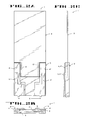
- FIG. 2(a) depicts one of the resonator shapes 1, which are generally rectangular and are oriented so that their shorter sides are parallel to the x-axis of the crystal.
- the resonator shapes are disposed so that their longer sides are parallel to the x-axis, but the former orientation provides better definition of the edges and mounts of the device.
- Two thin gold contacts 4 and 4' are located on both sides of each resonator on a region of the crystal that will eventually form the resonator support structure 3.
- a thicker layer of gold is plated onto the gold contacts at the posterior region of each resonator, forming two contact pads 5 and 5'.
- the contact pads are applied prior to chemical etching and provide rigidity and strength at the resonator's point of attachment to the wafer. This point of attachment can be observed in FIG. 5.
- this gold layer is optional. It should be understood that conductive metals other than gold may be used, and may be applied by methods other than plating without departing from the spirit of the invention.
- the wafer is chemically etched through the crystal to further define the resonator shapes.
- a chemical etch of the metal layer is performed to provide the image of the membrane of each resonator.
- a second quartz etch is then performed to carve out the membranes.
- AT cut crystals have the tendency to form slanted angles during chemical etching. Where these angles are acute or right, continuous metallization from one level of the crystal to the next becomes difficult. It is therefore desirable to shape the aforementioned support structure so that at least one edge on each face between the membrane and support structure will always be obtuse.
- the support structure 3 is U-shaped. In this U-shaped configuration, the crystal forms slopes 6 and 6' on the inside edges of the U-shaped support structure 3. These edges 6 and 6' each provide a gradual slope between the support structure 3 and the membrane 2, thus facilitating metallization later in the process.
- Shapes other than the U-shape may be used which result in at least one sloped edge on each side of the resonator between the support structure and the membrane, such as round or V-shape.
- Chemical etching techniques are well-known and need not be described further.
- the wafer is probed to obtain a sampling of membrane resonating frequencies across the wafer.
- membranes are sampled with a probe arrangement to obtain a range of frequencies representative of the wafer. If the range of frequencies falls below the desired frequency, the wafer is further etched to reduce membrane thicknesses.
- resonating means are applied to each resonator.
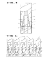
- another coating of thin gold with a chromium adhesion layer is applied to the resonator extending from the U-shaped support structure 3 to the membrane 2 over the sloped edges 6 and 6'.
- This gold-chromium layer forms a contact 13 electrically coupling one of the pads 4 on one side of the resonator to a corresponding gold contact pad 4' on the opposing side.
- Aluminum electrodes 7 and 7' are then provided on opposing sides of the resonator.
- Electrodes are applied overlapping the gold-chromium metallization, using standard masking and etching techniques well-known to artisans. Other means of applying the electrodes may be used, and other conductive materials may be substituted for the aluminum.
- resonating means other than a pair of electrodes may be used without changing the nature of the invention.
- the resonator of the embodiment shown in FIG. 4 has two electrodes 7 and 7' on one face, and a third electrode 7" on the opposing face.
- This type of electrode configuration is designed for use as monolithic crystal filters.
- each crystal resonator is again probed to measure its resonating frequency with the resonating means in place.
- Resonators with frequencies and/or electrical parameters falling outside of an acceptable range are marked and later discarded.
- each resonator is mounted to a header 8.
- Lead terminals 9 from the header are coupled to the resonating means 7 by conductive epoxy or other coupling means.
- a final frequency measurement is taken for each resonator and fine-tuning is performed, by adding mass to the membrane for example.
- the crystal is then encapsulated by a lid sealed to the header.
- the crystal resonator is covered with a cylindrical cap 10 hermetically sealed to the header.
- the container provides protection to the crystal from moisture and contamination. Methods for mounting and sealing crystal resonators are well-known in the art and need not be discussed in detail.
- the packaged resonator is then incorporated into an oscillator circuit (FIG. 7), including an amplifier 11 to amplify the oscillating waveform generated by the crystal, and a feedback circuit 12 for feeding the amplifier output back through the resonator and into the amplifier input until the amplifier is saturated and stable oscillation is achieved.
- an oscillator circuit FIG. 7
- an amplifier 11 to amplify the oscillating waveform generated by the crystal
- a feedback circuit 12 for feeding the amplifier output back through the resonator and into the amplifier input until the amplifier is saturated and stable oscillation is achieved.
Landscapes
- Physics & Mathematics (AREA)
- Acoustics & Sound (AREA)
- Piezo-Electric Or Mechanical Vibrators, Or Delay Or Filter Circuits (AREA)
Applications Claiming Priority (2)
| Application Number | Priority Date | Filing Date | Title |
|---|---|---|---|
| US97302592A | 1992-11-06 | 1992-11-06 | |
| US973025 | 1992-11-06 |
Publications (1)
| Publication Number | Publication Date |
|---|---|
| EP0596522A1 true EP0596522A1 (de) | 1994-05-11 |
Family
ID=25520407
Family Applications (1)
| Application Number | Title | Priority Date | Filing Date |
|---|---|---|---|
| EP93117977A Withdrawn EP0596522A1 (de) | 1992-11-06 | 1993-11-05 | Hochfrequenter Kristallresonator |
Country Status (2)
| Country | Link |
|---|---|
| US (1) | US5436523A (de) |
| EP (1) | EP0596522A1 (de) |
Cited By (1)
| Publication number | Priority date | Publication date | Assignee | Title |
|---|---|---|---|---|
| EP2075911A3 (de) * | 2007-12-28 | 2013-08-28 | Seiko Epson Corporation | Quartzkristall-Resonatorelement, Quartzkristallvorrichtung und Methode zur Herstellung eines Quartzkristall-Resonatorelements |
Families Citing this family (21)
| Publication number | Priority date | Publication date | Assignee | Title |
|---|---|---|---|---|
| JP3148946B2 (ja) * | 1991-05-30 | 2001-03-26 | キヤノン株式会社 | 探針駆動機構並びに該機構を用いたトンネル電流検出装置、情報処理装置、圧電式アクチュエータ |
| US6219531B1 (en) | 1998-09-04 | 2001-04-17 | Ericsson Inc. | Architecture and frequency plan for a UHF portable radio |
| US6201287B1 (en) * | 1998-10-26 | 2001-03-13 | Micron Technology, Inc. | Monolithic inductance-enhancing integrated circuits, complementary metal oxide semiconductor (CMOS) inductance-enhancing integrated circuits, inductor assemblies, and inductance-multiplying methods |
| US6249191B1 (en) | 1998-11-23 | 2001-06-19 | Micron Technology, Inc. | Monolithic integrated circuit oscillators, complementary metal oxide semiconductor (CMOS) voltage-controlled oscillators, integrated circuit oscillators, oscillator-forming methods, and oscillation methods |
| USD526583S1 (en) * | 2004-11-24 | 2006-08-15 | Nihon Dempa Kogyo Co., Ltd. | Crystal resonator for a bio-sensor |
| USD526584S1 (en) * | 2004-11-24 | 2006-08-15 | Nihon Dempa Kogyo Co., Ltd. | Frequency measuring device for a crystal resonator |
| US7259499B2 (en) * | 2004-12-23 | 2007-08-21 | Askew Andy R | Piezoelectric bimorph actuator and method of manufacturing thereof |
| USD540700S1 (en) * | 2005-03-18 | 2007-04-17 | Nihon Dempa Kogyo Co., Ltd. | Crystal resonator for QCM measurement of toxic materials |
| US9722671B2 (en) | 2011-05-27 | 2017-08-01 | uBeam Inc. | Oscillator circuits for wireless power transfer |
| US9819399B2 (en) | 2011-05-27 | 2017-11-14 | uBeam Inc. | Beam interaction control for wireless power transfer |
| US9094111B2 (en) | 2011-05-27 | 2015-07-28 | uBeam Inc. | Receiver transducer for wireless power transfer |
| US9831920B2 (en) | 2011-05-27 | 2017-11-28 | uBeam Inc. | Motion prediction for wireless power transfer |
| US9537322B2 (en) | 2011-05-27 | 2017-01-03 | uBeam Inc. | Sub-apertures with interleaved transmit elements for wireless power transfer |
| US10148131B2 (en) | 2011-05-27 | 2018-12-04 | uBeam Inc. | Power density control for wireless power transfer |
| TW201251157A (en) | 2011-06-03 | 2012-12-16 | Seiko Epson Corp | Piezoelectric vibration element, manufacturing method for piezoelectric vibration element, piezoelectric vibrator, electronic device, and electronic apparatus |
| CN102957394B (zh) * | 2011-08-18 | 2016-12-21 | 精工爱普生株式会社 | 振动元件、振子、电子装置、电子设备、移动体及振动元件的制造方法 |
| US8970316B2 (en) | 2011-08-19 | 2015-03-03 | Seiko Epson Corporation | Resonating element, resonator, electronic device, electronic apparatus, and mobile object |
| US9707593B2 (en) | 2013-03-15 | 2017-07-18 | uBeam Inc. | Ultrasonic transducer |
| US10099253B2 (en) | 2014-12-10 | 2018-10-16 | uBeam Inc. | Transducer with mesa |
| US9736579B2 (en) | 2015-05-20 | 2017-08-15 | uBeam Inc. | Multichannel waveform synthesis engine |
| CN114900152B (zh) * | 2022-05-11 | 2024-11-05 | 铜陵市晶汇电子有限公司 | 一种具有自动补极机构的薄片式晶体谐振器 |
Citations (3)
| Publication number | Priority date | Publication date | Assignee | Title |
|---|---|---|---|---|
| JPS5774626A (en) * | 1980-10-29 | 1982-05-10 | Nippon Denso Co Ltd | Knock sensor |
| EP0092515A1 (de) * | 1982-04-14 | 1983-10-26 | Asulab S.A. | Piezoelektrisches Schwingungselement und dessen Herstellungsverfahren |
| US5023503A (en) * | 1990-01-03 | 1991-06-11 | Motorola, Inc. | Super high frequency oscillator/resonator |
Family Cites Families (23)
| Publication number | Priority date | Publication date | Assignee | Title |
|---|---|---|---|---|
| US2478223A (en) * | 1946-03-01 | 1949-08-09 | Clarkstan Corp | Electrostrictive translator |
| US3721841A (en) * | 1971-06-16 | 1973-03-20 | Motorola Inc | Contact for piezoelectric crystals |
| JPS5123439B2 (de) * | 1971-11-05 | 1976-07-16 | ||
| JPS4979797A (de) * | 1972-12-09 | 1974-08-01 | ||
| JPS5235593A (en) * | 1975-09-13 | 1977-03-18 | Citizen Watch Co Ltd | Shock-proof small-size oscillator |
| JPS5256882A (en) * | 1975-11-05 | 1977-05-10 | Citizen Watch Co Ltd | Supporting structure of crystal vibrator |
| JPS5271189A (en) * | 1975-12-10 | 1977-06-14 | Seiko Epson Corp | Crystal resonator |
| JPS54594A (en) * | 1977-06-03 | 1979-01-05 | Toshiba Corp | Semiconductor device for temperature detecting |
| FR2441960A1 (fr) * | 1978-11-16 | 1980-06-13 | Suisse Horlogerie | Resonateur piezoelectrique travaillant en cisaillement d'epaisseur |
| US4282454A (en) * | 1979-04-27 | 1981-08-04 | Motorola, Inc. | Piezoelectric crystal mounting and connection arrangement |
| CH626479A5 (de) * | 1979-07-05 | 1981-11-13 | Suisse Horlogerie | |
| GB2067009A (en) * | 1979-12-17 | 1981-07-15 | Ebauches Sa | Encapsulated piezo-electric resonator |
| DE3004331C2 (de) * | 1980-02-06 | 1983-06-23 | Siemens AG, 1000 Berlin und 8000 München | Zu Dickenscherungsschwingungen anregbare Resonatorplatte |
| US4494409A (en) * | 1981-05-29 | 1985-01-22 | Kabushiki Kaisha Toyota Chuo Kenkyusho | Engine vibration sensor |
| JPS57206114A (en) * | 1981-06-15 | 1982-12-17 | Seiko Epson Corp | Quartz oscillator |
| JPS58200616A (ja) * | 1982-05-18 | 1983-11-22 | Seiko Instr & Electronics Ltd | 音又型振動子の支持構造 |
| JPS5938621A (ja) * | 1982-08-27 | 1984-03-02 | Nissan Motor Co Ltd | 振動分析装置 |
| JPS58212219A (ja) * | 1983-04-07 | 1983-12-09 | Murata Mfg Co Ltd | チツプ状圧電振動部品 |
| JPS58218214A (ja) * | 1983-05-31 | 1983-12-19 | Murata Mfg Co Ltd | チツプ状圧電振動部品の製造方法 |
| CH655423GA3 (de) * | 1984-02-15 | 1986-04-30 | ||
| US4916413A (en) * | 1987-11-20 | 1990-04-10 | Matsushima Kogyo Kabushiki Kaisha | Package for piezo-oscillator |
| US5285127A (en) * | 1989-11-30 | 1994-02-08 | New Sd, Inc. | Single mode resonator and method |
| US5162691A (en) * | 1991-01-22 | 1992-11-10 | The United States Of America As Represented By The Secretary Of The Army | Cantilevered air-gap type thin film piezoelectric resonator |
-
1993
- 1993-11-05 EP EP93117977A patent/EP0596522A1/de not_active Withdrawn
-
1994
- 1994-05-31 US US08/252,050 patent/US5436523A/en not_active Expired - Lifetime
Patent Citations (3)
| Publication number | Priority date | Publication date | Assignee | Title |
|---|---|---|---|---|
| JPS5774626A (en) * | 1980-10-29 | 1982-05-10 | Nippon Denso Co Ltd | Knock sensor |
| EP0092515A1 (de) * | 1982-04-14 | 1983-10-26 | Asulab S.A. | Piezoelektrisches Schwingungselement und dessen Herstellungsverfahren |
| US5023503A (en) * | 1990-01-03 | 1991-06-11 | Motorola, Inc. | Super high frequency oscillator/resonator |
Non-Patent Citations (1)
| Title |
|---|
| PATENT ABSTRACTS OF JAPAN vol. 006, no. 156 (P - 135) 17 August 1982 (1982-08-17) * |
Cited By (1)
| Publication number | Priority date | Publication date | Assignee | Title |
|---|---|---|---|---|
| EP2075911A3 (de) * | 2007-12-28 | 2013-08-28 | Seiko Epson Corporation | Quartzkristall-Resonatorelement, Quartzkristallvorrichtung und Methode zur Herstellung eines Quartzkristall-Resonatorelements |
Also Published As
| Publication number | Publication date |
|---|---|
| US5436523A (en) | 1995-07-25 |
Similar Documents
| Publication | Publication Date | Title |
|---|---|---|
| US5436523A (en) | High frequency crystal resonator | |
| US5260596A (en) | Monolithic circuit with integrated bulk structure resonator | |
| US4418299A (en) | Face-shear mode quartz crystal vibrators and method of manufacture | |
| EP0641073B1 (de) | Eingekapselter piezoelektrischer Resonator | |
| EP0484545A1 (de) | Elektroden- und elektrodenleitungsstruktur eines piezoelektrischen resonators aus einer ultradünnen schicht | |
| US5376221A (en) | Process for mass producing high frequency crystal resonators | |
| JPS583602B2 (ja) | スイシヨウシンドウシ | |
| EP0483358B1 (de) | Ultradünne quartzkristallfiltereinheit mit mehreren moden | |
| JP3102869B2 (ja) | 超薄板圧電共振子の構造 | |
| JP2000031781A (ja) | 圧電振動子 | |
| JP3543786B2 (ja) | 圧電振動片及び圧電振動子の製造方法 | |
| JP3277501B2 (ja) | 圧電共振子の構造及びその製造方法 | |
| JP2001257560A (ja) | 超薄板圧電振動素子の電極構造 | |
| JP2005033294A (ja) | 水晶振動素子 | |
| JP2003087088A (ja) | 圧電デバイスとその製造方法 | |
| JP2929107B2 (ja) | 水晶振動子の製造方法 | |
| JP2002204140A (ja) | 圧電振動子 | |
| JPS58136125A (ja) | 結合水晶振動子 | |
| JP3102872B2 (ja) | 超薄肉圧電振動子 | |
| JPH11251863A (ja) | 圧電振動子 | |
| JP2001196890A (ja) | 高周波圧電振動子 | |
| JP2001016067A (ja) | バルク波素子及びそれを用いたバルク波装置 | |
| JPH03243008A (ja) | 超薄板水晶共振子の固定方法 | |
| JPS6016108Y2 (ja) | 音叉型水晶振動子 | |
| JPS61258517A (ja) | 圧電振動子 |
Legal Events
| Date | Code | Title | Description |
|---|---|---|---|
| PUAI | Public reference made under article 153(3) epc to a published international application that has entered the european phase |
Free format text: ORIGINAL CODE: 0009012 |
|
| AK | Designated contracting states |
Kind code of ref document: A1 Designated state(s): CH DE FR GB IT LI SE |
|
| 17P | Request for examination filed |
Effective date: 19941018 |
|
| 17Q | First examination report despatched |
Effective date: 19970318 |
|
| GRAG | Despatch of communication of intention to grant |
Free format text: ORIGINAL CODE: EPIDOS AGRA |
|
| GRAG | Despatch of communication of intention to grant |
Free format text: ORIGINAL CODE: EPIDOS AGRA |
|
| GRAH | Despatch of communication of intention to grant a patent |
Free format text: ORIGINAL CODE: EPIDOS IGRA |
|
| STAA | Information on the status of an ep patent application or granted ep patent |
Free format text: STATUS: THE APPLICATION IS DEEMED TO BE WITHDRAWN |
|
| 18D | Application deemed to be withdrawn |
Effective date: 19991023 |