EP0599367A1 - Procédé à faisceau d'ions focalisé et contrôle des charges - Google Patents
Procédé à faisceau d'ions focalisé et contrôle des charges Download PDFInfo
- Publication number
- EP0599367A1 EP0599367A1 EP93203055A EP93203055A EP0599367A1 EP 0599367 A1 EP0599367 A1 EP 0599367A1 EP 93203055 A EP93203055 A EP 93203055A EP 93203055 A EP93203055 A EP 93203055A EP 0599367 A1 EP0599367 A1 EP 0599367A1
- Authority
- EP
- European Patent Office
- Prior art keywords
- specimen
- fib
- conductive
- layer
- surface region
- Prior art date
- Legal status (The legal status is an assumption and is not a legal conclusion. Google has not performed a legal analysis and makes no representation as to the accuracy of the status listed.)
- Granted
Links
Images

Classifications
-
- G—PHYSICS
- G03—PHOTOGRAPHY; CINEMATOGRAPHY; ANALOGOUS TECHNIQUES USING WAVES OTHER THAN OPTICAL WAVES; ELECTROGRAPHY; HOLOGRAPHY
- G03F—PHOTOMECHANICAL PRODUCTION OF TEXTURED OR PATTERNED SURFACES, e.g. FOR PRINTING, FOR PROCESSING OF SEMICONDUCTOR DEVICES; MATERIALS THEREFOR; ORIGINALS THEREFOR; APPARATUS SPECIALLY ADAPTED THEREFOR
- G03F1/00—Originals for photomechanical production of textured or patterned surfaces, e.g., masks, photo-masks, reticles; Mask blanks or pellicles therefor; Containers specially adapted therefor; Preparation thereof
- G03F1/68—Preparation processes not covered by groups G03F1/20 - G03F1/50
- G03F1/72—Repair or correction of mask defects
- G03F1/74—Repair or correction of mask defects by charged particle beam [CPB], e.g. focused ion beam
-
- G—PHYSICS
- G03—PHOTOGRAPHY; CINEMATOGRAPHY; ANALOGOUS TECHNIQUES USING WAVES OTHER THAN OPTICAL WAVES; ELECTROGRAPHY; HOLOGRAPHY
- G03F—PHOTOMECHANICAL PRODUCTION OF TEXTURED OR PATTERNED SURFACES, e.g. FOR PRINTING, FOR PROCESSING OF SEMICONDUCTOR DEVICES; MATERIALS THEREFOR; ORIGINALS THEREFOR; APPARATUS SPECIALLY ADAPTED THEREFOR
- G03F7/00—Photomechanical, e.g. photolithographic, production of textured or patterned surfaces, e.g. printing surfaces; Materials therefor, e.g. comprising photoresists; Apparatus specially adapted therefor
- G03F7/004—Photosensitive materials
- G03F7/09—Photosensitive materials characterised by structural details, e.g. supports, auxiliary layers
- G03F7/093—Photosensitive materials characterised by structural details, e.g. supports, auxiliary layers characterised by antistatic means, e.g. for charge depletion
-
- G—PHYSICS
- G03—PHOTOGRAPHY; CINEMATOGRAPHY; ANALOGOUS TECHNIQUES USING WAVES OTHER THAN OPTICAL WAVES; ELECTROGRAPHY; HOLOGRAPHY
- G03F—PHOTOMECHANICAL PRODUCTION OF TEXTURED OR PATTERNED SURFACES, e.g. FOR PRINTING, FOR PROCESSING OF SEMICONDUCTOR DEVICES; MATERIALS THEREFOR; ORIGINALS THEREFOR; APPARATUS SPECIALLY ADAPTED THEREFOR
- G03F7/00—Photomechanical, e.g. photolithographic, production of textured or patterned surfaces, e.g. printing surfaces; Materials therefor, e.g. comprising photoresists; Apparatus specially adapted therefor
- G03F7/20—Exposure; Apparatus therefor
- G03F7/2051—Exposure without an original mask, e.g. using a programmed deflection of a point source, by scanning, by drawing with a light beam, using an addressed light or corpuscular source
- G03F7/2059—Exposure without an original mask, e.g. using a programmed deflection of a point source, by scanning, by drawing with a light beam, using an addressed light or corpuscular source using a scanning corpuscular radiation beam, e.g. an electron beam
- G03F7/2065—Exposure without an original mask, e.g. using a programmed deflection of a point source, by scanning, by drawing with a light beam, using an addressed light or corpuscular source using a scanning corpuscular radiation beam, e.g. an electron beam using corpuscular radiation other than electron beams
Definitions
- the present invention relates to charged-particle beam processing.
- the present invention relates to methods of controlling charge-up of the target of a charged-particle beam such as a focused-ion beam (FIB) or electron beam.
- a charged-particle beam such as a focused-ion beam (FIB) or electron beam.
- Reticles and masks are used during IC manufacturing to print circuit elements and wiring on silicon. Reticles are also used in the production of masks. Each individual reticle costs on the order of $2000 and typically requires two plus weeks to make. Mask production likewise involves substantial time and expense. The complete circuit patterning for a modern IC will typically require 10 to 20 or more reticles. The ability to modify or repair a reticle or mask quickly is valuable, saving turnaround time and costs.
- Focused ion beams have been used for repair of optical masks and reticles since the mid-1980s.
- Reticles typically consist of an opaque thin film of metal, such as chromium, deposited in a pattern on a transparent substrate of quartz or glass.
- Masks are of similar construction.
- the ability of the FIB to accurately remove unwanted portions of the metal film and to deposit material to "edit" the pattern makes it potentially an almost ideal repair tool.
- the highly-insulating surface of the substrate and the electrically-floating patterns of metal film charge-up when the FIB is applied, causing severe beam drift.
- FIB milling and metal deposition is also used in the semiconductor industry for analysis and repair of integrated circuits.
- an electron flood gun is used to minimize the charging problem and facilitate repair.
- U.S. Patent No. 4,639,301 to Doherty et al . describes a FIB system in which a beam of electrons is directed on the target to neutralize the charge created by the incident ion beam.
- U.S. Patent No. 4,609,809 to Yamaguchi et al . describes a FIB system in which the ion beam is neutralized by an electron shower so as to prevent the wiring portion of an IC from being charged electrically.
- U.S. Patent No. 4,503,329 to Yamaguchi et al describes an arrangement for ion beam machining of mask defects in which electron shower units are provided for neutralizing the ion beam. Alternatively, the electron shower units are directed to the surface of the specimen to prevent charging.
- a prober attached to a grounded arm is placed in contact with a mask pattern, for discharge to ground of charges on the pattern when the ion beam is projected onto the specimen.
- the entire surface of the mask substrate is coated with a thin film of metal or conductive compound such as In2O3 or SnO2 by evaporation. In this arrangement, charges on the mask pattern can be discharged to ground through a conductive clamp which fixes the substrate in a specimen tray.
- FIB FIB
- electron-beam systems it is known to deposit a thin conducting layer of material (usually gold or carbon) on a sample prior to imaging to prevent surface charging by providing a leakage path to ground for surface charge.
- the coating is evaporated onto the specimen in a deposition chamber, after which the specimen is mounted (with suitable electrical contact from the conducting layer to ground) in the vacuum chamber of the FIB or electron-beam system for imaging.
- U.S. Patent No. 5,028,780 to Kaito et al discloses use of FIB and a source of W(CO)6 gas to deposit a tungsten film locally in an area of the specimen where a trench is to be cut to expose a section for observation.
- the deposited tungsten film serves to level the top face of the sample in the area and to avoid distortion of the section which would otherwise be caused by redeposition of sputtered material.
- a prober in contact with a mask pattern also has drawbacks.
- the cost and complexity of operating a prober within the evacuated specimen chamber is a consideration.
- a probe in contact with one portion of the pattern may not adequately discharge the surface charges on the mask if adjacent portions of the pattern and the insulative substrate are allowed to charge-up as the ion beam is applied.
- Evaporating conductive coatings onto the specimen also has drawbacks. Additional equipment is required for deposition and/or removal of the coating. The coating may interfere with bonding of material to be deposited when effecting a repair, and can be difficult to remove. Typically, a carbon coat can be removed from the surface of an IC specimen with an oxygen plasma, but semiconductor manufacturers are reluctant to expose reticles to an oxygen plasma as it adds an additional complex and time consuming handling step and may degrade the optical qualities of the substrate.
- the present invention offers a simple and inexpensive technique for controlling charge-up of a specimen during processing with a FIB or electron-beam system.
- the technique is particularly suitable for FIB modification and repair of masks and reticles used in semiconductor device manufacture.
- an anti-static material such as a volatile fluid containing dimethyl ammonium salt
- a volatile fluid containing dimethyl ammonium salt is applied to the reticle, mask or other specimen of interest prior to beginning repair operations in a FIB system.
- the volatile fluid is allowed to evaporate, leaving a conductive layer of anti-static material.
- the FIB is used to cut through the layer of anti-static material before commencing FIB deposition, to assure proper bonding of deposited repair material.
- a FIB system suitable for carrying out the methods of the present invention is the IDS 7000 FIBstationTM, available commercially from Schlumberger Technologies, Inc., of San Jose, California. Such a system is described, for example, in U.S. Patent No. 5,140,164 to Talbot et al ., the content of which is incorporated herein by this reference.
- an anti-static fluid is applied to a specimen to form a thin conducting layer for neutralization of charge build-up from an incident charged-particle beam.
- the anti-static fluid comprises a conductive material, such as dimethyl ammonium salts, in a volatile liquid carrier, such as water and/or alcohol.
- a conductive material such as dimethyl ammonium salts
- a volatile liquid carrier such as water and/or alcohol.
- the anti-static fluid is preferably capable of being applied to the specimen by swabbing or spraying under room ambient conditions, and rapidly air-dried to form on the specimen a mildly conductive layer having sheet resistance of less than about 1012 ohms/square, preferably less than about 109 ohms/square.
- the conductive layer must remain at least mildly conductive in the vacuum environment of a FIB or e-beam system, and should be readily removable from the specimen using common solvents under room ambient conditions without need for special equipment, e.g. , by rinsing with isopropyl alcohol or water.
- a sheet resistance value of 109 ohms/square with a conductive layer thickness of 1 ⁇ m corresponds to a bulk resistivity of 1011 ⁇ -ohm-cm.
- a preferred anti-static fluid is "Staticide® General Purpose #2001," commercially available from ACL Incorporated of Elk Grove Village, Illinois. "Staticide” is a registered trademark of ACL Incorporated.
- Active ingredients of Staticide® General Purpose #2001 are modified N-Alkyl Dimethyl Ammonium Salts (1.36%), N-alkyl Dimethyl Benzyl Ammonium Salts (.06%), and N-Alkyl Dimethyl Ethyl Benzyl Ammonium Salts (.06%).
- ACL Incorporated quote sheet resistances of Staticide® General Purpose #2001 from 106 ohms/square to 1012 ohms/square depending on conditions of the surface to which it is applied.
- the anti-static fluid is applied to the surface of the specimen with a cotton swab, or is sprayed on or is applied in any other suitable manner.
- the volatile liquid carrier is then allowed to evaporate ( e.g ., by air-drying or by application of a stream of air), leaving a thin layer of the conductive material on the surface of the specimen in the region where the repair is to be made. While thickness of the layer of conductive material is generally not critical, it has been found that a layer of approximately 1 ⁇ m thickness is suitable for reticle repair and is readily achieved by application of the anti-static fluid with a cotton swab.
- a dynamic equilibrium between milling with a FIB and the redeposition of milled material of the region being milled can arise when the depth of a hole milled with a FIB becomes much larger than the diameter of the milled hole ( e.g ., depth/diameter greater than about 6/1), unless a gas is injected to enhance the FIB milling rate.
- the remaining layer of conductive material preferably has a low vapor pressure to allow good vacuum in the FIB chamber.
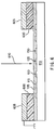
- FIG. 1 is a schematic sectional view of a portion of a reticle 100 on the surface of which is a thin layer 105 of conductive material applied in accordance with the invention.
- Reticle 100 comprises a transparent, insulative substrate 110 (e.g ., of quartz) having an opaque pattern (e.g ., of chromium) deposited on one face. As illustrated, the pattern comprises a series of traces 115, 120, 125 and 130.
- Reticle 100 with the applied layer 105 of conductive material, is placed in the vacuum chamber (not illustrated) of a FIB system.
- Conductive layer 105 may be grounded as will be explained below.
- the chamber is evacuated, and a FIB is then raster-scanned to pre-sputter the region of the specimen where repair is to be made, to locally remove the layer 105 of conductive material in the region where material is to be cut or deposited. Pre-sputtering usually takes a few tens of seconds, depending on the area to be exposed, the FIB beam current level and the type of anti-static fluid employed.
- FIB end-point detection techniques work well (e.g ., monitoring for change in the secondary particle count, most frequently electrons) and provides a clear signal when the surface of the reticle is exposed. Scanning of the FIB is shown schematically by lines 200 in Figure 2. In the illustration of Figure 2, the FIB has been used to remove a portion of conductive layer 105 to expose chromium traces 120 and 125 and the region of substrate 110 lying between them.
- Suitable material can then be introduced in the vacuum chamber as the FIB is raster-scanned over the region where the repair is to be made, to cause deposition of opaque material in a manner known in the art.
- opaque material 305 is deposited as the FIB is scanned over the region as shown by lines 300.
- the FIB can also be used to remove opaque material in prior-art fashion. As shown in Figure 4, a portion of the opaque pattern (in this example, trace 120) is removed by scanning of the FIB over the region as shown by lines 400.
- Figure 5 shows the repaired reticle of Figure 3 following removal of conductive layer 105.
- conductive layer 105 may be grounded, though such grounding may not always be necessary.
- the anti-static material of conductive layer 105 may itself have sufficient charge-gathering capability.
- charge leakage at the edges of conductive layer 105 increases as the area of conductive layer 105 increases. If a large enough area of the specimen is covered with the conductive layer 105 relative to the area of the specimen to be worked with the charged-particle beam, such charge-gathering and charge leakage may not need to be supplemented with grounding of conductive layer 105.
- Figure 6 illustrates a preferred method of grounding conductive layer 105 in the event such grounding is necessary or desired.
- a layer of conductive foam 600 having a central opening e.g ., 1 ⁇ 1 cm opening
- Conductive foam 600 is held firmly in place by a grounded, metal pressure plate 605.
- the combination of conductive layer 105, conductive foam 605 and grounded pressure plate 605 provide a good leakage path to ground for surface charge, thus preventing beam drift.
- the FIB is shown at 610.
- conductive foam material 600 which may be used is a foam material having a silicone elastomer binder with a conductive filler of silver, commercially available under the trade name CHO-FOAM 1501 from Chomerics Inc. of Woburn, Massachusetts.
- Other suitable materials may be used in place of conductive foam material, such as an elastomeric conductive polymer interconnect (ECPI) material.
- ECPI materials are available from the Engineering Research Center of AT&T Bell Laboratories, Hocewell, New Jersey.
- a key advantage of using anti-static fluid in accordance with the invention to apply a conductive layer for neutralizing charge is that, unlike prior-art surface films of carbon or metal, the conductive layer 105 is easily removed with a solvent.
- a solvent For example, isopropyl alcohol works well as a solvent for removing dimethyl ammonium salts .
- removal of conductive layer 105 after repair adds no steps to the overall process as the reticle is always thoroughly cleaned prior to return to the fabrication line for actual use.
- Another advantage of using anti-static fluid in accordance with the invention arises from the fact that, during FIB imaging, the upper surface of conductive layer 105 is exposed to the beam. Extended exposure of the quartz substrate's surface to the FIB degrades the optical qualities of the surface and can cause problems during printing. Conductive layer 105 in this way acts as a protective coating during the FIB repair process.
- a reticle was to be repaired by depositing an opaque line ("strap") to interconnect two opaque regions.
- the reticle was coated with a layer of anti-static fluid, Staticide® General Purpose #2001, applied with a Q-Tip cotton swab and allowed to air dry for about 1/2 minute.
- the reticle was placed in the FIB chamber and conductive foam was used to establish electrical connection from the conductive salt layer on the reticle to a ground conductor. After evacuating the chamber, the FIB was operated to sputter away the conductive dimethyl ammonium salt layer overlying the region where opaque material was to be deposited to effect the repair.
- a 5 ⁇ 5 ⁇ m hole was sputtered through the conductive salt layer overlying each of the two opaque regions, and then a trench was sputtered through the conductive salt layer overlying the area joining the two opaque regions.
- the 5 ⁇ 5 ⁇ m holes were sputtered through the conductive salt layer in about 4 seconds with a beam current density of about 5 A/cm2, a FIB current of about 500 picoamperes, and a spot size of about 100-150 nanometers.
- the trench was sputtered with a FIB current of about 6 nanoamperes and a spot size of about 250 nanometers.
- the FIB currents which determine spot size, were selected based on the reticle feature size, which in this case was 5 ⁇ the feature size of the mask and IC to be produced from the reticle. Lower beam current and a smaller spot size would be used for features of smaller dimension.
- Removal of the conductive salt layer in the region where opaque material is to be deposited assures proper bonding of the deposited opaque material to the reticle and reduces the possibility of the deposited opaque material being damaged or washed away when the conductive salt layer is later removed.
- Opaque metallic platinum was then deposited in the holes and the trench by introducing trimethyl-methyl-cyclo-penta-dienyl-platinum gas in the presence of the FIB.
- the platinum strap covering a 40 ⁇ 8 ⁇ m region, was deposited using a FIB current of about 2 nanoamperes for about 10 minutes.
- the deposit was examined by FIB imaging and with an optical microscope, and was determined to be a successful repair as evidenced by opacity of the reticle in the region of the strap. No problem was encountered with FIB drift or specimen surface charging, as evidenced by a stable FIB image on the display screen.
- the conductive layer of dimethyl ammonium salt was removed with isopropyl alcohol after reticle repair.
- a specimen when using a FIB or electron beam to image the specimen.
- the anti-static fluid is applied and allowed to dry prior to sectioning of a specimen (e.g., an IC specimen), leaving a thin layer of conductive material on the surface of the specimen.
- the specimen can then be sectioned using a FIB or by mechanical milling, and the cut face of the section imaged using a FIB or electron beam.
- a specimen can be sectioned with a FIB by scanning the FIB in a plane passing through the specimen.
- a leakage path is preferably provided from the layer of conductive material.
- a leakage path is preferably provided from the layer of conductive material (for example, as shown in Figure 6) as the FIB or electron beam is scanned over the cut face of the sectioned specimen (with the beam impinging generally perpendicular to the cut face), and secondary particles (electrons or ions) are detected to produce a signal from which an image of the cut face of the section is generated.
- reticle is intended to include a reticle or mask or similar structure comprising essentially a transparent insulative substrate (e.g ., of glass or quartz) having a pattern of opaque material (e.g ., of chromium) deposited thereon.
- transparent insulative substrate e.g ., of glass or quartz
- opaque material e.g ., of chromium
- specimen is intended to include a reticle, mask or similar structure, or an integrated circuit (IC) or multi-chip module (MCM) or other device.
- IC integrated circuit
- MCM multi-chip module
Landscapes
- Physics & Mathematics (AREA)
- General Physics & Mathematics (AREA)
- Health & Medical Sciences (AREA)
- Toxicology (AREA)
- Engineering & Computer Science (AREA)
- Architecture (AREA)
- Structural Engineering (AREA)
- Preparing Plates And Mask In Photomechanical Process (AREA)
- Electron Beam Exposure (AREA)
- Drying Of Semiconductors (AREA)
Applications Claiming Priority (2)
| Application Number | Priority Date | Filing Date | Title |
|---|---|---|---|
| US07/980,371 US5357116A (en) | 1992-11-23 | 1992-11-23 | Focused ion beam processing with charge control |
| US980371 | 1992-11-23 |
Publications (2)
| Publication Number | Publication Date |
|---|---|
| EP0599367A1 true EP0599367A1 (fr) | 1994-06-01 |
| EP0599367B1 EP0599367B1 (fr) | 1996-05-15 |
Family
ID=25527513
Family Applications (1)
| Application Number | Title | Priority Date | Filing Date |
|---|---|---|---|
| EP93203055A Expired - Lifetime EP0599367B1 (fr) | 1992-11-23 | 1993-11-02 | Procédé à faisceau d'ions focalisé et contrÔle des charges |
Country Status (4)
| Country | Link |
|---|---|
| US (1) | US5357116A (fr) |
| EP (1) | EP0599367B1 (fr) |
| JP (1) | JP3263503B2 (fr) |
| DE (1) | DE69302662T2 (fr) |
Cited By (2)
| Publication number | Priority date | Publication date | Assignee | Title |
|---|---|---|---|---|
| EP0961168A1 (fr) * | 1998-05-18 | 1999-12-01 | International Business Machines Corporation | Méthode pour réparer des masques de photogravure |
| CN100397609C (zh) * | 2006-08-04 | 2008-06-25 | 北京中星微电子有限公司 | 一种聚焦离子束修改集成电路的方法及集成电路 |
Families Citing this family (16)
| Publication number | Priority date | Publication date | Assignee | Title |
|---|---|---|---|---|
| US5843623A (en) * | 1996-09-10 | 1998-12-01 | International Business Machines Corporation | Low profile substrate ground probe |
| US6165649A (en) * | 1997-01-21 | 2000-12-26 | International Business Machines Corporation | Methods for repair of photomasks |
| JPH11154479A (ja) * | 1997-11-20 | 1999-06-08 | Hitachi Ltd | 2次電子画像検出方法及びその装置並びに集束荷電粒子ビームによる処理方法及びその装置 |
| US6140581A (en) * | 1997-12-03 | 2000-10-31 | Mitsubishi Electronics America, Inc. | Grounded packaged semiconductor structure and manufacturing method therefor |
| US6030731A (en) * | 1998-11-12 | 2000-02-29 | Micron Technology, Inc. | Method for removing the carbon halo caused by FIB clear defect repair of a photomask |
| US6096459A (en) * | 1998-12-28 | 2000-08-01 | Micron Technology, Inc. | Method for repairing alternating phase shifting masks |
| US6114073A (en) * | 1998-12-28 | 2000-09-05 | Micron Technology, Inc. | Method for repairing phase shifting masks |
| US6277526B1 (en) | 1998-12-28 | 2001-08-21 | Micron Technology, Inc. | Method for repairing MoSi attenuated phase shift masks |
| US6103430A (en) * | 1998-12-30 | 2000-08-15 | Micron Technology, Inc. | Method for repairing bump and divot defects in a phase shifting mask |
| US6458634B1 (en) | 2001-04-18 | 2002-10-01 | International Business Machines Corporation | Reduction of induced charge in SOI devices during focused ion beam processing |
| US6627363B1 (en) | 2002-07-17 | 2003-09-30 | Taiwan Semiconductor Manufacturing Company | Utilizing vacuum ultraviolet (VUV) exposure to remove halos of carbon deposition in clear reticle repair |
| US6869733B1 (en) | 2002-09-30 | 2005-03-22 | Taiwan Semiconductor Manufacturing Company | Pellicle with anti-static/dissipative material coating to prevent electrostatic damage on masks |
| US7514184B2 (en) * | 2002-10-18 | 2009-04-07 | Taiwan Semiconductor Manufacturing Co. | Reticle with antistatic coating |
| JP4253553B2 (ja) * | 2003-09-29 | 2009-04-15 | 株式会社日立ハイテクノロジーズ | 荷電粒子線を用いた成膜方法と選択エッチング方法および荷電粒子線装置 |
| JP4565235B2 (ja) * | 2004-10-22 | 2010-10-20 | 財団法人北九州産業学術推進機構 | 誘電体材料の加工方法 |
| JP5098138B2 (ja) * | 2005-07-11 | 2012-12-12 | 富士通セミコンダクター株式会社 | スパッタリング方法及びスパッタリング装置 |
Citations (3)
| Publication number | Priority date | Publication date | Assignee | Title |
|---|---|---|---|---|
| US4503329A (en) * | 1981-09-30 | 1985-03-05 | Hitachi, Ltd. | Ion beam processing apparatus and method of correcting mask defects |
| EP0459255A2 (fr) * | 1990-05-30 | 1991-12-04 | Hitachi, Ltd. | Procédé pour éviter l'accumulation des charges électriques |
| US5139922A (en) * | 1987-04-10 | 1992-08-18 | Matsushita Electronics Corporation | Method of making resist pattern |
Family Cites Families (8)
| Publication number | Priority date | Publication date | Assignee | Title |
|---|---|---|---|---|
| US4419203A (en) * | 1982-03-05 | 1983-12-06 | International Business Machines Corporation | Apparatus and method for neutralizing ion beams |
| JPS59168652A (ja) * | 1983-03-16 | 1984-09-22 | Hitachi Ltd | 素子修正方法及びその装置 |
| US4564880A (en) * | 1984-03-14 | 1986-01-14 | Motorola, Inc. | Apparatus and method for protecting integrated circuits |
| US4639301B2 (en) * | 1985-04-24 | 1999-05-04 | Micrion Corp | Focused ion beam processing |
| US4910499A (en) * | 1986-09-29 | 1990-03-20 | Monarch Marking Systems, Inc. | Tag and method of making same |
| US4846922A (en) * | 1986-09-29 | 1989-07-11 | Monarch Marking Systems, Inc. | Method of making deactivatable tags |
| JP2779414B2 (ja) * | 1988-12-01 | 1998-07-23 | セイコーインスツルメンツ株式会社 | ミクロ断面の加工・観察方法 |
| US5140164A (en) * | 1991-01-14 | 1992-08-18 | Schlumberger Technologies, Inc. | Ic modification with focused ion beam system |
-
1992
- 1992-11-23 US US07/980,371 patent/US5357116A/en not_active Expired - Fee Related
-
1993
- 1993-11-02 EP EP93203055A patent/EP0599367B1/fr not_active Expired - Lifetime
- 1993-11-02 DE DE69302662T patent/DE69302662T2/de not_active Expired - Fee Related
- 1993-11-22 JP JP29222093A patent/JP3263503B2/ja not_active Expired - Fee Related
Patent Citations (3)
| Publication number | Priority date | Publication date | Assignee | Title |
|---|---|---|---|---|
| US4503329A (en) * | 1981-09-30 | 1985-03-05 | Hitachi, Ltd. | Ion beam processing apparatus and method of correcting mask defects |
| US5139922A (en) * | 1987-04-10 | 1992-08-18 | Matsushita Electronics Corporation | Method of making resist pattern |
| EP0459255A2 (fr) * | 1990-05-30 | 1991-12-04 | Hitachi, Ltd. | Procédé pour éviter l'accumulation des charges électriques |
Cited By (2)
| Publication number | Priority date | Publication date | Assignee | Title |
|---|---|---|---|---|
| EP0961168A1 (fr) * | 1998-05-18 | 1999-12-01 | International Business Machines Corporation | Méthode pour réparer des masques de photogravure |
| CN100397609C (zh) * | 2006-08-04 | 2008-06-25 | 北京中星微电子有限公司 | 一种聚焦离子束修改集成电路的方法及集成电路 |
Also Published As
| Publication number | Publication date |
|---|---|
| DE69302662D1 (de) | 1996-06-20 |
| DE69302662T2 (de) | 1996-12-05 |
| EP0599367B1 (fr) | 1996-05-15 |
| JPH0729819A (ja) | 1995-01-31 |
| JP3263503B2 (ja) | 2002-03-04 |
| US5357116A (en) | 1994-10-18 |
Similar Documents
| Publication | Publication Date | Title |
|---|---|---|
| EP0599367B1 (fr) | Procédé à faisceau d'ions focalisé et contrÔle des charges | |
| JP5090255B2 (ja) | 原位置でのstemサンプル作製方法 | |
| EP0951578B1 (fr) | Systeme de decapage et de depot de revetements de precision | |
| EP0075949B1 (fr) | Appareil de traitement par faisceau d'ions et méthode de correction de défauts de masque | |
| US5035787A (en) | Method for repairing semiconductor masks and reticles | |
| Liu et al. | Resist charging in electron beam lithography | |
| EP2287883B1 (fr) | Dispositif et méthode d'inspection ou de modification d'une surface à l'aide d'un faisceau de particules chargées | |
| KR100373774B1 (ko) | 스테이지로부터 미세 먼지를 제거하는 방법 및 클리닝 판 | |
| USRE33193E (en) | Ion beam processing apparatus and method of correcting mask defects | |
| US5165954A (en) | Method for repairing semiconductor masks & reticles | |
| JP3216881B2 (ja) | 試料断面観察方法 | |
| JP3230180B2 (ja) | 試験品処理方式 | |
| US6525317B1 (en) | Reduction of charging effect and carbon deposition caused by electron beam devices | |
| JP4943629B2 (ja) | ターゲット修復用のイオンビーム | |
| NL8103848A (nl) | Werkwijze voor het vervaardigen van geintegreerde ketens. | |
| JP2973211B2 (ja) | 断面観察方法 | |
| US5178738A (en) | Ion-beam sputtering apparatus and method for operating the same | |
| EP0128242A2 (fr) | Methode de gravure pour structurer un film de polymère dans un appareil de gravure par plasma. | |
| JP3018041B2 (ja) | イオンビーム加工装置 | |
| US6420703B1 (en) | Method for forming a critical dimension SEM calibration standard of improved definition and standard formed | |
| US5628870A (en) | Method for marking a substrate using ionized gas | |
| JPH10241618A (ja) | 荷電ビームによる観察,加工方法及びその装置 | |
| KR20240089292A (ko) | 전자 빔 검사 장치 및 검사 방법 | |
| JP2834243B2 (ja) | 電子線描画における帯電防止方法 | |
| JPS6136928A (ja) | 真空装置 |
Legal Events
| Date | Code | Title | Description |
|---|---|---|---|
| PUAI | Public reference made under article 153(3) epc to a published international application that has entered the european phase |
Free format text: ORIGINAL CODE: 0009012 |
|
| AK | Designated contracting states |
Kind code of ref document: A1 Designated state(s): DE FR GB IT NL |
|
| 17P | Request for examination filed |
Effective date: 19940930 |
|
| 17Q | First examination report despatched |
Effective date: 19941206 |
|
| GRAH | Despatch of communication of intention to grant a patent |
Free format text: ORIGINAL CODE: EPIDOS IGRA |
|
| GRAA | (expected) grant |
Free format text: ORIGINAL CODE: 0009210 |
|
| AK | Designated contracting states |
Kind code of ref document: B1 Designated state(s): DE FR GB IT NL |
|
| PG25 | Lapsed in a contracting state [announced via postgrant information from national office to epo] |
Ref country code: NL Free format text: LAPSE BECAUSE OF FAILURE TO SUBMIT A TRANSLATION OF THE DESCRIPTION OR TO PAY THE FEE WITHIN THE PRESCRIBED TIME-LIMIT Effective date: 19960515 Ref country code: IT Free format text: LAPSE BECAUSE OF FAILURE TO SUBMIT A TRANSLATION OF THE DESCRIPTION OR TO PAY THE FEE WITHIN THE PRE;WARNING: LAPSES OF ITALIAN PATENTS WITH EFFECTIVE DATE BEFORE 2007 MAY HAVE OCCURRED AT ANY TIME BEFORE 2007. THE CORRECT EFFECTIVE DATE MAY BE DIFFERENT FROM THE ONE RECORDED.SCRIBED TIME-LIMIT Effective date: 19960515 |
|
| REF | Corresponds to: |
Ref document number: 69302662 Country of ref document: DE Date of ref document: 19960620 |
|
| ET | Fr: translation filed | ||
| NLV1 | Nl: lapsed or annulled due to failure to fulfill the requirements of art. 29p and 29m of the patents act | ||
| PLBE | No opposition filed within time limit |
Free format text: ORIGINAL CODE: 0009261 |
|
| 26N | No opposition filed | ||
| PG25 | Lapsed in a contracting state [announced via postgrant information from national office to epo] |
Ref country code: GB Free format text: LAPSE BECAUSE OF NON-PAYMENT OF DUE FEES Effective date: 19971102 |
|
| GBPC | Gb: european patent ceased through non-payment of renewal fee |
Effective date: 19971102 |
|
| PGFP | Annual fee paid to national office [announced via postgrant information from national office to epo] |
Ref country code: DE Payment date: 19981231 Year of fee payment: 6 |
|
| PGFP | Annual fee paid to national office [announced via postgrant information from national office to epo] |
Ref country code: FR Payment date: 19991022 Year of fee payment: 7 |
|
| PG25 | Lapsed in a contracting state [announced via postgrant information from national office to epo] |
Ref country code: DE Free format text: LAPSE BECAUSE OF NON-PAYMENT OF DUE FEES Effective date: 20000901 |
|
| PG25 | Lapsed in a contracting state [announced via postgrant information from national office to epo] |
Ref country code: FR Free format text: LAPSE BECAUSE OF NON-PAYMENT OF DUE FEES Effective date: 20010731 |
|
| REG | Reference to a national code |
Ref country code: FR Ref legal event code: ST |