EP0599593A2 - Vollweggleichrichter mit Stromspiegelbrücke - Google Patents
Vollweggleichrichter mit Stromspiegelbrücke Download PDFInfo
- Publication number
- EP0599593A2 EP0599593A2 EP93309314A EP93309314A EP0599593A2 EP 0599593 A2 EP0599593 A2 EP 0599593A2 EP 93309314 A EP93309314 A EP 93309314A EP 93309314 A EP93309314 A EP 93309314A EP 0599593 A2 EP0599593 A2 EP 0599593A2
- Authority
- EP
- European Patent Office
- Prior art keywords
- current
- circuit
- signal
- source
- terminal
- Prior art date
- Legal status (The legal status is an assumption and is not a legal conclusion. Google has not performed a legal analysis and makes no representation as to the accuracy of the status listed.)
- Granted
Links
Images
Classifications
-
- G—PHYSICS
- G01—MEASURING; TESTING
- G01R—MEASURING ELECTRIC VARIABLES; MEASURING MAGNETIC VARIABLES
- G01R19/00—Arrangements for measuring currents or voltages or for indicating presence or sign thereof
- G01R19/22—Arrangements for measuring currents or voltages or for indicating presence or sign thereof using conversion of AC into DC
-
- H—ELECTRICITY
- H02—GENERATION; CONVERSION OR DISTRIBUTION OF ELECTRIC POWER
- H02M—APPARATUS FOR CONVERSION BETWEEN AC AND AC, BETWEEN AC AND DC, OR BETWEEN DC AND DC, AND FOR USE WITH MAINS OR SIMILAR POWER SUPPLY SYSTEMS; CONVERSION OF DC OR AC INPUT POWER INTO SURGE OUTPUT POWER; CONTROL OR REGULATION THEREOF
- H02M7/00—Conversion of AC power input into DC power output; Conversion of DC power input into AC power output
- H02M7/02—Conversion of AC power input into DC power output without possibility of reversal
- H02M7/04—Conversion of AC power input into DC power output without possibility of reversal by static converters
- H02M7/12—Conversion of AC power input into DC power output without possibility of reversal by static converters using discharge tubes with control electrode or semiconductor devices with control electrode
- H02M7/21—Conversion of AC power input into DC power output without possibility of reversal by static converters using discharge tubes with control electrode or semiconductor devices with control electrode using devices of a triode or transistor type requiring continuous application of a control signal
- H02M7/217—Conversion of AC power input into DC power output without possibility of reversal by static converters using discharge tubes with control electrode or semiconductor devices with control electrode using devices of a triode or transistor type requiring continuous application of a control signal using semiconductor devices only
Definitions
- This invention relates to the field of full wave rectifiers.
- this invention relates to the field of rectifying signals with a full wave rectifier having active components.
- signals are rectified in diodes.
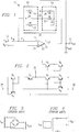
- a full wave rectifier is conventionally mechanized from a diode bridge arrangement as shown in Figure 3.
- a full wave rectifier is conventionally mechanized using a center tapped transformer and diode pair as shown in Figure 4.
- the circuit of Figure 4 is difficult or impossible to produce in an integrated circuit, and the circuit of Figure 3 requires considerable silicon area to integrate and is slow due to high intrinsic parasitic capacities of the diodes.
- a full wave rectifier including an amplifier having a minus input, a plus input and an amplifier output; an input resistor connected between a circuit input and the minus input; and a current bridge having an output terminal connected to the circuit output, a first terminal connected to the minus input and a second terminal connected to the amplifier output, the circuit output driving an output load.
- the current bridge includes a first current mirror circuit and a second current mirror circuit.
- a feedback circuit of a full wave rectifier including a first current mirror circuit connected to an amplifier input and a second current mirror circuit connected to an amplifier output.
- a method for rectifying a signal current applied to a circuit input terminal to provide a rectified signal current at a circuit output of a circuit having a circuit output terminal Considering positive, when the signal current into the circuit input terminal is greater than zero, the method passes a first portion of the signal current from the circuit input terminal to the circuit output terminal and passes a second portion of the signal current from the circuit input terminal to the circuit output, the signal current passing into the circuit input terminal being substantially equal to the sum of the first and second portions of the signal current.
- the method passes the signal current from the circuit output terminal to the circuit input terminal while producing a mirrored current passing from the circuit output terminal to the circuit output, the mirror current being substantially equal to one-half of the signal current.
- full wave rectifier 10 includes amplifier 20, input resistor R IN and current bridge 30.
- Current bridge 30 includes first current mirror circuit 40 and second current mirror circuit 50.
- Current bridge 30 has output terminal 32, first terminal 34 and second terminal 36, terminals 34, 36 being connected to the amplifier.
- Amplifier 20, preferably an amplifier of the type referred to as an operational amplifier, has minus input 22 connected to first terminal 34, plus input 24 connected to a voltage reference V REF , and amplifier output 26 connected to second terminal 36.
- Full wave rectifier 10 has circuit input 12 connected to minus input 22 through input resistor R IN and circuit output 14 connected to output terminal 32.
- amplifier input voltage E IN at minus input 22 will remain at a voltage very nearly equal to reference voltage V REF connected to plus input 24 of amplifier 20.
- This is a basic feature of an operational amplifier where small voltage differences between minus input 22 and plus input 24 are amplified to become a large output signal E OUT at amplifier output 26, and the feedback circuit provides negative feedback to control the amplifier input voltage E IN to be very nearly equal to the reference voltage V REF .
- a signal current will flow from circuit input 12 to minus input 22 (i.e., the amplifier input) which is proportional to the voltage difference V IN -E IN which may be closely approximated by V IN -V REF .
- Substantially all of this current passes through the current bridge 30 since another characteristic of operational amplifiers is a high input impedance so very little current passes into or out of minus input 22.
- the signal current passes from circuit input 12 through input resistor R IN to minus input 22 and then on to first terminal 34. From there a first portion of the signal current passes through first current source 42 from a source end to a drain end and on to second terminal 36 and from there on to amplifier output 26. Meanwhile a second portion of the signal current passes through second current source 44 from a source end to a drain end to output terminal 32 and from there on to circuit output 14.
- First current mirror circuit 40 is preferably designed so that the amount of current passing through second current source 44 is controlled to be equal to the current passing through first current source 42. Therefore, the signal current passing into first terminal 34 is divided equally so that one half passes through each of the first and second current sources 42, 44. It will be appreciated that other proportions of current division may be used as well.
- Second current mirror circuit 50 is preferably designed so that a current passing through third current source 52 controls a mirror current passing through fourth current source 54 from a source end to a drain end to be one half of the current passing through third current source 52.
- the current passing through fourth current source 54 may be another proportion of the current passing through third current source 52 so long as the mirror current passing through fourth current source 54 responsive to the signal current is the same proportion relative to the signal current as the current passing through second current source 44 relative to the signal current.
- the current passing through fourth current source 54 passes to output terminal 32 and from there to circuit output 14.
- Figure 2 is an embodiment of current bridge 30 (i.e., a feedback circuit).
- the first current mirror circuit is represented by transistors Q1 through Q3 and the second current mirror circuit is represented by transistors Q4 through Q8.
- the circuit input terminal 34 is the first terminal 34 of Figure 1
- the circuit output terminal 36 is the second terminal 36 of Figure 1
- the circuit output 32 is the output terminal 32 of Figure 1.
- both transistors preferably pass a portion of the signal current in equal amounts (or in a predetermined ratio of different amounts) through the transistors from the emitter to the collector.
- one half of the signal current passes from circuit input terminal 34 through transistor Q1 to circuit output terminal 36, while the other half of the signal current passes from circuit input terminal 34 through transistor Q2, through transistor Q3 from emitter to collector to circuit output 32.
- the second current mirror circuit is preferably designed such that the current passing from circuit output terminal 36 through transistor Q5 from emitter to collector and from there through transistor Q7 from emitter to collector and from there to circuit output 32 is one half of the signal current passing through transistor Q4 from emitter to collector.
- Transistor Q6 is parallel with transistor Q5 and transistor Q8 is parallel with transistor Q7 (except for the collector of transistor Q8) so that the signal current passing through transistor Q4 will be twice that of the mirror current passing through transistors Q5 and Q7.
- the described rectifier operates with higher precision and speed than conventional rectifiers since the current mirrors employ transistors which do not saturate because of having direct base drive. In addition, fewer components are required in the present invention than used with comparable techniques.
Landscapes
- Engineering & Computer Science (AREA)
- Power Engineering (AREA)
- Physics & Mathematics (AREA)
- General Physics & Mathematics (AREA)
- Rectifiers (AREA)
- Amplifiers (AREA)
- Control Of Electrical Variables (AREA)
Applications Claiming Priority (2)
| Application Number | Priority Date | Filing Date | Title |
|---|---|---|---|
| US07/981,819 US5349521A (en) | 1992-11-25 | 1992-11-25 | Full wave rectifier using a current mirror bridge |
| US981819 | 1992-11-25 |
Publications (3)
| Publication Number | Publication Date |
|---|---|
| EP0599593A2 true EP0599593A2 (de) | 1994-06-01 |
| EP0599593A3 EP0599593A3 (de) | 1995-02-22 |
| EP0599593B1 EP0599593B1 (de) | 1997-06-18 |
Family
ID=25528675
Family Applications (1)
| Application Number | Title | Priority Date | Filing Date |
|---|---|---|---|
| EP93309314A Expired - Lifetime EP0599593B1 (de) | 1992-11-25 | 1993-11-23 | Vollweggleichrichter mit Stromspiegelbrücke |
Country Status (4)
| Country | Link |
|---|---|
| US (2) | US5349521A (de) |
| EP (1) | EP0599593B1 (de) |
| JP (1) | JPH06209576A (de) |
| DE (1) | DE69311684T2 (de) |
Cited By (2)
| Publication number | Priority date | Publication date | Assignee | Title |
|---|---|---|---|---|
| WO1996019261A3 (en) * | 1994-12-19 | 1996-09-06 | Medtronic Inc | Movement powered medical pulse generator having a full-wave rectifier with dynamic bias |
| EP0768747A1 (de) * | 1995-10-09 | 1997-04-16 | STMicroelectronics S.r.l. | Gleichrichtschaltung |
Families Citing this family (4)
| Publication number | Priority date | Publication date | Assignee | Title |
|---|---|---|---|---|
| JP2908282B2 (ja) * | 1995-05-22 | 1999-06-21 | 日本電気移動通信株式会社 | 両波整流回路 |
| US5629641A (en) * | 1996-02-06 | 1997-05-13 | Advanced Micro Devices, Inc. | Differential CMOS current amplifier with controlled bandwidth and common mode distortion |
| US5821790A (en) * | 1996-04-24 | 1998-10-13 | Paragon Electric Company, Inc. | Power line synchronization conditioner |
| US6750702B2 (en) | 2001-12-21 | 2004-06-15 | International Business Machines Corporation | Limiting amplifier |
Family Cites Families (8)
| Publication number | Priority date | Publication date | Assignee | Title |
|---|---|---|---|---|
| JPS5899816A (ja) * | 1981-12-09 | 1983-06-14 | Nec Corp | 整流回路 |
| JPS58146863A (ja) * | 1982-02-25 | 1983-09-01 | Sony Corp | 絶対値検出回路 |
| US4485348A (en) * | 1982-06-01 | 1984-11-27 | Motorola, Inc. | Full wave envelope detector using current mirrors |
| US4523105A (en) * | 1982-09-27 | 1985-06-11 | Rca Corporation | Full wave rectifier circuit for small signals |
| US4636655A (en) * | 1983-11-11 | 1987-01-13 | Kabushiki Kaisha Toshiba | Circuit in which output circuit and operational amplifier equipped input circuit are electrically isolated |
| JPH0782043B2 (ja) * | 1986-02-21 | 1995-09-06 | 株式会社日立製作所 | 整流回路 |
| JPH0770975B2 (ja) * | 1988-01-26 | 1995-07-31 | シャープ株式会社 | 波形変換回路 |
| DE3831454A1 (de) * | 1988-09-16 | 1990-03-29 | Philips Patentverwaltung | Vollweg-gleichrichterschaltung |
-
1992
- 1992-11-25 US US07/981,819 patent/US5349521A/en not_active Expired - Lifetime
-
1993
- 1993-11-23 EP EP93309314A patent/EP0599593B1/de not_active Expired - Lifetime
- 1993-11-23 DE DE69311684T patent/DE69311684T2/de not_active Expired - Fee Related
- 1993-11-25 JP JP5295571A patent/JPH06209576A/ja active Pending
-
1994
- 1994-07-06 US US08/271,043 patent/US5477171A/en not_active Expired - Lifetime
Cited By (5)
| Publication number | Priority date | Publication date | Assignee | Title |
|---|---|---|---|---|
| WO1996019261A3 (en) * | 1994-12-19 | 1996-09-06 | Medtronic Inc | Movement powered medical pulse generator having a full-wave rectifier with dynamic bias |
| EP0974377A1 (de) * | 1994-12-19 | 2000-01-26 | Medtronic, Inc. | Vollwellengleichrichter mit dynamischer Vorspannungsregelung |
| EP0976420A1 (de) * | 1994-12-19 | 2000-02-02 | Medtronic, Inc. | Bewegungsbetriebenes Uhrwerk mit einem Vollwellengleichrichter mit dynamischer Vorspannungsregelung |
| EP0768747A1 (de) * | 1995-10-09 | 1997-04-16 | STMicroelectronics S.r.l. | Gleichrichtschaltung |
| US5812014A (en) * | 1995-10-09 | 1998-09-22 | Sgs-Thomson Microelectronics S.R.L. | Double half-wave rectifier circuit having a wide input dynamic range |
Also Published As
| Publication number | Publication date |
|---|---|
| DE69311684D1 (de) | 1997-07-24 |
| EP0599593A3 (de) | 1995-02-22 |
| EP0599593B1 (de) | 1997-06-18 |
| US5349521A (en) | 1994-09-20 |
| US5477171A (en) | 1995-12-19 |
| JPH06209576A (ja) | 1994-07-26 |
| DE69311684T2 (de) | 1997-12-18 |
Similar Documents
| Publication | Publication Date | Title |
|---|---|---|
| US4808907A (en) | Current regulator and method | |
| KR900005676A (ko) | 전파 정류기 회로 | |
| EP0745923A2 (de) | Spannungsregelung mit Lastpolstabilisation | |
| US4458213A (en) | Constant quiescent current, class AB amplifier output stage | |
| EP0326968A1 (de) | Steuerschaltung mit elektrischen Kenndaten, veränderbar in Abhängigkeit vom Lastwiderstand | |
| EP0028454B1 (de) | Vollweggleichrichter | |
| JPH02162812A (ja) | 相補形カレント・ミラー回路を用いたダイアモンド・フォロワ回路及びゼロ・オフセットの増幅器 | |
| US5027004A (en) | Circuit for regulating the base current of a semiconductor power device | |
| EP0599593A2 (de) | Vollweggleichrichter mit Stromspiegelbrücke | |
| EP0530500B1 (de) | Stromspiegelschaltung | |
| US20030020444A1 (en) | Low drop voltage regulator | |
| KR900007414B1 (ko) | 모터 속도 제어장치 | |
| US4736126A (en) | Trimmable current source | |
| JPH0158684B2 (de) | ||
| JP3554071B2 (ja) | 半導体装置 | |
| US5189380A (en) | Integrated circuit for transducers | |
| KR0112748Y1 (ko) | 전파 정류 회로 | |
| JP3221058B2 (ja) | 整流回路 | |
| EP0087602B1 (de) | Veränderliche Verstärkungsregelungsschaltung | |
| RU2006060C1 (ru) | Источник тока | |
| JPH0364205A (ja) | クリップ回路 | |
| KR920006762Y1 (ko) | Lcd모니터용 전원 콘트롤 회로 | |
| JPH0691402B2 (ja) | 出力クランプ回路 | |
| EP0977105A1 (de) | Regler mit Strombegrenzungsfunktion und Verfahren dazu | |
| JPH0216042B2 (de) |
Legal Events
| Date | Code | Title | Description |
|---|---|---|---|
| PUAI | Public reference made under article 153(3) epc to a published international application that has entered the european phase |
Free format text: ORIGINAL CODE: 0009012 |
|
| AK | Designated contracting states |
Kind code of ref document: A2 Designated state(s): DE FR GB IT |
|
| PUAL | Search report despatched |
Free format text: ORIGINAL CODE: 0009013 |
|
| AK | Designated contracting states |
Kind code of ref document: A3 Designated state(s): DE FR GB IT |
|
| 17P | Request for examination filed |
Effective date: 19950821 |
|
| 17Q | First examination report despatched |
Effective date: 19951228 |
|
| GRAG | Despatch of communication of intention to grant |
Free format text: ORIGINAL CODE: EPIDOS AGRA |
|
| GRAH | Despatch of communication of intention to grant a patent |
Free format text: ORIGINAL CODE: EPIDOS IGRA |
|
| GRAH | Despatch of communication of intention to grant a patent |
Free format text: ORIGINAL CODE: EPIDOS IGRA |
|
| GRAA | (expected) grant |
Free format text: ORIGINAL CODE: 0009210 |
|
| AK | Designated contracting states |
Kind code of ref document: B1 Designated state(s): DE FR GB IT |
|
| REF | Corresponds to: |
Ref document number: 69311684 Country of ref document: DE Date of ref document: 19970724 |
|
| ET | Fr: translation filed | ||
| PGFP | Annual fee paid to national office [announced via postgrant information from national office to epo] |
Ref country code: FR Payment date: 19971112 Year of fee payment: 5 |
|
| PGFP | Annual fee paid to national office [announced via postgrant information from national office to epo] |
Ref country code: GB Payment date: 19971114 Year of fee payment: 5 |
|
| PGFP | Annual fee paid to national office [announced via postgrant information from national office to epo] |
Ref country code: DE Payment date: 19971201 Year of fee payment: 5 |
|
| PLBE | No opposition filed within time limit |
Free format text: ORIGINAL CODE: 0009261 |
|
| 26N | No opposition filed | ||
| PG25 | Lapsed in a contracting state [announced via postgrant information from national office to epo] |
Ref country code: GB Free format text: LAPSE BECAUSE OF NON-PAYMENT OF DUE FEES Effective date: 19981123 |
|
| GBPC | Gb: european patent ceased through non-payment of renewal fee |
Effective date: 19981123 |
|
| PG25 | Lapsed in a contracting state [announced via postgrant information from national office to epo] |
Ref country code: FR Free format text: LAPSE BECAUSE OF NON-PAYMENT OF DUE FEES Effective date: 19990730 |
|
| REG | Reference to a national code |
Ref country code: FR Ref legal event code: ST |
|
| PG25 | Lapsed in a contracting state [announced via postgrant information from national office to epo] |
Ref country code: DE Free format text: LAPSE BECAUSE OF NON-PAYMENT OF DUE FEES Effective date: 19990901 |
|
| PG25 | Lapsed in a contracting state [announced via postgrant information from national office to epo] |
Ref country code: IT Free format text: LAPSE BECAUSE OF NON-PAYMENT OF DUE FEES;WARNING: LAPSES OF ITALIAN PATENTS WITH EFFECTIVE DATE BEFORE 2007 MAY HAVE OCCURRED AT ANY TIME BEFORE 2007. THE CORRECT EFFECTIVE DATE MAY BE DIFFERENT FROM THE ONE RECORDED. Effective date: 20051123 |