EP0600743A2 - Antriebselement mit keramischem Substrat und Tintenstrahldruckkopf mit Benützung derselben - Google Patents
Antriebselement mit keramischem Substrat und Tintenstrahldruckkopf mit Benützung derselben Download PDFInfo
- Publication number
- EP0600743A2 EP0600743A2 EP93309705A EP93309705A EP0600743A2 EP 0600743 A2 EP0600743 A2 EP 0600743A2 EP 93309705 A EP93309705 A EP 93309705A EP 93309705 A EP93309705 A EP 93309705A EP 0600743 A2 EP0600743 A2 EP 0600743A2
- Authority
- EP
- European Patent Office
- Prior art keywords
- actuator
- plate
- ink
- pressure chamber
- ceramic substrate
- Prior art date
- Legal status (The legal status is an assumption and is not a legal conclusion. Google has not performed a legal analysis and makes no representation as to the accuracy of the status listed.)
- Granted
Links
- 239000000758 substrate Substances 0.000 title claims abstract description 73
- 239000000919 ceramic Substances 0.000 title claims abstract description 67
- 125000006850 spacer group Chemical group 0.000 claims abstract description 35
- 230000008859 change Effects 0.000 claims abstract description 9
- 238000004891 communication Methods 0.000 claims description 48
- 238000000034 method Methods 0.000 claims description 15
- 239000012530 fluid Substances 0.000 claims description 9
- MCMNRKCIXSYSNV-UHFFFAOYSA-N Zirconium dioxide Chemical compound O=[Zr]=O MCMNRKCIXSYSNV-UHFFFAOYSA-N 0.000 claims description 4
- PNEYBMLMFCGWSK-UHFFFAOYSA-N aluminium oxide Inorganic materials [O-2].[O-2].[O-2].[Al+3].[Al+3] PNEYBMLMFCGWSK-UHFFFAOYSA-N 0.000 claims description 2
- 239000010419 fine particle Substances 0.000 claims description 2
- 239000000853 adhesive Substances 0.000 description 27
- 230000001070 adhesive effect Effects 0.000 description 27
- 239000000463 material Substances 0.000 description 18
- 239000010408 film Substances 0.000 description 14
- 238000006073 displacement reaction Methods 0.000 description 12
- 238000010304 firing Methods 0.000 description 7
- 230000015572 biosynthetic process Effects 0.000 description 5
- 229910010293 ceramic material Inorganic materials 0.000 description 5
- 238000007641 inkjet printing Methods 0.000 description 5
- 230000004048 modification Effects 0.000 description 5
- 238000012986 modification Methods 0.000 description 5
- 230000000694 effects Effects 0.000 description 4
- 238000004519 manufacturing process Methods 0.000 description 4
- 239000002184 metal Substances 0.000 description 4
- 229910052751 metal Inorganic materials 0.000 description 4
- 230000008569 process Effects 0.000 description 4
- 238000007789 sealing Methods 0.000 description 4
- 230000008901 benefit Effects 0.000 description 3
- 238000004080 punching Methods 0.000 description 3
- 238000007650 screen-printing Methods 0.000 description 3
- YLQBMQCUIZJEEH-UHFFFAOYSA-N Furan Chemical compound C=1C=COC=1 YLQBMQCUIZJEEH-UHFFFAOYSA-N 0.000 description 2
- PXHVJJICTQNCMI-UHFFFAOYSA-N Nickel Chemical compound [Ni] PXHVJJICTQNCMI-UHFFFAOYSA-N 0.000 description 2
- 239000000956 alloy Substances 0.000 description 2
- 229910045601 alloy Inorganic materials 0.000 description 2
- 239000011248 coating agent Substances 0.000 description 2
- 238000000576 coating method Methods 0.000 description 2
- 238000010276 construction Methods 0.000 description 2
- 238000005520 cutting process Methods 0.000 description 2
- 238000010438 heat treatment Methods 0.000 description 2
- 239000012943 hotmelt Substances 0.000 description 2
- 239000000203 mixture Substances 0.000 description 2
- 239000002245 particle Substances 0.000 description 2
- 230000010287 polarization Effects 0.000 description 2
- 229920000728 polyester Polymers 0.000 description 2
- 229920000098 polyolefin Polymers 0.000 description 2
- 238000007639 printing Methods 0.000 description 2
- GHMLBKRAJCXXBS-UHFFFAOYSA-N resorcinol Chemical compound OC1=CC=CC(O)=C1 GHMLBKRAJCXXBS-UHFFFAOYSA-N 0.000 description 2
- 239000002002 slurry Substances 0.000 description 2
- 229920003002 synthetic resin Polymers 0.000 description 2
- 239000000057 synthetic resin Substances 0.000 description 2
- 229920000877 Melamine resin Polymers 0.000 description 1
- ISWSIDIOOBJBQZ-UHFFFAOYSA-N Phenol Chemical compound OC1=CC=CC=C1 ISWSIDIOOBJBQZ-UHFFFAOYSA-N 0.000 description 1
- 239000004952 Polyamide Substances 0.000 description 1
- 239000004642 Polyimide Substances 0.000 description 1
- XSQUKJJJFZCRTK-UHFFFAOYSA-N Urea Chemical compound NC(N)=O XSQUKJJJFZCRTK-UHFFFAOYSA-N 0.000 description 1
- 239000011230 binding agent Substances 0.000 description 1
- 239000004202 carbamide Substances 0.000 description 1
- 230000000052 comparative effect Effects 0.000 description 1
- 239000004020 conductor Substances 0.000 description 1
- 230000008602 contraction Effects 0.000 description 1
- 238000001816 cooling Methods 0.000 description 1
- 239000002178 crystalline material Substances 0.000 description 1
- 230000002950 deficient Effects 0.000 description 1
- 238000007598 dipping method Methods 0.000 description 1
- 238000007599 discharging Methods 0.000 description 1
- 238000009826 distribution Methods 0.000 description 1
- 229920001971 elastomer Polymers 0.000 description 1
- 229920006332 epoxy adhesive Polymers 0.000 description 1
- 229910002112 ferroelectric ceramic material Inorganic materials 0.000 description 1
- 239000000945 filler Substances 0.000 description 1
- 239000011521 glass Substances 0.000 description 1
- 238000000227 grinding Methods 0.000 description 1
- 230000002401 inhibitory effect Effects 0.000 description 1
- 238000001746 injection moulding Methods 0.000 description 1
- 238000009413 insulation Methods 0.000 description 1
- 238000007733 ion plating Methods 0.000 description 1
- 238000010884 ion-beam technique Methods 0.000 description 1
- 238000003754 machining Methods 0.000 description 1
- JDSHMPZPIAZGSV-UHFFFAOYSA-N melamine Chemical compound NC1=NC(N)=NC(N)=N1 JDSHMPZPIAZGSV-UHFFFAOYSA-N 0.000 description 1
- 238000002156 mixing Methods 0.000 description 1
- 238000000465 moulding Methods 0.000 description 1
- 229910052759 nickel Inorganic materials 0.000 description 1
- 230000001590 oxidative effect Effects 0.000 description 1
- 239000004033 plastic Substances 0.000 description 1
- 229920003023 plastic Polymers 0.000 description 1
- 238000007747 plating Methods 0.000 description 1
- 229920002647 polyamide Polymers 0.000 description 1
- 229920001721 polyimide Polymers 0.000 description 1
- 229920001296 polysiloxane Polymers 0.000 description 1
- 229920002635 polyurethane Polymers 0.000 description 1
- 239000004814 polyurethane Substances 0.000 description 1
- 229920005989 resin Polymers 0.000 description 1
- 239000011347 resin Substances 0.000 description 1
- 239000004065 semiconductor Substances 0.000 description 1
- 239000002904 solvent Substances 0.000 description 1
- 238000005507 spraying Methods 0.000 description 1
- 238000004544 sputter deposition Methods 0.000 description 1
- 239000010935 stainless steel Substances 0.000 description 1
- 229910001220 stainless steel Inorganic materials 0.000 description 1
- 239000010409 thin film Substances 0.000 description 1
- 238000007740 vapor deposition Methods 0.000 description 1
Images


Classifications
-
- B—PERFORMING OPERATIONS; TRANSPORTING
- B41—PRINTING; LINING MACHINES; TYPEWRITERS; STAMPS
- B41J—TYPEWRITERS; SELECTIVE PRINTING MECHANISMS, i.e. MECHANISMS PRINTING OTHERWISE THAN FROM A FORME; CORRECTION OF TYPOGRAPHICAL ERRORS
- B41J2/00—Typewriters or selective printing mechanisms characterised by the printing or marking process for which they are designed
- B41J2/005—Typewriters or selective printing mechanisms characterised by the printing or marking process for which they are designed characterised by bringing liquid or particles selectively into contact with a printing material
- B41J2/01—Ink jet
- B41J2/135—Nozzles
- B41J2/14—Structure thereof only for on-demand ink jet heads
- B41J2/14201—Structure of print heads with piezoelectric elements
- B41J2/14233—Structure of print heads with piezoelectric elements of film type, deformed by bending and disposed on a diaphragm
-
- B—PERFORMING OPERATIONS; TRANSPORTING
- B41—PRINTING; LINING MACHINES; TYPEWRITERS; STAMPS
- B41J—TYPEWRITERS; SELECTIVE PRINTING MECHANISMS, i.e. MECHANISMS PRINTING OTHERWISE THAN FROM A FORME; CORRECTION OF TYPOGRAPHICAL ERRORS
- B41J2/00—Typewriters or selective printing mechanisms characterised by the printing or marking process for which they are designed
- B41J2/005—Typewriters or selective printing mechanisms characterised by the printing or marking process for which they are designed characterised by bringing liquid or particles selectively into contact with a printing material
- B41J2/01—Ink jet
- B41J2/135—Nozzles
- B41J2/14—Structure thereof only for on-demand ink jet heads
- B41J2002/14387—Front shooter
Definitions
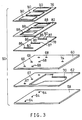
- a metallic nozzle plate 4 having a plurality of nozzles 2 a metallic orifice plate 8 having a plurality of orifices 6, and a channel plate 10 are superposed on each other such that the channel plate 10 is interposed between the plates 4, 8, and these plates 4, 8, 10 are bonded together into an ink nozzle member 16.
- this ink nozzle member 16 there are formed a plurality of ink discharge channels 12 for leading or guiding an ink material to the respective nozzles 2, and at least one ink supply channel 14 for leading or supplying the ink material to the orifices 6.
- an actuator comprising: a ceramic substrate in which at least one pressure chamber is formed, the ceramic substrate including a spacer plate having at least one window which provides the above-indicated at least one pressure chamber, a closure plate superposed on one of opposite major surfaces of the spacer plate, for closing one of opposite openings of each window, and a connecting plate superposed on the other major surface of the spacer plate, for substantially closing the other opening of the window, the connecting plate having at least one slit which corresponds to each pressure chamber, the spacer plate, the closure plate and the connecting plate being formed from respective ceramic green sheets which are laminated on each other and fired into an integral ceramic structure as the ceramic substrate; and at least one piezoelectric/electrostrictive element each disposed on a portion of the closure plate defining the corresponding pressure chamber, for deforming the portion so as to change a pressure of the corresponding pressure chamber, each piezoelectric/electrostrictive element comprising a pair of electrodes and a piezoelectric/elect
- the material for the plates 58, 60, 62 of the ink nozzle member 52 is not particularly limited, these plates 58, 60, 62 are preferably made of a plastic, or a metal such as nickel or stainless steel, which permits highly accurate formation of the nozzles 64 and orifices 68.
- Each of the orifices 68 is desirably formed in tapered shape such that the diameter of the orifice 68 is reduced in the direction of flow of the ink (i.e., in the direction from the ink supply channel 72 toward the pressure chambers 56), as shown in Fig. 1 by way of example, so as to function as a check valve for inhibiting the ink from flowing in the reverse direction.
- the ceramic material for forming the ceramic substrate 84 is not particularly limited, alumina, zirconia or the like may be favorably employed in view of its formability and other properties.
- the closure plate 76, connecting plate 78 and spacer plate 82 are desirably formed from green sheets having substantially the same ceramic composition and distribution in grain size, so as to achieve good sinterability and matching of coefficients of the thermal expansion of the plates 76, 78, 82.
- the thickness of the closure plate 76 is preferably 50 ⁇ m or smaller, more preferably, in a range of about 3 ⁇ 20 ⁇ m.
- the thickness of the connecting plate 78 is preferably 10 ⁇ m or greater, more preferably, 50 ⁇ m or greater.
- the thickness of the spacer plate 82 is preferably 50 ⁇ m or greater, more preferably, 100 ⁇ m or greater.
- the upper and lower electrode films 96, 92 and piezoelectric/electrostrictive layer 94 formed on the closure plate 76 may be heat-treated as needed, either in different steps following formation of the respective films and layer 92, 94, 96, or in one step following formation of all of the films and layer 92, 94, 96.
- the piezoelectric/electrostrictive elements 90 which are supported by the closure plate 76 of the ceramic substrate 84, exhibit sufficiently high mechanical strength and toughness even though the elements 90 have a considerably small thickness.
- the film-forming method used for forming the electrode films 92, 96 and the piezoelectric/electrostrictive layer 94 permits a relatively large number of the piezoelectric/electrostrictive elements 90 to be formed on the closure plate 76. That is, in the film-forming process, the elements 90 can be concurrently and easily formed with a minute spacing left between the adjacent ones, without using an adhesive or the like. Further, in order to assure improved reliability of insulation between the upper and lower electrodes 96, 92, there may be formed as needed an insulating resin layer between the adjacent piezoelectric/electrostrictive layers 94.
- an ink flow channel through which the ink flows through the instant ink jet print head 50 consists of the supply port 74, ink supply channel 72, orifices 68, second communication holes 87, pressure chambers 56, first communication holes 86, through-holes 66, 67 and nozzles 64.
- the adhesive used for bonding the ink nozzle member 52 and the actuator 54 may be selected from various known adhesives, such as those of vinyl-type, acrylic-type and epoxy-type, or those containing polyamide, phenol, resorcinol, urea, melamine, polyester, furan, polyurethane, silicone, rubber, polyimide and polyolefin, provided the selected adhesive is resistant to the ink material.
- the adhesive is in the form of a highly viscous paste which can be applied by coating using a dispenser, or by screen-printing, or is in the form of a sheet which permits punching thereof. It is more desirable to use a hot-melt type adhesive which requires a relatively short heating time, or an adhesive which is curable at room temperature.
- the adhesive in the form of a highly viscous paste may be obtained by mixing an adhesive material with a filler so as to increase the viscosity of the resulting adhesive. It is also desirable to use a highly elastic adhesive so as to increase an amount of deformation of the pressure chambers 56 upon displacement of the piezoelectric/electrostrictive elements 90.
- an elastic epoxy adhesive or silicone-contained adhesive which can be applied by screen-printing, or sheet-like, hot-melt type adhesive containing polyolefin or polyester, which permits punching thereof. It is also possible to apply various adhesives as indicated above to different portions of the bonding surface(s) of the actuator 54 and/or the ink nozzle member 52.
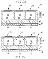
- the pressure chambers 56 of the actuator 54 are held in communication with the nozzles 64 and ink supply channel 72 formed in the ink nozzle member 52, by communicating the first and second communication holes 86, 87 with the through-holes 66 and orifices 68 formed through the orifice plate 60 of the ink nozzle member 52.
- the fluid tightness of the ink flow channel at the bonding surfaces of the actuator 54 and ink nozzle member 52 can be satisfactorily established by providing seals over their regions surrounding the first and second communication holes 86, 87 and the slits 80 connecting the holes 86, 87.
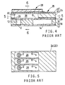
- the present ink jet print head 50 requires a significantly reduced area of the bonding surfaces which must be sealed so as to stably establish a high degree of fluid tightness of the ink flow channel. This advantage will he readily appreciated by comparing the construction of the instant embodiment with that of the known ink jet print head as shown in Figs. 4 and 5, in which a fluid-tight seal between the ink nozzle member 16 and the actuator 25 needs to be provided around the openings of the relatively large voids 22.
- the diameters of the first and second communication holes 86, 87 are set to be smaller than the width dimension of the pressure chamber 56 (the width dimension of the window 88 formed through the spacer plate 82). Therefore, the adjacent ones of the first communication holes 86 and those of the second communication holes 87 are spaced apart from each other by a sufficiently large distance (indicated by "L" in Fig. 2). This arrangement assures a sufficiently large bonding area between the actuator 54 and the ink nozzle member 52, at around the respective first and second communication holes 86, 87. Accordingly, further improved fluid tightness between the bonding surfaces of the actuator 54 and ink nozzle member 52 can be achieved even if these members 54, 52 are made of different kinds of materials.
- the amount of the overflowing adhesive is increased so much as to close the first and second communication holes 86, 87, even in the presence of the slits 80.
- the diameter of the first or second communication holes 86, 87 be set to be substantially equal to the width dimension of the corresponding pressure chamber 56, as shown in Figs. 8a and 8b, so as to avoid the closure of the holes 86, 87 or the ink flow channel.
- the fluid tightness of the ink flow channel can be easily and stable established, and the actuator 54 exhibits improved operating characteristics, due to the formation of the slits 80 in the connecting plate 78. Accordingly, the present print head 50 assures excellent ink-jetting capability with high stability.
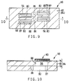
- FIGs. 9 and 10 there will be described an actuator 98 as another embodiment of the present invention.
- the same reference numerals as used in the above description of the actuator 54 of the previous embodiment will be used for identifying structurally and/or functionally corresponding elements, of which no detailed explanation will be provided.
- This actuator 98 has four pressure chambers 56 which are formed in the ceramic substrate 84 in a zigzag fashion, as shown in Fig. 9. Namely, two rows (left and right in Fig. 9) each consisting of two of the pressure chambers 56 are disposed with one of the rows displaced relative to the other row in the width direction of the substrate 84, i.e., in the vertical direction in Fig. 9.
- the first communication holes 86 are formed in the portions of the connecting plate 78 between the left and right rows of the pressure chambers 56, and the slits 80 extend from the respective pressure chambers 56 to the corresponding first communication holes 86.
- the first communication holes 86 can be arranged with increased density, that is, at a pitch substantially equal to or smaller than the width of the pressure chamber 56.
- this actuator 98 is used for an ink jet print head, therefore, the pitch of nozzles that are aligned with the first communication holes 86 can be significantly reduced, whereby the print head is capable of performing highly accurate and high-quality printing.
- the slits 80 provide a part of the ink flow channel through which the ink flows through the print head, and is therefore required to have a sufficiently large width.
- the actuator 98 is modified in respect of the shape of the first communication holes 86, so that the holes 86 are arranged with further increased density or at a narrower pitch.
- the actuator 98 is also modified by providing additional slits 100 on the opposite sides of the pressure chambers 56 as viewed in the direction of the width of the chambers 56, as shown in Figs. 11 and 12a, so as to increase the amount of displacement of the actuator 98.
- these slits 100 are formed in the upper portion of the spacer plate 82 to interpose the upper portion of the pressure chambers 56 therebetween, the rigidity of the ceramic substrate 84 can be advantageously reduced to allow easy deformation of the chambers 56, thereby permitting the actuator 98 to undergo an effectively increased amount of displacement, as shown in Fig. 12b.
- the actuator constructed according to the present invention may be used as an ink pump for ink jet print heads having various other structures, and may also be used for microphones, piezoelectric loudspeakers, sensors, vibrators or resonators, filters and other components or devices.
- the dimensions, shape, number and position of the slits 80 formed in the actuator 54 are not limited to those of the illustrated embodiments, but may be suitably selected provided the slits 80 serve to effectively increase the amount of deformation of the pressure chambers 56. While the ratio of the width of the slits 80 to that of the pressure chambers 56 (i.e., the width of the windows 88 formed in the spacer plate 82) is about 1:3 in the illustrated embodiments, the slits may be formed with almost no width by just cutting the surface of the ceramic substrate 84, so as to yield the above-described effects.
- each of the slits 80 be formed to connect the corresponding first and second communication holes 86, 87 as in the illustrated embodiments, the slit is not necessarily required to connect the holes 86, 87, but may be formed as a plurality of separate slit sections formed between the first and second communication holes 86, 87. Further, the slits 80 may extend in other directions than that of the illustrated embodiments.
Landscapes
- Particle Formation And Scattering Control In Inkjet Printers (AREA)
Applications Claiming Priority (4)
| Application Number | Priority Date | Filing Date | Title |
|---|---|---|---|
| JP350873/92 | 1992-12-04 | ||
| JP35087392 | 1992-12-04 | ||
| JP289257/93 | 1993-11-18 | ||
| JP05289257A JP3106044B2 (ja) | 1992-12-04 | 1993-11-18 | アクチュエータ及びそれを用いたインクジェットプリントヘッド |
Publications (3)
| Publication Number | Publication Date |
|---|---|
| EP0600743A2 true EP0600743A2 (de) | 1994-06-08 |
| EP0600743A3 EP0600743A3 (de) | 1994-08-31 |
| EP0600743B1 EP0600743B1 (de) | 1996-10-16 |
Family
ID=26557529
Family Applications (1)
| Application Number | Title | Priority Date | Filing Date |
|---|---|---|---|
| EP93309705A Expired - Lifetime EP0600743B1 (de) | 1992-12-04 | 1993-12-03 | Antriebselement mit keramischem Substrat und Tintenstrahldruckkopf mit Benützung derselben |
Country Status (5)
| Country | Link |
|---|---|
| US (1) | US5617127A (de) |
| EP (1) | EP0600743B1 (de) |
| JP (1) | JP3106044B2 (de) |
| DE (1) | DE69305477T2 (de) |
| SG (1) | SG48872A1 (de) |
Cited By (13)
| Publication number | Priority date | Publication date | Assignee | Title |
|---|---|---|---|---|
| GB2282992A (en) * | 1993-08-23 | 1995-04-26 | Seiko Epson Corp | Ink jet recording head and method of manufacturing the same. |
| EP0666173A3 (de) * | 1994-02-08 | 1995-12-13 | Sharp Kk | Farbstrahlkopf. |
| WO1996014988A1 (en) * | 1994-11-14 | 1996-05-23 | Philips Electronics N.V. | Ink jet recording device and ink jet recording head |
| EP0750987A1 (de) * | 1995-06-27 | 1997-01-02 | Seiko Epson Corporation | Antrieb für einen Tintenstrahldruckkopf |
| EP0719642A3 (de) * | 1994-12-21 | 1997-04-23 | Seiko Epson Corp | Tintenstrahlaufzeichnungskopf, sein Herstellungsverfahren und Aufzeichnungsvorrichtung |
| EP0785071A4 (de) * | 1995-07-24 | 1997-10-08 | Seiko Epson Corp | Chip des piezoelektrischen/elektrostriktiven types |
| EP0755791A3 (de) * | 1995-07-24 | 1997-11-05 | Seiko Epson Corporation | Antriebseinheit für einen Tintenstrahl-Aufzeichnungskopf und zugehöriges Herstellungsverfahren |
| WO2006037995A3 (en) * | 2004-10-04 | 2006-06-15 | Xaar Technology Ltd | Droplet deposition apparatus |
| US7125097B2 (en) * | 2002-10-04 | 2006-10-24 | Brother Kogyo Kabushiki Kaisha | Ink-jet printing head in which each passage between pressure chamber and nozzle includes horizontally extending portion |
| EP1815991A3 (de) * | 2006-02-01 | 2007-09-12 | Samsung Electronics Co., Ltd. | Piezoelektrischer Tintenstrahldruckkopf |
| EP1842676A3 (de) * | 2006-04-06 | 2009-06-17 | Océ-Technologies B.V. | Druckkopf und Tintenstrahldrucker mit einem derartigen Druckkopf |
| EP2540503A1 (de) * | 2011-06-28 | 2013-01-02 | SII Printek Inc | Flüssigkeitsstrahlkopf, Flüssigkeitsausstoßvorrichtung und Verfahren zur Herstellung des Flüssigkeitsstrahlkopfs |
| EP3825100A1 (de) * | 2019-11-19 | 2021-05-26 | Quantica GmbH | Materialausstosssystem, druckkopf, 3d-drucker und verfahren zur materialausstossung |
Families Citing this family (35)
| Publication number | Priority date | Publication date | Assignee | Title |
|---|---|---|---|---|
| JP3484841B2 (ja) * | 1994-09-26 | 2004-01-06 | セイコーエプソン株式会社 | インクジェット式記録ヘッド |
| JP3196811B2 (ja) * | 1994-10-17 | 2001-08-06 | セイコーエプソン株式会社 | 積層型インクジェット式記録ヘッド、及びその製造方法 |
| JP3501860B2 (ja) * | 1994-12-21 | 2004-03-02 | 日本碍子株式会社 | 圧電/電歪膜型素子及びその製造方法 |
| JP3366146B2 (ja) * | 1995-03-06 | 2003-01-14 | セイコーエプソン株式会社 | インク噴射ヘッド |
| JPH09164705A (ja) * | 1995-12-14 | 1997-06-24 | Mitsubishi Electric Corp | インクジェット記録装置 |
| JP3209082B2 (ja) * | 1996-03-06 | 2001-09-17 | セイコーエプソン株式会社 | 圧電体薄膜素子及びその製造方法、並びにこれを用いたインクジェット式記録ヘッド |
| EP0810676B1 (de) * | 1996-05-27 | 2002-08-28 | Ngk Insulators, Ltd. | Piezoelektrisches Element des Dünnschichttyps |
| EP0839653A3 (de) | 1996-10-29 | 1999-06-30 | Matsushita Electric Industrial Co., Ltd. | Tintenstrahlaufzeichnungsgerät und Verfahren zu seiner Herstellung |
| US5877580A (en) * | 1996-12-23 | 1999-03-02 | Regents Of The University Of California | Micromachined chemical jet dispenser |
| US6494566B1 (en) | 1997-01-31 | 2002-12-17 | Kyocera Corporation | Head member having ultrafine grooves and a method of manufacture thereof |
| JP3592023B2 (ja) * | 1997-03-04 | 2004-11-24 | 日本碍子株式会社 | 機能性膜素子の製造方法 |
| JPH1110861A (ja) * | 1997-06-19 | 1999-01-19 | Brother Ind Ltd | インクジェットプリンタヘッド |
| JP3456380B2 (ja) * | 1997-09-02 | 2003-10-14 | 株式会社村田製作所 | 圧電アクチュエータ |
| JPH11191645A (ja) * | 1997-12-25 | 1999-07-13 | Kyocera Corp | 圧電/電歪膜型アクチュエータ |
| JP3267937B2 (ja) * | 1998-09-04 | 2002-03-25 | 松下電器産業株式会社 | インクジェットヘッド |
| CN100337822C (zh) * | 2000-02-25 | 2007-09-19 | 松下电器产业株式会社 | 喷墨头及喷墨式记录装置 |
| WO2001072519A1 (en) | 2000-03-27 | 2001-10-04 | Fujitsu Limited | Multiple-nozzle ink-jet head and method of manufacture thereof |
| JP2002086725A (ja) * | 2000-07-11 | 2002-03-26 | Matsushita Electric Ind Co Ltd | インクジェットヘッド、その製造方法及びインクジェット式記録装置 |
| CN1369371A (zh) * | 2001-01-30 | 2002-09-18 | 松下电器产业株式会社 | 喷墨头、传动装置的检查方法、喷墨头制造方法和喷墨式记录装置 |
| US7052117B2 (en) * | 2002-07-03 | 2006-05-30 | Dimatix, Inc. | Printhead having a thin pre-fired piezoelectric layer |
| JP2005027404A (ja) * | 2003-06-30 | 2005-01-27 | Kyocera Corp | 圧電アクチュエータ装置及びインクジェットヘッド |
| US8491076B2 (en) | 2004-03-15 | 2013-07-23 | Fujifilm Dimatix, Inc. | Fluid droplet ejection devices and methods |
| US7281778B2 (en) | 2004-03-15 | 2007-10-16 | Fujifilm Dimatix, Inc. | High frequency droplet ejection device and method |
| JP4710491B2 (ja) * | 2004-08-31 | 2011-06-29 | ブラザー工業株式会社 | 液体移送装置 |
| EP1836056B1 (de) | 2004-12-30 | 2018-11-07 | Fujifilm Dimatix, Inc. | Tintenstrahldruck |
| US7468284B2 (en) * | 2005-02-28 | 2008-12-23 | Silverbrook Research Pty Ltd | Method of bonding substrates |
| JP4963555B2 (ja) * | 2005-04-28 | 2012-06-27 | キヤノン株式会社 | インクジェット記録ヘッド |
| JP4506717B2 (ja) * | 2005-07-20 | 2010-07-21 | セイコーエプソン株式会社 | 液滴吐出ヘッド及び液滴吐出装置 |
| US7600863B2 (en) * | 2006-01-04 | 2009-10-13 | Xerox Corporation | Inkjet jet stack external manifold |
| JP4867402B2 (ja) * | 2006-03-06 | 2012-02-01 | 富士ゼロックス株式会社 | 圧電アクチュエータ及び液滴吐出装置及び圧電アクチュエータ製造方法 |
| JP2007276479A (ja) * | 2006-04-06 | 2007-10-25 | Oce Technol Bv | プリントヘッド及びこれを含むインクジェットプリンタ |
| US7988247B2 (en) | 2007-01-11 | 2011-08-02 | Fujifilm Dimatix, Inc. | Ejection of drops having variable drop size from an ink jet printer |
| US20100045740A1 (en) * | 2008-08-19 | 2010-02-25 | Xerox Corporation | Fluid dispensing subassembly with compliant aperture plate |
| JP2012245625A (ja) * | 2011-05-25 | 2012-12-13 | Seiko Epson Corp | 液体噴射ヘッド及び液体噴射装置 |
| ES2472140B2 (es) * | 2014-02-07 | 2015-01-29 | Kerajet S.A. | Método de proyección de sólidos sobre una superficie |
Family Cites Families (23)
| Publication number | Priority date | Publication date | Assignee | Title |
|---|---|---|---|---|
| GB1122245A (en) * | 1966-04-22 | 1968-07-31 | Marconi Co Ltd | Improvements in or relating to electro-mechanical resonators |
| US3946398A (en) * | 1970-06-29 | 1976-03-23 | Silonics, Inc. | Method and apparatus for recording with writing fluids and drop projection means therefor |
| SE349676B (de) * | 1971-01-11 | 1972-10-02 | N Stemme | |
| JPS56172A (en) * | 1979-06-18 | 1981-01-06 | Nec Corp | Ink jet recording head |
| JPS58108164A (ja) * | 1981-12-22 | 1983-06-28 | Seiko Epson Corp | インクジエツトヘツド |
| JPS58137317A (ja) * | 1982-02-09 | 1983-08-15 | Nec Corp | 圧電薄膜複合振動子 |
| JPS58196069A (ja) * | 1982-05-12 | 1983-11-15 | Nec Corp | 電歪効果素子 |
| JPS5932182A (ja) * | 1982-08-16 | 1984-02-21 | Sumitomo Special Metals Co Ltd | バイモルフ用圧電素子 |
| GB2161647A (en) * | 1984-07-10 | 1986-01-15 | Gen Electric Co Plc | Piezoelectric devices |
| JPS61253873A (ja) * | 1985-05-02 | 1986-11-11 | Toshiba Corp | 圧電セラミツク材料 |
| DE3645017C2 (de) * | 1985-09-06 | 1990-07-12 | Fuji Electric Co., Ltd., Kawasaki, Kanagawa, Jp | |
| JPS62135377A (ja) * | 1985-12-09 | 1987-06-18 | Nec Corp | インクジエツトヘツドおよびその製造方法 |
| US4680595A (en) * | 1985-11-06 | 1987-07-14 | Pitney Bowes Inc. | Impulse ink jet print head and method of making same |
| US4769570A (en) * | 1986-04-07 | 1988-09-06 | Toshiba Ceramics Co., Ltd. | Piezo-electric device |
| JPS63285983A (ja) * | 1987-05-18 | 1988-11-22 | Omron Tateisi Electronics Co | 薄膜圧電素子の製造方法 |
| US4783821A (en) * | 1987-11-25 | 1988-11-08 | The Regents Of The University Of California | IC processed piezoelectric microphone |
| US4906840A (en) * | 1988-01-27 | 1990-03-06 | The Board Of Trustees Of Leland Stanford Jr., University | Integrated scanning tunneling microscope |
| JPH01282878A (ja) * | 1988-05-10 | 1989-11-14 | Tosoh Corp | 屈曲型圧電変位素子 |
| DE68906001T2 (de) * | 1988-12-07 | 1993-09-09 | Seiko Epson Corp | Auf abruf arbeitender tintenstrahldruckkopf. |
| DE69125098T2 (de) * | 1990-11-09 | 1997-06-19 | Citizen Watch Co Ltd | Tintenstrahlkopf |
| JP3144949B2 (ja) * | 1992-05-27 | 2001-03-12 | 日本碍子株式会社 | 圧電/電歪アクチュエータ |
| JP3212382B2 (ja) * | 1992-10-01 | 2001-09-25 | 日本碍子株式会社 | 精密ろう付け方法 |
| JP3106026B2 (ja) * | 1993-02-23 | 2000-11-06 | 日本碍子株式会社 | 圧電/電歪アクチュエータ |
-
1993
- 1993-11-18 JP JP05289257A patent/JP3106044B2/ja not_active Expired - Lifetime
- 1993-12-01 US US08/159,922 patent/US5617127A/en not_active Expired - Lifetime
- 1993-12-03 DE DE69305477T patent/DE69305477T2/de not_active Expired - Lifetime
- 1993-12-03 SG SG1996003233A patent/SG48872A1/en unknown
- 1993-12-03 EP EP93309705A patent/EP0600743B1/de not_active Expired - Lifetime
Cited By (31)
| Publication number | Priority date | Publication date | Assignee | Title |
|---|---|---|---|---|
| US5856837A (en) * | 1993-08-23 | 1999-01-05 | Seiko Epson Corporation | Ink jet recording head with vibrating element having greater width than drive electrode |
| US6334673B1 (en) | 1993-08-23 | 2002-01-01 | Seiko Epson Corporation | Ink jet print head with plural electrodes |
| GB2282992B (en) * | 1993-08-23 | 1997-11-26 | Seiko Epson Corp | Ink jet recording head and method of manufacturing the same |
| GB2282992A (en) * | 1993-08-23 | 1995-04-26 | Seiko Epson Corp | Ink jet recording head and method of manufacturing the same. |
| US5956829A (en) * | 1993-08-23 | 1999-09-28 | Seiko Epson Corporation | Method of manufacturing an ink jet recording head |
| EP0666173A3 (de) * | 1994-02-08 | 1995-12-13 | Sharp Kk | Farbstrahlkopf. |
| US5764255A (en) * | 1994-02-08 | 1998-06-09 | Sharp Kabushiki Kaisha | Ink jet head with a deformable piezoelectric vibrating plate |
| WO1996014988A1 (en) * | 1994-11-14 | 1996-05-23 | Philips Electronics N.V. | Ink jet recording device and ink jet recording head |
| EP0719642A3 (de) * | 1994-12-21 | 1997-04-23 | Seiko Epson Corp | Tintenstrahlaufzeichnungskopf, sein Herstellungsverfahren und Aufzeichnungsvorrichtung |
| US6584687B1 (en) | 1994-12-21 | 2003-07-01 | Seiko Epson Corporation | Method of manufacturing an ink-jet recording head using a thermally fusible film that does not close communication holes |
| US5872583A (en) * | 1994-12-21 | 1999-02-16 | Seiko Epson Corporation | Using fusible films having windows supplied with adhesive and gap material |
| EP0750987A1 (de) * | 1995-06-27 | 1997-01-02 | Seiko Epson Corporation | Antrieb für einen Tintenstrahldruckkopf |
| US6033058A (en) * | 1995-06-27 | 2000-03-07 | Seiko Epson Corporation | Actuator for an ink jet print head of the layered type with offset linear arrays of pressure generating chamber |
| EP1034930A1 (de) * | 1995-07-24 | 2000-09-13 | Seiko Epson Corporation | Tintenstrahlaufzeichnungskopf |
| US5907340A (en) * | 1995-07-24 | 1999-05-25 | Seiko Epson Corporation | Laminated ink jet recording head with plural actuator units connected at outermost ends |
| EP0755791A3 (de) * | 1995-07-24 | 1997-11-05 | Seiko Epson Corporation | Antriebseinheit für einen Tintenstrahl-Aufzeichnungskopf und zugehöriges Herstellungsverfahren |
| US6440174B1 (en) | 1995-07-24 | 2002-08-27 | Seiko Epson Corporation | Piezo-electric/electrostrictive film type chip |
| EP0785071A4 (de) * | 1995-07-24 | 1997-10-08 | Seiko Epson Corp | Chip des piezoelektrischen/elektrostriktiven types |
| US7125097B2 (en) * | 2002-10-04 | 2006-10-24 | Brother Kogyo Kabushiki Kaisha | Ink-jet printing head in which each passage between pressure chamber and nozzle includes horizontally extending portion |
| WO2006037995A3 (en) * | 2004-10-04 | 2006-06-15 | Xaar Technology Ltd | Droplet deposition apparatus |
| US7699442B2 (en) | 2006-02-01 | 2010-04-20 | Samsung Electro-Mechanics Co., Ltd | Piezoelectric inkjet printhead |
| EP1815991A3 (de) * | 2006-02-01 | 2007-09-12 | Samsung Electronics Co., Ltd. | Piezoelektrischer Tintenstrahldruckkopf |
| US8042919B2 (en) | 2006-02-01 | 2011-10-25 | Samsung Electro-Mechanics Co., Ltd. | Piezoelectric inkjet printhead |
| EP1842676A3 (de) * | 2006-04-06 | 2009-06-17 | Océ-Technologies B.V. | Druckkopf und Tintenstrahldrucker mit einem derartigen Druckkopf |
| EP2540503A1 (de) * | 2011-06-28 | 2013-01-02 | SII Printek Inc | Flüssigkeitsstrahlkopf, Flüssigkeitsausstoßvorrichtung und Verfahren zur Herstellung des Flüssigkeitsstrahlkopfs |
| CN102848730A (zh) * | 2011-06-28 | 2013-01-02 | 精工电子打印科技有限公司 | 液体喷射头、液体喷射装置以及液体喷射头的制造方法 |
| US8651631B2 (en) | 2011-06-28 | 2014-02-18 | Sii Printek Inc. | Liquid jet head, liquid jet apparatus, and method of manufacturing liquid jet head |
| CN102848730B (zh) * | 2011-06-28 | 2016-08-17 | 精工电子打印科技有限公司 | 液体喷射头、液体喷射装置以及液体喷射头的制造方法 |
| EP3825100A1 (de) * | 2019-11-19 | 2021-05-26 | Quantica GmbH | Materialausstosssystem, druckkopf, 3d-drucker und verfahren zur materialausstossung |
| WO2021099185A1 (en) * | 2019-11-19 | 2021-05-27 | Quantica Gmbh | Material ejection system, print head, 3d printer, and method for material ejection |
| US12030247B2 (en) | 2019-11-19 | 2024-07-09 | Quantica Gmbh | Material ejection system, print head, 3D printer, and method for material ejection |
Also Published As
| Publication number | Publication date |
|---|---|
| DE69305477T2 (de) | 1997-03-13 |
| SG48872A1 (en) | 1998-05-18 |
| JPH06218929A (ja) | 1994-08-09 |
| EP0600743A3 (de) | 1994-08-31 |
| EP0600743B1 (de) | 1996-10-16 |
| JP3106044B2 (ja) | 2000-11-06 |
| DE69305477D1 (de) | 1996-11-21 |
| US5617127A (en) | 1997-04-01 |
Similar Documents
| Publication | Publication Date | Title |
|---|---|---|
| EP0600743B1 (de) | Antriebselement mit keramischem Substrat und Tintenstrahldruckkopf mit Benützung derselben | |
| EP0666605B1 (de) | Piezoelektrischer und/oder elektrostriktiver Antrieb | |
| EP0613196B1 (de) | Piezoelektrischer/elektrostriktiver Antrieb mit keramischem Substrat, das neben Druckkammerfenstern auch Hilfsfenster hat | |
| US6290340B1 (en) | Multi-layer ink jet print head and manufacturing method therefor | |
| EP0572231B1 (de) | Tintenstrahldruckkopf | |
| HK1007056B (en) | Piezoelectric and/or electrostrictive actuator | |
| US5643379A (en) | Method of producing a piezoelectric/electrostrictive actuator | |
| EP0587346B1 (de) | Farbstrahldruckkopf mit Bestandteilen mit verschiedenen Wärme-Ausdehnungskoeffizienten | |
| US7053526B2 (en) | Piezoelectric structure, liquid ejecting head and manufacturing method therefor | |
| EP0732208B1 (de) | Tintendruckkopf mit keramischer Tintenpumpe und damit verbundenem metallischen Düsenkörper | |
| EP1486331B1 (de) | Piezoelektrisches stellglied und dieses aufweisender fluideinspritzkopf | |
| US6910272B2 (en) | Method of manufacturing an ink jet recording head | |
| US6997547B2 (en) | Piezoelectric element, piezoelectric actuator and liquid jetting head incorporating the same | |
| JP3363881B2 (ja) | インクジェットプリントヘッド | |
| HK1001015B (en) | Piezoelectric/electrostrictive actuator having ceramic substrate with auxiliary windows in addition to pressure chamber windows | |
| JP3106030B2 (ja) | 圧電/電歪アクチュエータ | |
| JP4529298B2 (ja) | インクジェットヘッドの製造方法 | |
| JP2001179975A (ja) | 圧電/電歪アクチュエータ |
Legal Events
| Date | Code | Title | Description |
|---|---|---|---|
| PUAI | Public reference made under article 153(3) epc to a published international application that has entered the european phase |
Free format text: ORIGINAL CODE: 0009012 |
|
| 17P | Request for examination filed |
Effective date: 19931220 |
|
| AK | Designated contracting states |
Kind code of ref document: A2 Designated state(s): DE FR GB IT |
|
| PUAL | Search report despatched |
Free format text: ORIGINAL CODE: 0009013 |
|
| AK | Designated contracting states |
Kind code of ref document: A3 Designated state(s): DE FR GB IT |
|
| RAP1 | Party data changed (applicant data changed or rights of an application transferred) |
Owner name: SEIKO EPSON CORPORATION Owner name: NGK INSULATORS, LTD. |
|
| GRAG | Despatch of communication of intention to grant |
Free format text: ORIGINAL CODE: EPIDOS AGRA |
|
| 17Q | First examination report despatched |
Effective date: 19951215 |
|
| GRAH | Despatch of communication of intention to grant a patent |
Free format text: ORIGINAL CODE: EPIDOS IGRA |
|
| GRAH | Despatch of communication of intention to grant a patent |
Free format text: ORIGINAL CODE: EPIDOS IGRA |
|
| GRAA | (expected) grant |
Free format text: ORIGINAL CODE: 0009210 |
|
| AK | Designated contracting states |
Kind code of ref document: B1 Designated state(s): DE FR GB IT |
|
| REF | Corresponds to: |
Ref document number: 69305477 Country of ref document: DE Date of ref document: 19961121 |
|
| ET | Fr: translation filed | ||
| ITF | It: translation for a ep patent filed | ||
| PLBE | No opposition filed within time limit |
Free format text: ORIGINAL CODE: 0009261 |
|
| STAA | Information on the status of an ep patent application or granted ep patent |
Free format text: STATUS: NO OPPOSITION FILED WITHIN TIME LIMIT |
|
| 26N | No opposition filed | ||
| REG | Reference to a national code |
Ref country code: GB Ref legal event code: IF02 |
|
| PGFP | Annual fee paid to national office [announced via postgrant information from national office to epo] |
Ref country code: GB Payment date: 20121128 Year of fee payment: 20 Ref country code: IT Payment date: 20121219 Year of fee payment: 20 |
|
| PGFP | Annual fee paid to national office [announced via postgrant information from national office to epo] |
Ref country code: FR Payment date: 20121219 Year of fee payment: 20 |
|
| PGFP | Annual fee paid to national office [announced via postgrant information from national office to epo] |
Ref country code: DE Payment date: 20121221 Year of fee payment: 20 |
|
| REG | Reference to a national code |
Ref country code: DE Ref legal event code: R071 Ref document number: 69305477 Country of ref document: DE |
|
| REG | Reference to a national code |
Ref country code: DE Ref legal event code: R071 Ref document number: 69305477 Country of ref document: DE |
|
| REG | Reference to a national code |
Ref country code: GB Ref legal event code: PE20 Expiry date: 20131202 |
|
| PG25 | Lapsed in a contracting state [announced via postgrant information from national office to epo] |
Ref country code: DE Free format text: LAPSE BECAUSE OF EXPIRATION OF PROTECTION Effective date: 20131204 Ref country code: GB Free format text: LAPSE BECAUSE OF EXPIRATION OF PROTECTION Effective date: 20131202 |