EP0601853B1 - Leitungsanschlussschaltung und Verfahren zur Vermittlungsumschaltung bei Fehlererkennung - Google Patents
Leitungsanschlussschaltung und Verfahren zur Vermittlungsumschaltung bei Fehlererkennung Download PDFInfo
- Publication number
- EP0601853B1 EP0601853B1 EP93309888A EP93309888A EP0601853B1 EP 0601853 B1 EP0601853 B1 EP 0601853B1 EP 93309888 A EP93309888 A EP 93309888A EP 93309888 A EP93309888 A EP 93309888A EP 0601853 B1 EP0601853 B1 EP 0601853B1
- Authority
- EP
- European Patent Office
- Prior art keywords
- cell
- transfer mode
- active
- standby
- asynchronous transfer
- Prior art date
- Legal status (The legal status is an assumption and is not a legal conclusion. Google has not performed a legal analysis and makes no representation as to the accuracy of the status listed.)
- Expired - Lifetime
Links
- 230000004308 accommodation Effects 0.000 title claims description 48
- 238000000034 method Methods 0.000 title claims description 13
- 238000012546 transfer Methods 0.000 claims description 84
- 239000000872 buffer Substances 0.000 claims description 51
- 238000006243 chemical reaction Methods 0.000 claims description 28
- 238000001514 detection method Methods 0.000 claims description 28
- 238000003780 insertion Methods 0.000 claims description 19
- 230000037431 insertion Effects 0.000 claims description 19
- 230000001360 synchronised effect Effects 0.000 claims description 14
- 238000004519 manufacturing process Methods 0.000 claims description 8
- 108010076504 Protein Sorting Signals Proteins 0.000 claims description 6
- 230000007547 defect Effects 0.000 claims description 4
- 238000012544 monitoring process Methods 0.000 claims description 4
- 238000012360 testing method Methods 0.000 description 56
- 238000004891 communication Methods 0.000 description 28
- 230000006870 function Effects 0.000 description 18
- 238000010586 diagram Methods 0.000 description 6
- 230000015572 biosynthetic process Effects 0.000 description 4
- 238000012545 processing Methods 0.000 description 4
- 230000004044 response Effects 0.000 description 2
- 230000005540 biological transmission Effects 0.000 description 1
- 230000001629 suppression Effects 0.000 description 1
Images




Classifications
-
- H—ELECTRICITY
- H04—ELECTRIC COMMUNICATION TECHNIQUE
- H04L—TRANSMISSION OF DIGITAL INFORMATION, e.g. TELEGRAPHIC COMMUNICATION
- H04L49/00—Packet switching elements
- H04L49/30—Peripheral units, e.g. input or output ports
- H04L49/3081—ATM peripheral units, e.g. policing, insertion or extraction
-
- H—ELECTRICITY
- H04—ELECTRIC COMMUNICATION TECHNIQUE
- H04L—TRANSMISSION OF DIGITAL INFORMATION, e.g. TELEGRAPHIC COMMUNICATION
- H04L49/00—Packet switching elements
- H04L49/55—Prevention, detection or correction of errors
- H04L49/552—Prevention, detection or correction of errors by ensuring the integrity of packets received through redundant connections
-
- H—ELECTRICITY
- H04—ELECTRIC COMMUNICATION TECHNIQUE
- H04Q—SELECTING
- H04Q11/00—Selecting arrangements for multiplex systems
- H04Q11/04—Selecting arrangements for multiplex systems for time-division multiplexing
- H04Q11/0428—Integrated services digital network, i.e. systems for transmission of different types of digitised signals, e.g. speech, data, telecentral, television signals
- H04Q11/0478—Provisions for broadband connections
-
- H—ELECTRICITY
- H04—ELECTRIC COMMUNICATION TECHNIQUE
- H04L—TRANSMISSION OF DIGITAL INFORMATION, e.g. TELEGRAPHIC COMMUNICATION
- H04L12/00—Data switching networks
- H04L12/54—Store-and-forward switching systems
- H04L12/56—Packet switching systems
- H04L12/5601—Transfer mode dependent, e.g. ATM
- H04L2012/5625—Operations, administration and maintenance [OAM]
- H04L2012/5627—Fault tolerance and recovery
-
- H—ELECTRICITY
- H04—ELECTRIC COMMUNICATION TECHNIQUE
- H04L—TRANSMISSION OF DIGITAL INFORMATION, e.g. TELEGRAPHIC COMMUNICATION
- H04L12/00—Data switching networks
- H04L12/54—Store-and-forward switching systems
- H04L12/56—Packet switching systems
- H04L12/5601—Transfer mode dependent, e.g. ATM
- H04L2012/5628—Testing
-
- H—ELECTRICITY
- H04—ELECTRIC COMMUNICATION TECHNIQUE
- H04L—TRANSMISSION OF DIGITAL INFORMATION, e.g. TELEGRAPHIC COMMUNICATION
- H04L49/00—Packet switching elements
- H04L49/30—Peripheral units, e.g. input or output ports
-
- H—ELECTRICITY
- H04—ELECTRIC COMMUNICATION TECHNIQUE
- H04L—TRANSMISSION OF DIGITAL INFORMATION, e.g. TELEGRAPHIC COMMUNICATION
- H04L49/00—Packet switching elements
- H04L49/55—Prevention, detection or correction of errors
- H04L49/555—Error detection
Definitions
- This invention relates to a line accommodation circuit for use in combination with a cell exchange apparatus in a digital electronic exchange system. It is to be noted throughout the instant specification that the line accommodation circuit is given a wide variety of communication information signals and serves to convert the communication information signal or signals into an asynchronous transfer mode (ATM) cell and to send each ATM cell to the cell exchange apparatus.
- ATM asynchronous transfer mode
- such a line accommodation circuit is connected to input and output lines through which the communication information signals are transmitted in the form of an input data signal and an output data signal.
- Each of the input and the output data signals is transmitted at a low bit rate in comparison with the ATM cell formed in the line accommodation circuit.
- the line accommodation circuit has a redundancy structure and comprises a pair of function systems one of which acts as an active system and the other of which acts as a backup or a standby system.
- the active and the standby systems will be often abbreviated to ACT and SBY systems, respectively, and are switched from one to another on occurrence of a fault or the like.
- the line accommodation circuit be given as the input data signal a synchronous data signal which includes a frame synchronization signal.
- the active system is switched to the standby system with reference to the frame synchronization signal to switch the synchronous data signal from the active system to the standby system.
- the line accommodation circuit does not have structure such that all sections or elements of the line accommodation circuit are synchronously operated. Therefore, a frame loss or a loss of the synchronous data signal often takes place on such a switching operation from the active system to the standby system.
- an asynchronous data signal like a packet signal is given as the input data signal to the line accommodation system and is switched from the active system to the standby system.
- an input operation of the asynchronous data signal is temporarily interrupted during such a switching operation while received and stored asynchronous data signals should be transferred from the active system to the standby system.
- a long time is required for the switching operation.
- complex control operation or procedure is necessary in the line accommodation circuit.
- the invention provides a method of converting a sequence of data input signals into a sequence of asynchronous transfer mode cells in a line accommodation circuit, comprising supplying the input signals synchronously and in parallel to two functionally-identical conversion systems, one of which is in an active mode and the other is in a standby mode; converting the input signals into the sequence of transfer mode cells in the active system; monitoring the operation of the active system and in the event of a defect sending to both the active and the standby systems a predetermined cell distinguishable from the transfer mode cells; stopping conversion of further data input signals by the active system upon receipt thereby of the predetermined cell and inserting the predetermined cell into the active system immediately following the last transfer mode cell therein; starting conversion of the data input signals into transfer mode cells by the standby system upon receipt thereby of the predetermined cell and inserting the predetermined cell into the standby system immediately preceding the first converted transfer mode cell therein, said first transfer mode cell being converted from the data input signal immediately following the data input signal converted to the said last transfer mode cell; detecting the pre
- the invention provides a line accommodation circuit comprising two functionally identical conversion systems for converting data input signals into a sequence of asynchronous transfer mode cells, each system being switchable between an active mode and a standby mode, means for supplying said data input signals synchronously and in parallel to both conversion systems; one system being in active mode when the other is in standby mode; means for monitoring the operation of the active system and in the event of a defect sending to both the active and standby systems a predetermined cell distinguishable from the transfer mode cells, the active system being configured to stop conversion of further data input signals upon receipt of the predetermined cell and to insert the predetermined cell so as immediately to follow the last transfer mode cell in the active system, the standby system being configured to start conversion of data input signals into transfer mode cells upon receipt of the predetermined cell commencing with the data input signal immediately following the data input signal converted to the said last transfer mode cell, and to insert the predetermined cell so as immediately to precede the first converted transfer mode cell in the standby system; means for detecting the predetermined cells in the active and standby systems and means
- a preferred form of line accommodation circuit to which this invention is applicable is supplied with a sequence of input data signals to supply a sequence of output asynchronous transfer mode cells to a cell exchange apparatus.
- the line accommodation circuit comprises a first function system which is operated as an active system and a second function system which is identical in structure with the first function system and is operated as a standby system.
- the input data signal sequence is synchronously sent to both the active and the standby systems.
- each of the first and the second function systems comprises a system controller for carrying out a switching operation between the active and the standby systems to render the first and the second function systems into a new standby system and a new active system, respectively, a controllable cell processor controlled by the system controller for successively carrying out, under control of the system controller, a conversion operation of the input data signals into internal asynchronous transfer mode cells corresponding to the output asynchronous transfer mode cells, a cell insertion circuit coupled to the system controller for producing, under control of the system controller, a predetermined cell distinguished from the internal asynchronous transfer mode cells, an input buffer coupled to the system controller for storing the internal asynchronous transfer mode cells and the predetermined cell to produce the internal asynchronous transfer mode cells and the predetermined cell as stored asynchronous transfer mode cells and a stored predetermined cell, respectively, under control of the system controller, a cell detector coupled to the system controller and the input buffer for detecting the stored predetermined cell to supply a detection signal to the system controller on detection of the stored predetermined
- the active system is controlled on the switching operation by the system controller so that the cell processor in the active system stops the conversion operation during the switching operation while the cell insertion circuit in the active system produces the predetermined cell after a last one of the internal asynchronous transfer mode cells that is left in the cell processor of the active system is sent to the input buffer in the active system.
- the standby system is controlled on the switching operation by the system controller so that the cell processor in the standby system starts the conversion operation after the predetermined cell is sent from the cell insertion circuit to the input buffer in the standby system, to store, in the input buffer of the standby system, a following one of the internal asynchronous transfer mode cells that succeeds the last one of the asynchronous transfer mode cells, with the following one of the internal asynchronous transfer mode cells preceded by the predetermined cell in the input buffer of the standby system.
- a line accommodation circuit 20 is included in a cell exchange system, namely, a digital electronic exchange system 21.
- a cell exchange apparatus 22 is also included together with an exchange system controller 25.
- the line accommodation circuit 20 is connected to an external input line 31 and an external output line 32 and internally connected to the cell exchange apparatus 22 and the exchange system controller 25.
- the line accommodation circuit 20 may receive either a synchronous data signal or an asynchronous data signal through the external input line 31 as an input communication signal, although description will be made only about reception of a sequence of the synchronous data signals each of which includes a frame signal or signals in addition to a communication information signal.
- the line accommodation circuit 20 produces an output communication signal formed by a synchronous data signal.
- the line accommodation circuit 20 comprises an input line accommodation unit 41 connected to the external input line 31, an output line accommodation unit 42, and first and second function units 46 and 47 each of which is connected to both the input and the output line accommodation units 41 and 42 and which is operable in a manner to be described later in detail.
- Each of the first and the second function units 46 and 47 may be referred to as a function system and is similar in structure and operation to each other.
- elements in the first and the second function units 46 and 47 are specified by affixes A and B attached to reference numerals corresponding to one another, respectively.
- first and the second function units 46 and 47 be put into active and inactive states, respectively, and be called active and standby units, respectively. Taking this into consideration, description will be mainly directed to the first function unit, namely, the active unit 46.
- the active unit 46 comprises an input cell processor 51A connected to the input line accommodation unit 41, an input buffer 52A connected to the input cell processor 51A, a test cell insertion circuit 53A controlled by the exchange system controller 25 and connected between the input cell processor 51A and the input buffer 52A.
- a test cell detector 54A is controlled by the exchange system controller 25 and is located between the input buffer 52A and an output cell switch 55A controlled by the exchange system controller 25.
- the output cell switch 55A is connected to the cell exchange apparatus 22 through internal lines 56.
- the illustrated active unit 46 further comprises an input cell switch 61A connected to the cell exchange apparatus 22 through the internal lines 56 and controlled by the exchange system controller 25, an output-buffer 62A connected to the input cell switch 61A and controlled by the exchange system controller 25, and an output cell processor 63A connected to the output buffer 62A and controlled by the exchange system controller 25.
- the output cell processor 63A is connected to the output line accommodation unit 42.
- the standby unit 47 comprises an input cell processor 51B, an input buffer 52B, a test cell insertion circuit 53B, a test cell detector 54B, an output cell switch 55B, an input cell switch 61B, an output buffer 62B, and an output cell processor 63B, all of which are identical with those depicted at the same reference numerals.
- the following description will be made only about the reception operation of the input communication signal sent through the external input line 31. In other words, an output operation will be omitted from the following description because such an output operation is not directly related to this invention.
- the synchronous data signal sequence is assumed to be received as the input communication signal through the input line accommodation unit 41 and to be sent to both the input cell processors 51A and 51B of the active and the standby units 46 and 47.
- the input cell processor 51B in the standby unit 47 is kept in an inactive state under control of the exchange system controller 25 when the function unit 47 is put into the standby state. Accordingly, the input cell processor 51B stops preliminary processing of the synchronous data signals. As a result, the synchronous data signals are discarded in the input processor unit 51B of the standby unit 47.
- the input cell processor 51A in the active unit 46 preliminarily processes the synchronous data signal sequence in a manner to be presently described.
- each of the synchronous data signals includes an additional data signal, such as the frame synchronization signal, together with the communication information signal.
- the input cell processor 51A comprises a preliminary processor 511 for eliminating the additional data signal from the synchronous data signal and a local buffer 512 for successively storing the communication information signal to successively produce a stored information signal.
- the local buffer 512 has a memory capacity for memorizing several tens of ATM cells.
- a sequence of the stored information signals is sent to a cell formation circuit 513.
- the cell formation circuit 513 converts the stored information signal or signals into an asynchronous transfer mode (ATM) cell in a known manner. Simply, the stored information signal is assigned to a subscriber communication information area in the ATM cell.
- ATM asynchronous transfer mode
- the ATM cell is successively sent to the input buffer 52A of the active unit 46 to be temporarily memorized in the input buffer 52A and to be thereafter sent through the test cell detector 54A and the output cell switch 55A to the cell exchange apparatus 22 under control of the exchange system controller 25. Similar operation is carried out in the active unit 46 as long as no fault is caused to occur in the active unit 46.
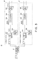
- FIGs. 3 through 6 description will be made about a switching operation from the active unit 46 to the standby unit 47 under control of the exchange system controller 25 on the assumption that a fault takes place in the active unit 46.
- input units or systems alone are illustrated for brevity of description and, as a result, an output system of each function unit 46 and 47 is omitted from Figs. 3 through 6.
- Fig. 3 it is assumed that a normal operation is carried out prior to the switching operation of the function units or systems 46 and 47. Further, it is also assumed in Fig. 3 that the function unit 46 is put into the active state and operable as the active unit or system while the function unit 47 is put into the standby state and operable as the standby unit or system, as mentioned in conjunction with Figs. 1 and 2.
- the function units 46 and 47 illustrated in Fig. 3 are labeled a current active unit and a current standby unit, respectively.
- the input data signal sequence is given to the input line accommodation unit 41 through the external input line 31 and is synchronously sent through the line accommodation unit 41 to both the current active unit 46 and the current standby unit 47.
- one of the input data signals is produced from the input line accommodation unit 41 as a first data signal that is specified by a pair of frame synchronization signals F and a communication information signal CI1 interposed between the frame synchronization signals F.
- the first data signal is followed by a second communication signal that is given to the input line accommodation unit 41 and that is specified by a communication information signal CI2 and the frame synchronization signals F.
- the first data signal is synchronously received by the input cell processors 51A and 51B.
- the input cell processor 51B in the current standby unit 47 discards the first data signal, as mentioned before. Therefore, description will be mainly directed to the current active unit 46 in connection with Fig. 3.
- the input cell processor 51A in the current active unit 46 processes the first data signal in the following manner.
- the first data signal is given to the additional information processor 511 illustrated in Fig. 2.
- the additional information processor 511 eliminates the additional information signal from the first data signal to produce an internal data signal.
- the internal data signal is temporarily memorized or stored in the local buffer 512 and is thereafter sent to the cell formation circuit 513.
- the cell formation circuit 513 converts the internal data signal into an asynchronous transfer mode (ATM) cell.
- ATM asynchronous transfer mode
- the input cell processor 51A previously produce four preceding ATM cells which precede the first data signal and which are depicted as first through fourth ATM cells C1 to C4.
- the ATM cells C1 to C4 are successively produced from the first ATM cell C1 to the fourth cell C4. This shows that the first ATM cell C1 is at first sent from the input cell processor 51A.
- the test cell insertion circuit 53A is put into an inactive state.
- the fourth ATM cell C4 is sent just before the first data signal to the input buffer 52A which is already loaded with the third cell C3 and which is sent to the test cell detector 54A.
- the test cell detector 54A produces a local reception cell as a local output cell, as exemplified by the second cell C2 in Fig. 3.
- the output cell switch 55A distributes the local output cell to the cell exchange apparatus 22 (Fig. 1) under control of the exchange controller 25. Such an operation is successively carried out as long as the current active unit 46 is operated in the normal mode.
- the communication information signal CI may be considered as a signal which has a transfer format and which has a known data communication format.
- the ATM cells converted by the input cell processor 51A depends in number on an amount of information included in the input data signal. In other words, the number of the ATM cells may not be always equal to the number of the communication information signals CI.
- the exchange system controller 25 detects a fault in the current active unit 46 and delivers, to both the current active unit 46 and the current standby unit 47, an instruction which indicates preparation of a unit switch operation and which may be called a switching preparation instruction.
- the switching preparation instruction is delivered as a control signal from the exchange system controller 25 not only to both the input cell processors 51A and 51B but also to the remaining elements of the current active unit 46 and the current standby unit 47, as illustrated in Fig. 1.
- the switching preparation instruction is assumed to be received by the both the current active unit 46 and the current standby unit 47 before the first data signal (CI1) is received by the input cell processors 51A and 51B.
- the input cell processor 51A in the current active unit 46 stops processing the input data signal and discards the input data signal which is received after reception of the switching preparation instruction.
- the illustrated input cell processor 51A converts input data signals left in the input cell processor 51B, into ATM cells, although description is made on the assumption that only one of the input data signals is left in the input cell processor 51A.
- the input data signal left in the input cell processor 51A is converted into the fourth ATM cell C4 after reception of the switching preparation instruction.
- the first data signal which includes the communication information signal CI1 is discarded or neglected by the input cell processor 51A.
- the switching preparation instruction is successively followed by an input data hold instruction which indicates a hold operation of the following data signals and a test cell insertion instruction.
- Each instruction is successively delivered from the exchange system controller 25.
- the test cell insertion circuit 53A neglects the input data hold instruction and produces a test cell TC in response to the test cell insertion instruction and sends the test cell TC to the input buffer 52A.
- the test cell TC is stored in the input buffer 52A after the fourth ATM cell C4, as shown in Fig. 4.
- the test cell detector 54A and the output cell switch 55A produce the third and the second ATM cells C3 and C2, respectively.
- the input cell processor 51B is put into an operable state in response to the switching preparation instruction produced prior to the reception of the first data signal.
- the exchange system controller 25 supplies the input cell processor 51B of the current standby unit 47 with the input data hold instruction, although the input data hold instruction is neglected by the input cell processor 51A.
- the input cell processor 51B successively stores the first data signal and the following data signals exemplified by the second data signal and a third data signal that are specified by the second communication information signal CI2 and a third communication information signal CI3 in Fig. 4, respectively.
- the exchange system controller 25 supplies the input cell processor 51B with a test cell insertion instruction simultaneously with the input cell processor 51A.
- the test cell insertion circuit 53B sends and stores the test cell TC into the input buffer 52B in synchronism with the test cell insertion instruction.
- the test cells TC are simultaneously produced by the test cell insertion circuits 53A and 53B and sent to the input buffers 52A and 52B. Consequently, the input buffer 52B is loaded with the test cell TC as a leading data signal because the input buffer 52B was empty before reception of the test cell insertion instruction, as illustrated in Fig. 4.
- test cell insertion circuits 53A and 53B supplies the exchange system controller 25 with completion signals each of which is representative of completion of inserting the test cells TC into the input buffers 54A and 54B.
- the exchange system controller 25 supplies an operation restart instruction to the current active unit 46 and the current standby unit 47. Specifically, the exchange system controller 25 instructs the input cell processor 51A of the current active unit 46 to continue a cell discard operation. Simultaneously, the exchange system controller 25 instructs the input cell processor 51B of the current standby unit 47 to carry out a cell conversion operation in connection with an input data signal already held in the input cell processor 51B and the following input data signals, such as the second and the third communication data signals CI2 and CI3.
- the input cell processor 51B of the current standby unit 47 converts the first data signal already held in the input cell processor 51B into fifth and sixth ATM cells C5 and C6 in the manner mentioned in conjunction with Fig. 2.
- the fifth and the sixth ATM cells C5 and C6 are successively stored in the input buffer 52B after the test cell TC, as illustrated in Fig. 4.
- the input buffer 52A in the current active unit 46 is loaded with the fourth ATM cell C4 which carries a last valid data signal produced before the unit switching operation while the input buffer 52B in the current standby unit 47 is loaded with ATM cells which carry valid data signal and which appear after the test cell TC.
- the test cell TC indicates a switching point from the current active unit 46 to the current standby unit 47.
- test cell (TC) detection operation which is executed after insertion of the test cell TC, as mentioned with reference to Fig. 4.
- the test cell detector 54A is at first supplied with the fourth ATM cell C4 from the input buffer 52A after the test cell TC is stored in the input buffer 52A.
- the fourth ATM cell C4 is allowed to pass through the test cell detector 54A.
- the test cell TC is sent from the input buffer 52A to the test cell detector 54A and is detected by the test cell detector 54A.
- the test cell detector 54A sends a detection signal indicative of the detection of the test cell TC to the exchange system controller 25.
- the detection signal is produced after passage of the fourth ATM cell C4.
- the input buffer 52A produces each ATM cell until detection of the test cell TC.
- the test cell detector 54B in the current standby unit 47 is at first given the test cell TC from the input buffer 52B to produce the detection signal, like the test cell detector 54A. Accordingly, the test cell TC is produced from the current standby unit 47 prior to production of the test cell TC from the current active unit 46. After production of the test cell TC from the input buffer 52B, the input buffer 52B is thereafter successively loaded with the following ATM cells, such as the fifth ATM cell C5, and so on.
- the exchange system controller 25 is supplied with the detection signal from the test cell detector 54B.
- the exchange system controller 25 sends the input buffer 52B an indication or instruction of holding and producing ATM cells, such as the fifth and the sixth ATM cells C5 and C6, and thereafter sends the test cell detector 54B an indication of discarding the test cell TC.
- the exchange system controller 25 sends the test cell detector 54A only the indication or instruction of discarding the test cell TC.
- the current active unit 46 and the current standby unit 47 are switched from one to another.
- the current active unit 46 is changed to a new standby unit while the current standby unit 47 is change to a new active unit, as illustrated in Fig. 6. Consequently, the system or unit switching operation is finished by switching both the units 46 and 47 from one to another.
- the ATM cells stored in the input buffer 52B are successively produced from the fifth ATM cell C5 and are sent through the output cell switch 55B and the system internal lines 56 to the cell exchange apparatus 22.
- the input data signals which are given to the input cell processor 51A are not converted into ATM cell and put into a standby state to be discarded by the input cell processor 51A. In consequence, none of ATM cells are sent to the following elements, such as the input buffer 52A.
- a sequence of indications or instructions is successively produced from the exchange system controller 25.
- Such indications and instructions may be, for example, the switching preparation instruction, the instruction of holding the following communication information, and the processing restart instruction. They may be delivered as the control signals to each input cell processor 51A and 51B of both the current active unit 46 and the current standby unit 47. At any rate, the control signals appear at the same timing and are synchronously delivered to both of the units 46 and 47. Using such control signals makes it possible to switch the units from one to another in a high speed communication system. In addition, if each of the input cell processors 51A and 51B can identify such a control signal during each operation, the merit is increased more and more.
- a sequence of processing operations may be automatically executed in the units 46 and 47 after reception of the switching preparation instruction sent from the exchange system controller 25.
- the system switching operation is carried out by interrupting ATM cell conversion operation of the current active unit and the current standby unit, by inserting the test cells with input data signals kept in both of the units, and by restarting the ATM cell conversion operation. Furthermore, when the test cells are detected in output stages of the current active and the current standby units 46 and 47, it is judged that the current active unit 46 finishes producing all ATM cell received prior to the system switching operation and discards the test cell. On the other hand, the ATM cells which are produced after the system switching operation are successively sent from the current standby unit.
Landscapes
- Engineering & Computer Science (AREA)
- Computer Networks & Wireless Communication (AREA)
- Signal Processing (AREA)
- Computer Security & Cryptography (AREA)
- Data Exchanges In Wide-Area Networks (AREA)
Claims (10)
- Leitungsanschlußschaltung, die mit einer Sequenz von Eingangsdatensignalen gespeist wird, um eine Sequenz von asynchronen Ausgangsübertragungsbetriebsartzellen zu einer Zellenaustauschvorrichtung zu liefern, welche Leitungsanschlußschaltung ein erstes Funktionssystem, das als aktives System betrieben wird, und ein zweites Funktionssystem aufweist, das im Aufbau identisch ist mit dem ersten Funktionssystem und als Bereitschaftssystem betrieben wird, welche Eingangsdatensignalsequenz synchron zu sowohl dem aktiven als auch dem Bereitschaftssystem gesandt wird, wobei jedes der ersten und zweiten Funktionssysteme aufweist:wobei das Bereitschaftssystem bei dem Schaltbetrieb durch den Systemcontroller so gesteuert wird, daß der Zellenprozessor im Bereitschaftssystem den Umwandlungsbetrieb beginnt, nachdem die vorbestimmte Zelle von der Zelleneinfügeschaltung zu dem Eingangspuffer im Bereitschaftssystem gesendet ist, um in dem Eingangspuffer des Bereitschaftssystems eine folgende der internen asynchronen Übertragungsbetriebsartzellen zu speichern, die der letzten der asynchronen Übertragungsbetriebsartzellen folgt, wobei der folgenden der internen asynchronen Übertragungsbetriebsartzellen die vorbestimmte Zelle im Eingangspuffer des Bereitschaftssystems vorangeht.einen Systemcontroller zum Ausführen eines Schaltbetriebes zwischen dem aktiven und dem Bereitschaftssystem, um das erste und das zweite Funktionssystem in ein neues Bereitschaftssystem und ein neues aktives System zu machen;einen steuerbaren Zellenprozessor, der durch den Systemcontroller gesteuert wird, um nacheinander unter Steuerung des Systemcontrollers einen Umwandlungsbetrieb der Eingangsdatensignale in interne asynchrone Übertragungsbetriebsartzellen durchzuführen, die den asynchronen Ausgangsübertragungsbetriebsartzellen entsprechen;eine Zelleneinfügeschaltung, die mit dem Systemcontroller verbunden ist, um unter Steuerung des Systemcontrollers eine vorbestimmte Zelle zu erzeugen, die von den internen asynchronen Übertragungsbetriebsartzellen unterschiedlich ist;einen Eingangspuffer, der mit dem Systemcontroller verbunden ist, um die internen asynchronen Übertragungsbetriebsartzellen und die vorbestimmte Zelle zu speichern, um die internen asynchronen Übertragungsbetriebsartzellen und die vorbestimmte Zelle als gespeicherte asynchrone Übertragungsbetriebsartzellen und eine gespeicherte vorbestimmte Zelle unter Steuerung durch den Systemcontroller zu speichern;einen Zellendetektor, der mit dem Systemcontroller und dem Eingangspuffer verbunden ist, um die gespeicherte vorbestimmte Zelle zu detektieren, um ein Detektionssignal an den Systemcontroller bei Detektion der gespeicherten vorbestimmten Zelle zu senden und es sonst den gespeicherten asynchronen Übertragungsbetriebsartzellen zu erlauben, unter Steuerung des Systemcontrollers hindurchzulaufen; undeine Ausgangsschaltung, die mit dem Systemcontroller und dem Zellendetektor verbunden ist, um die gespeicherten asynchronen Übertragungsbetriebsartzellen als die asynchronen Ausgangsübertragungsbetriebsartzellen unter Steuerung des Systemcontrollers zu erzeugen; welches aktive System bei dem Schaltbetrieb durch den Systemcontroller so gesteuert wird, daß der Zellenprozessor im aktiven System den Umwandlungsbetrieb während des Schaltbetriebes beendet, während die Zelleneinfügeschaltung in dem aktiven System die vorbestimmte Zelle erzeugt, nachdem wenigstens eine der internen asynchronen Übertragungsbetriebsartzellen, die in dem Zellenprozessor des aktiven Systems übrig geblieben ist, zum Eingangspuffer in dem aktiven System gesendet ist;
- Leitungsanschlußschaltung nach Anspruch 1, bei der der Eingangspuffer im aktiven System bei dem Schaltbetrieb durch den Systemcontroller so gesteuert wird, daß die letzte der internen asynchronen Übertragungsbetriebsartzellen und die vorbestimmte Zelle nacheinander ohne die folgende der internen asynchronen Übertragungsbetriebsartzellen vom Eingangspuffer im aktiven System als eine letzte der gespeicherten asynchronen Übertragungsbetriebsartzellen und die gespeicherte vorbestimmte Zelle erzeugt werden, während der Eingangspuffer im Bereitschaftssystem bei dem Schaltbetrieb so durch den Systemcontroller gesteuert wird, daß die vorbestimmte Zelle und die folgende der internen asynchronen Übertragungsbetriebsartzellen nacheinander vom Eingangspuffer in dem Bereitschaftssystem als die gespeicherte vorbestimmte Zelle und eine anfängliche der gespeicherten asynchronen Übertragungsbetriebsartzellen erzeugt werden.
- Leitungsanschlußschaltung nach Anspruch 2, bei dem der Zellendetektor im aktiven System durch den Systemcontroller beim Schaltbetrieb so gesteuert wird, daß das Detektionssignal als ein erstes Detektionssignal nach Durchgang des letzten der gespeicherten asynchronen Übertragungsbetriebsartzellen erzeugt wird, während der Zellendetektor im Bereitschaftssystem durch den Systemcontroller beim Schaltbetrieb so gesteuert wird, daß das Detektionssignal als ein zweites Detektionssignal vor der Erzeugung des ersten Detektionssignals und dem folgenden der internen asynchronen Übertragungsbetriebsartzellen erzeugt wird.
- Leitungsanschlußschaltung nach Anspruch 3, bei der der Eingangspuffer im Bereitschaftssystem durch den Systemcontroller so gesteuert wird, daß die gespeicherten asynchronen Übertragungsbetriebsartzellen erzeugt werden, nachdem sowohl das erste als auch das zweite Detektionssignal dem Systemcontroller zugeführt sind, um zu bewirken, daß das Bereitschaftssystem als das neue aktive System arbeitet und das aktive System in das neue Bereitschaftssystem umgewandelt wird.
- Systemschaltverfahren für Benutzung in einer Leitungsanschlußschaltung, der eine Sequenz von Eingangsdatensignalen zugeführt wird, um eine Sequenz von asynchronen Ausgangsübertragungsbetriebsartzellen zu einer Zellenaustauschvorrichtung zu liefern, indem ein Umwandlungsbetrieb der Eingangsdatensignale in interne asynchrone Übertragungsbetriebsartzellen durchgeführt wird, die den asynchronen Ausgangsübertragungsbetriebsartzellen entsprechen, welche Leitungsanschlußschaltung ein erstes Funktionssystem, das als aktives System betrieben wird, und ein zweites Funktionssystem aufweist, daß in seinem Aufbau identisch mit dem ersten Funktionssystem ist und als Bereitschaftssystem betrieben wird, welche Eingangsdatensignalsequenz synchron sowohl zu dem aktiven als auch zu dem Bereitschaftssystem gesendet wird, welches System Umschaltverfahren zum Durchführen eines Schaltbetriebes von dem aktiven System in das Bereitschaftssystem bestimmt ist, um das aktive und das Bereitschaftssystem in ein neues Bereitschaftssystem bzw. ein neues aktives System umzuwandeln,
welches System Schaltverfahren die Schritte aufweist:den Umwandlungsbetrieb in dem aktiven System beim Schaltbetrieb anzuhalten;in dem aktiven System eine vorbestimmte Zelle zu erzeugen, die von den internen asynchronen Übertragungsbetriebsartzellen verschieden ist und die einer letzten der internen asynchronen Übertragungsbetriebsartzellen folgt, die im aktiven System verblieben ist;nacheinander in dem aktiven System die letzte der internen asynchronen Übertragungsbetriebsartzellen und die vorbestimmte Zelle zu speichern;in dem Bereitschaftssystem die vorbestimmte Zelle synchron mit der im aktiven System erzeugten zu erzeugen;den Umwandlungsbetrieb in dem Bereitschaftssystem nach Erzeugung der vorbestimmten Zelle zu beginnen;nacheinander in dem Bereitschaftssystem die vorbestimmte Zelle und die folgende der internen asynchronen Übertragungsbetriebsartzellen zu speichern, die der letzten der internen asynchronen Übertragungsbetriebsartzellen folgt und der die vorbestimmte Zelle vorangeht. - Systemschaltverfahren nach Anspruch 5, das weiter die Schritte aufweist:nacheinander beim Schaltbetrieb im aktiven System die wenigstens eine der internen asynchronen Übertragungsbetriebsartzellen und die vorbestimmte Zelle ohne die folgende der internen asynchronen Übertragungsbetriebsartzellen zu erzeugen; undnacheinander beim Schaltbetrieb in dem Bereitschaftssystem die vorbestimmte Zelle und die folgende der internen asynchronen Übertragungsbetriebsartzellen zu erzeugen.
- Systemschaltverfahren nach Anspruch 6, das weiter die Schritte aufweist:in dem aktiven System die vorbestimmte Zelle nach Erzeugung der letzten der gespeicherten asynchronen Übertragungsbetriebsartzellen festzustellen, um ein erstes Detektionssignal zu erzeugen, das die Feststellung der vorbestimmten Zelle anzeigt;in dem Bereitschaftssystem die vorbestimmte Zelle vor dem Erzeugen der folgenden der internen asynchronen Übertragungsbetriebsartzellen zu detektieren, um ein zweites Detektionssignal zu erzeugen, das die Detektierung der vorbestimmten Zelle anzeigt.
- Systemschaltverfahren nach Anspruch 7, das weiter die Schritte aufweist:nacheinander in den Bereitschaftssystem die internen asynchronen Übertragungsbetriebsartzellen nach Erzeugung sowohl des ersten als auch des zweiten Detektionssignals herzustellen, damit das Bereitschaftssystem als das neue aktive System arbeitet;in dem aktiven System den Umwandlungsbetrieb zu beenden, um das aktive System in das neue Bereitschaftssystem umzuwandeln.
- Verfahren zum Umwandeln einer Sequenz von Dateneingangssignalen in eine Sequenz von asynchronen Übertragungsbetriebsartzellen in einer Leitungsanschlußschaltung, das es aufweist, die Eingangssignale synchron und parallel zwei funktionell identischen Umwandlungssystemen zuzuführen, von denen eines sich in einer aktiven Betriebsart und sich das andere in einer Bereitschaftsbetriebsart befindet;
die Eingangssignale in die Sequenz von Übertragungsbetriebsartzellen im aktiven System umzuwandeln;
den Betrieb des aktiven Systems zu überwachen und im Falle eines Fehlers sowohl zum aktiven als auch zum Bereitschaftssystem eine vorbestimmte Zelle zu senden, die von den Übertragungsbetriebsartzellen unterscheidbar ist;
die Umwandlung der weiteren Dateneingangssignale durch das aktive System bei Empfang der vorbestimmten Zelle durch dasselbe zu beenden und die vorbestimmte Zelle in das aktive System unmittelbar nach der letzten Übertragungsbetriebsartzelle in demselben einzusetzen;
die Umwandlung der Dateneingangssignale in Übertragungsbetriebsartzellen durch das Bereitschaftssystem bei dem Empfang der vorbestimmten Zelle durch dasselbe zu beginnen und die vorbestimmte Zelle in das Bereitschaftssystem unmittelbar vor der ersten umgewandelten Übertragungsbetriebsartzelle darin einzusetzen, wobei die erste Übertragungsbetriebsartzelle von dem Dateneingangssignal unmittelbar nach dem Dateneingangssignal umgewandelt wird, das dem Datensignal folgt, das in die letzte Übertragungsbetriebsartzelle umgewandelt ist;
die vorbestimmten Zellen in dem aktiven und dem Bereitschaftssystem zu detektieren und bei Detektierung das Bereitschaftssystem in die aktive Betriebsart und das aktive System in die Bereitschaftssystemart umzuschalten. - Leitungsanschlußschaltung, die aufweist:zwei funktionell identische Umwandlungssysteme zum Umwandeln von Dateneingangssignalen in eine Sequenz von asynchronen Übertragungsbetriebsartzellen, wobei jedes System zwischen einer aktiven Betriebsart und einer Bereitschaftsbetriebsart schaltbar ist; Mittel zum Zuführen der Dateneingangssignale synchron und parallel zu beiden Umwandlungssystemen; wobei ein System sich in der aktiven Betriebsart befindet, wenn sich das andere in der Bereitschaftsbetriebsart befindet; Mittel zum Überwachen des Betriebs des aktiven Systems und zum Senden im Falle eines Fehlers sowohl zum aktiven als auch zum Bereitschaftssystem eine vorbestimmte Zelle, die von den Übertragungsbetriebsartzellen unterscheidbar ist, wobei das aktive System so ausgebildet ist, daß es die Umwandlung von weiteren Dateneingangssignalen bei Empfang der vorbestimmten Zelle beendet unddie vorbestimmte Zelle so einsetzt, daß sie unmittelbar der letzten Übertragungsbetriebsartzelle im aktiven System folgt, wobei das Bereitschaftssystem so aufgebaut ist, daß es mit der Umwandlung der Dateneingangssignale in Übertragungsbetriebsartzellen bei Empfang der vorbestimmten Zelle beginnt, beginnend mit dem Dateneingangssignal, das unmittelbar dem Dateneingangssignal folgt, das in die letzten Übertragungsbetriebsartzelle umgewandelt ist, und um die vorbestimmte Zelle so einzusetzen, daß sie unmittelbar der ersten umgewandelten Übertragungsbetriebsartzelle im Bereitschaftssystem voran geht; Mittel zum Detektieren der vorbestimmten Zellen im aktiven und Bereitschaftssystem und Mittel, die auf die Detektion reagieren, um das aktive System in die Bereitschaftsbetriebsart und das Bereitschaftssystem in die aktive Betriebsart umzuschalten.
Applications Claiming Priority (3)
| Application Number | Priority Date | Filing Date | Title |
|---|---|---|---|
| JP35145492 | 1992-12-08 | ||
| JP35145492 | 1992-12-08 | ||
| JP351454/92 | 1992-12-08 |
Publications (3)
| Publication Number | Publication Date |
|---|---|
| EP0601853A2 EP0601853A2 (de) | 1994-06-15 |
| EP0601853A3 EP0601853A3 (en) | 1995-12-13 |
| EP0601853B1 true EP0601853B1 (de) | 2002-06-05 |
Family
ID=18417396
Family Applications (1)
| Application Number | Title | Priority Date | Filing Date |
|---|---|---|---|
| EP93309888A Expired - Lifetime EP0601853B1 (de) | 1992-12-08 | 1993-12-08 | Leitungsanschlussschaltung und Verfahren zur Vermittlungsumschaltung bei Fehlererkennung |
Country Status (4)
| Country | Link |
|---|---|
| US (1) | US5406548A (de) |
| EP (1) | EP0601853B1 (de) |
| CA (1) | CA2110864C (de) |
| DE (1) | DE69331983T2 (de) |
Families Citing this family (8)
| Publication number | Priority date | Publication date | Assignee | Title |
|---|---|---|---|---|
| JPH07250127A (ja) * | 1994-03-10 | 1995-09-26 | Fujitsu Ltd | 送信タイミング調整装置 |
| FI98595C (fi) * | 1994-07-12 | 1997-07-10 | Nokia Telecommunications Oy | Menetelmä varaprosessin lämmittämiseksi kahdennetussa reaaliaikaisessa järjestelmässä, erityisesti puhelinkeskuksessa |
| US5708684A (en) * | 1994-11-07 | 1998-01-13 | Fujitsu Limited | Radio equipment |
| US5663961A (en) * | 1995-02-24 | 1997-09-02 | Motorola, Inc. | Packet switch with centralized buffering for many output channels |
| JPH10271112A (ja) * | 1997-03-21 | 1998-10-09 | Fujitsu Ltd | 非同期転送モード交換システムにおける課金情報救済システム |
| JP3808647B2 (ja) * | 1998-12-09 | 2006-08-16 | 富士通株式会社 | セル交換モジュール、伝送装置及び伝送装置における現用・予備切り替え方法 |
| US6694373B1 (en) * | 2000-06-30 | 2004-02-17 | Cisco Technology, Inc. | Method and apparatus for hitless switchover of a voice connection in a voice processing module |
| JP3908483B2 (ja) * | 2001-06-28 | 2007-04-25 | 富士通株式会社 | 通信装置 |
Family Cites Families (4)
| Publication number | Priority date | Publication date | Assignee | Title |
|---|---|---|---|---|
| JP2677418B2 (ja) * | 1989-06-22 | 1997-11-17 | 富士通株式会社 | Atmスイッチの系切換方式 |
| GB2236930B (en) * | 1989-10-11 | 1994-03-23 | Plessey Co Plc | Method and apparatus for identifying valid cells in a redundant path combining unit of an asynchronous transfer mode switch |
| WO1991008632A1 (en) * | 1989-11-29 | 1991-06-13 | Fujitsu Limited | Changing over method for doubled atm switch system |
| JPH04290349A (ja) * | 1991-03-19 | 1992-10-14 | Fujitsu Ltd | 交換機のインサービス立ち上げ処理方式 |
-
1993
- 1993-12-07 CA CA002110864A patent/CA2110864C/en not_active Expired - Fee Related
- 1993-12-07 US US08/162,286 patent/US5406548A/en not_active Expired - Fee Related
- 1993-12-08 DE DE69331983T patent/DE69331983T2/de not_active Expired - Fee Related
- 1993-12-08 EP EP93309888A patent/EP0601853B1/de not_active Expired - Lifetime
Also Published As
| Publication number | Publication date |
|---|---|
| DE69331983T2 (de) | 2002-09-19 |
| US5406548A (en) | 1995-04-11 |
| EP0601853A3 (en) | 1995-12-13 |
| DE69331983D1 (de) | 2002-07-11 |
| CA2110864C (en) | 1999-10-05 |
| CA2110864A1 (en) | 1994-06-09 |
| EP0601853A2 (de) | 1994-06-15 |
Similar Documents
| Publication | Publication Date | Title |
|---|---|---|
| RU2635263C2 (ru) | Способ резервирования для сетей связи | |
| US5627822A (en) | Method and circuit arrangement for disturbance-free redirection of a message cell stream onto an alternate route | |
| JPH08195756A (ja) | 二重化伝送装置の回線保護切替えシステム | |
| US5315581A (en) | Hit-less protection switching method and apparatus for ATM transmission lines | |
| US8289841B2 (en) | Redundant gateway system | |
| US5406548A (en) | Line accommodation circuit capable of switching from an active system to a standby system without a loss of a communication information signal | |
| JPH04346538A (ja) | セル交換機 | |
| CA2185411C (en) | Atm cell flow control apparatus | |
| US5390163A (en) | Data exchange capable of minimizing loss of a data block | |
| US7751312B2 (en) | System and method for packet switch cards re-synchronization | |
| JP3076456B2 (ja) | 同期制御方式 | |
| US6418116B1 (en) | Transmission system having an uninterrupted switchover function for a plurality of lines | |
| JPH11313087A (ja) | 無中断伝送装置 | |
| JP3087147B2 (ja) | 同期維持制御方式 | |
| JP2806766B2 (ja) | セル入出力回線収容装置および系切替制御方法 | |
| JP3261614B2 (ja) | 信号処理システム、信号処理方法、記憶媒体 | |
| JP3189753B2 (ja) | Stm−atm変換装置の二重化方式 | |
| JPH0556065A (ja) | スイツチ同期切替方式 | |
| JPH0795213A (ja) | ディジタル交換スイッチの系切替装置 | |
| JP3110061B2 (ja) | 回線切り替え方式 | |
| JP2828140B2 (ja) | Atmスイッチ切替方式 | |
| JPH088922A (ja) | 系切り替え装置および系切り替え方法 | |
| JP2868398B2 (ja) | 伝送路切替装置 | |
| JPH06232892A (ja) | 同期制御方式 | |
| JPH05227196A (ja) | 無瞬断二重化切替え装置 |
Legal Events
| Date | Code | Title | Description |
|---|---|---|---|
| PUAI | Public reference made under article 153(3) epc to a published international application that has entered the european phase |
Free format text: ORIGINAL CODE: 0009012 |
|
| AK | Designated contracting states |
Kind code of ref document: A2 Designated state(s): DE FR GB |
|
| PUAL | Search report despatched |
Free format text: ORIGINAL CODE: 0009013 |
|
| AK | Designated contracting states |
Kind code of ref document: A3 Designated state(s): DE FR GB |
|
| 17P | Request for examination filed |
Effective date: 19951117 |
|
| GRAG | Despatch of communication of intention to grant |
Free format text: ORIGINAL CODE: EPIDOS AGRA |
|
| RTI1 | Title (correction) |
Free format text: LINE ACCOMMODATION CIRCUIT AND METHOD FOR SWITCH CHANGEOVER WHEN A FAULT IS DETECTED |
|
| RTI1 | Title (correction) |
Free format text: LINE ACCOMMODATION CIRCUIT AND METHOD FOR SWITCH CHANGEOVER WHEN A FAULT IS DETECTED |
|
| 17Q | First examination report despatched |
Effective date: 20010924 |
|
| GRAG | Despatch of communication of intention to grant |
Free format text: ORIGINAL CODE: EPIDOS AGRA |
|
| GRAH | Despatch of communication of intention to grant a patent |
Free format text: ORIGINAL CODE: EPIDOS IGRA |
|
| GRAH | Despatch of communication of intention to grant a patent |
Free format text: ORIGINAL CODE: EPIDOS IGRA |
|
| GRAA | (expected) grant |
Free format text: ORIGINAL CODE: 0009210 |
|
| AK | Designated contracting states |
Kind code of ref document: B1 Designated state(s): DE FR GB |
|
| PG25 | Lapsed in a contracting state [announced via postgrant information from national office to epo] |
Ref country code: FR Free format text: LAPSE BECAUSE OF FAILURE TO SUBMIT A TRANSLATION OF THE DESCRIPTION OR TO PAY THE FEE WITHIN THE PRESCRIBED TIME-LIMIT Effective date: 20020605 |
|
| REG | Reference to a national code |
Ref country code: GB Ref legal event code: FG4D |
|
| REF | Corresponds to: |
Ref document number: 69331983 Country of ref document: DE Date of ref document: 20020711 |
|
| PG25 | Lapsed in a contracting state [announced via postgrant information from national office to epo] |
Ref country code: GB Free format text: LAPSE BECAUSE OF NON-PAYMENT OF DUE FEES Effective date: 20021208 |
|
| EN | Fr: translation not filed | ||
| PLBE | No opposition filed within time limit |
Free format text: ORIGINAL CODE: 0009261 |
|
| STAA | Information on the status of an ep patent application or granted ep patent |
Free format text: STATUS: NO OPPOSITION FILED WITHIN TIME LIMIT |
|
| 26N | No opposition filed |
Effective date: 20030306 |
|
| PG25 | Lapsed in a contracting state [announced via postgrant information from national office to epo] |
Ref country code: DE Free format text: LAPSE BECAUSE OF NON-PAYMENT OF DUE FEES Effective date: 20030701 |
|
| GBPC | Gb: european patent ceased through non-payment of renewal fee |