EP0603168A2 - Système d'enregistrement des données numériques - Google Patents
Système d'enregistrement des données numériques Download PDFInfo
- Publication number
- EP0603168A2 EP0603168A2 EP94200371A EP94200371A EP0603168A2 EP 0603168 A2 EP0603168 A2 EP 0603168A2 EP 94200371 A EP94200371 A EP 94200371A EP 94200371 A EP94200371 A EP 94200371A EP 0603168 A2 EP0603168 A2 EP 0603168A2
- Authority
- EP
- European Patent Office
- Prior art keywords
- code
- digital data
- recording
- codes
- pulsewidth
- Prior art date
- Legal status (The legal status is an assumption and is not a legal conclusion. Google has not performed a legal analysis and makes no representation as to the accuracy of the status listed.)
- Granted
Links
- 238000000034 method Methods 0.000 claims description 13
- 230000001678 irradiating effect Effects 0.000 claims description 2
- 238000010586 diagram Methods 0.000 description 19
- 230000003287 optical effect Effects 0.000 description 10
- 238000006243 chemical reaction Methods 0.000 description 3
- 230000007423 decrease Effects 0.000 description 3
- 239000013078 crystal Substances 0.000 description 1
- 238000013500 data storage Methods 0.000 description 1
- 230000000699 topical effect Effects 0.000 description 1
Images
Classifications
-
- G—PHYSICS
- G11—INFORMATION STORAGE
- G11B—INFORMATION STORAGE BASED ON RELATIVE MOVEMENT BETWEEN RECORD CARRIER AND TRANSDUCER
- G11B20/00—Signal processing not specific to the method of recording or reproducing; Circuits therefor
- G11B20/10—Digital recording or reproducing
- G11B20/10009—Improvement or modification of read or write signals
-
- G—PHYSICS
- G11—INFORMATION STORAGE
- G11B—INFORMATION STORAGE BASED ON RELATIVE MOVEMENT BETWEEN RECORD CARRIER AND TRANSDUCER
- G11B20/00—Signal processing not specific to the method of recording or reproducing; Circuits therefor
- G11B20/10—Digital recording or reproducing
- G11B20/14—Digital recording or reproducing using self-clocking codes
- G11B20/1403—Digital recording or reproducing using self-clocking codes characterised by the use of two levels
- G11B20/1423—Code representation depending on subsequent bits, e.g. delay modulation, double density code, Miller code
- G11B20/1426—Code representation depending on subsequent bits, e.g. delay modulation, double density code, Miller code conversion to or from block codes or representations thereof
Definitions
- the present invention relates to a recording system when digital data is recorded onto a recording medium.
- RLL code Run Length Limited code
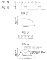
- the NRZL rule means a system in which, for instance, when the RLL coded data is as shown in Fig. 1A, this data is converted into a signal as shown in Fig. 1B.
- a recording medium generally has a reproducing characteristic such that a response of a reproduction output decreases at a high frequency as shown in Fig. 2. Therefore, when a pulse width of recording signal is narrow, the response decreases.
- the RLL codes are generally expressed as d, k, m, and n codes.
- m denotes the number of bits constituting one block of the input data series and n indicates the number of bits of one block of the input data series after completion of the conversion in the corresponding RLL code.
- d represents the minimum number of continuous code bits "0" which is permitted in the RLL codes. Namely, when d ⁇ 1, the code bit "1" does not continue.
- k indicates the maximum number of continuous code bits "0" which is permitted in the RLL code.
- Fig. 4 shows examples of a change in reproduction output in the case where a width T of recording time is large and a reproduction output in the case where it is small.
- Patent Abstracts of Japan, Vol 9, No 312 (P-411) 2035, 07.12.85 discloses an optical recording arrangement in which the pulsewidth of an original signal representing a write hole is widened in order to overcome the problem that due to the threshold level the write holes on an optical disc are reduced.
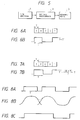
- Fig. 5 is a block diagram showing a code generator 1 for generating RLL codes and outputs the RLL codes corresponding to input data, a one shot multivibrator 2 serving as means for converting a time width T corresponding to code 1 in the RLL codes into a time width T' longer than the time width T and outputting, and recording means 3 for recording information onto a recording medium in accordance with the code having the time width T' converted.
- a magnetooptic disk apparatus for recording information onto a disk by irradiating a laser beam may be used as the recording means 3.
- Figs. 6A and 6B are explanatory diagrams of the above arrangement.
- the time width of the code 1 bit in the RLL codes is T and the codes shown in Fig. 6A are output from the code generator 1.
- the one shot multivibrator 2 converts the time width T of code 1 in the RLL codes into T' and outputs. In this case, the time width T' is longer than the time width T.
- the output of the code having the time width T' is larger than the output of the code having the time width T.
- an interval between code 1 in Fig. 6A and next code 1 is equal to an interval between the leading edge of the time width T' and the leading edge of the code of the next time width T'. Therefore, even if the time width of code 1 is changed by the multivibrator 2, the content of the information in the RLL codes does not change.
- the one shot multivibrator 2 has been shown in Fig. 5 as means for converting the time width T into the time width T', it can be also converted by another means.
- Codes shown in Fig. 7A are similar to those shown in Fig. 6A.
- T' (d + 1) x T/2 (1)
- code 1 can be easily discriminated but the width of code 0 is reduced. Therefore, there is a possibility such that the number of errors increases in the portion corresponding to code 0 due to the interference between codes.
- the density of code 1 becomes maximum in the case where d codes 0 are arranged between code 1 and the next code 1.
- the width of code 0 becomes minimum, a data error most easily occurs. Therefore, in such a case, by making the widths of codes 1 and 0 equal (duty factor 50%), the error rates of codes 1 and 0 can be equally reduced. Accordingly, it is desirable to set the time width T' as shown in the equation (1).
- the duty factor has been set to 50% only when d codes 0 are arranged between code 1 and the next code 1. However, if the duty factor is always set to 50% irrespective of the number of codes 0, the error rates of codes 1 and 0 can be always reduced. A method in this case will now be described hereinbelow.
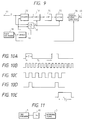
- Fig. 9 shows a practical embodiment of a time width converting method of the invention.
- Fig. 10 is a waveform diagram in each section of the circuit of Fig. 9.
- Reference numeral 11 denotes an input terminal of RLL encoded recording codes.
- a recording code waveform a shown in Fig. 10A is input to the input terminal 11.
- Reference numeral 18 denotes a clock generator of a bit rate which is twice the bit rate of the recording code.
- a crystal oscillator is used as the clock generator 18.
- Fig. 10B shows a waveform diagram of a signal which is generated from the clock generator 18.
- Reference numeral 19 denotes a 1/2 frequency divider consisting of a flip-flop circuit for frequency dividing an output of the clock generator 18 into the frequency of 1/2.
- Fig. 10C shows a waveform diagram thereof.
- Reference numeral 12 denotes a well-known counter.
- the recording code waveform is input to an enable terminal of this counter. When a low level signal is input to the enable terminal, it is counted. An output c of the frequency divider 19 is input to a count input terminal of the counter 12.
- An AND circuit 17 gets the AND of the recording code waveform a and the output c of the frequency divider 19. An output waveform of the AND circuit 17 is shown in Fig. 10D.
- a latch circuit 13 latches output data of the counter 12 in response to an output d of the AND circuit 17.
- Reference numeral 14 denotes a ROM to decide the time width T'.
- An output of the latch circuit 13 is input as an address to the ROM 14 and the data corresponding to T' is output.
- n+1 is output as an output data.
- a latch circuit 15 is similar to the latch circuit 13 and latches an output of the ROM 14.
- Reference numeral 16 denotes a well-known parallel/serial (P/S) converter consisting of a shift register or the like which uses an output of the clock generator 18 as a read clock of serial data.
- the P/S converter 16 has an output terminal 20.
- the counter 12 starts to count a clock c in response to the trailing edge of "1" of the input recording code.
- the count value of the counter 12 is latched when the signal d is generated from the AND circuit 17.
- the latched value coincides with the number of codes 0.
- T' it is sufficient to set T' as follows. Therefore, the value (n+1) which is obtained by adding "1" to the latched value is soon output from the ROM 14.
- the value (n+1) is immediately latched by the latch 15.
- An output of the latch circuit 15 is converted into a serial data train by the P/S converter 16.
- the clock to determine the reading rate of the serial output data is the output b of the clock generator 18 and its frequency is twice as high as that of the clock c of the counter 12. Therefore, the time width of the serial data read out of the P/S converter 16 is (n+1)/2. This means that this time width is compressed into 1/2 of that of the data rate of the input recording code.
- a time width pulse T' of 1/2 of the interval between the input recording codes "1" and "1" can be generated as an output of the output terminal 20.
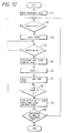
- the duty factor 50% can be also obtained by executing a program shown in a flowchart of Fig. 12.
- a CPU 30 has therein an ROM in which the program is stored, an RAM, a counter, and the like.
- the CPU 30 receives the RLL encoded recording code (step S1) and detects code 1 (step S2).
- step S3 the counter in the CPU 30 is made operative to start counting (step S3).
- step S4 and S5 The counting operation is continued until the next code 1 is detected.
- the counter counts the pulses in the CPU.
- step S6 When the next code 1 is detected, the count value of the counter at this time is fetched and the counter is reset, thereby obtaining a time width T1 between codes 1 and 1 (step S6).
- step S7 To output pulses of the time width T', a level "1" signal is output and the counting is started (step S7).
- the counting operation is continued until the time of T1/2 elapses (steps S8 and S9).
- the output of the level "1" signal is stopped and the counter is reset and the counting operation is stopped (step S9).
- the recording code of a duty factor 50% is obtained.
- the foregoing processes are repeated until the conversion of all of the input recording codes is completed (step S10).
- the recording error rate can be certainly reduced.
- the recording density can be certainly improved.
- TABLE 1 (00) 100000 (0100) 010000000000 (0101) 001000000000 (0110) 000100000000 (0111) 000010000000 (1000) 000001000000 (1001) 000000100000 (101000) 010000010000000000 (101001) 010000001000000000 (101010) 010000000100000000 (101011) 010000000010000000 (101100) 010000000001000000 (101101) 001000001000000000 (101110) 001000000100000000 (101111) 001000000010000000 (110000) 001000000001000000 (110001) 000100000100000000 (110010) 000100000010000000 (110011) 000100000001000000 (110100) 000010000010000000 (110101) 000010000001000000 (110110) 000001000001000000
Landscapes
- Engineering & Computer Science (AREA)
- Signal Processing (AREA)
- Signal Processing For Digital Recording And Reproducing (AREA)
- Optical Recording Or Reproduction (AREA)
Applications Claiming Priority (3)
| Application Number | Priority Date | Filing Date | Title |
|---|---|---|---|
| JP275079/87 | 1987-10-30 | ||
| JP62275079A JPH01118274A (ja) | 1987-10-30 | 1987-10-30 | デジタルデータの記録方式 |
| EP88310195A EP0314512B1 (fr) | 1987-10-30 | 1988-10-28 | Méthode d'enregistrement de données numériques |
Related Parent Applications (2)
| Application Number | Title | Priority Date | Filing Date |
|---|---|---|---|
| EP88310195A Division EP0314512B1 (fr) | 1987-10-30 | 1988-10-28 | Méthode d'enregistrement de données numériques |
| EP88310195.8 Division | 1988-10-28 |
Publications (3)
| Publication Number | Publication Date |
|---|---|
| EP0603168A2 true EP0603168A2 (fr) | 1994-06-22 |
| EP0603168A3 EP0603168A3 (fr) | 1994-07-20 |
| EP0603168B1 EP0603168B1 (fr) | 1999-02-03 |
Family
ID=17550523
Family Applications (2)
| Application Number | Title | Priority Date | Filing Date |
|---|---|---|---|
| EP88310195A Expired - Lifetime EP0314512B1 (fr) | 1987-10-30 | 1988-10-28 | Méthode d'enregistrement de données numériques |
| EP94200371A Expired - Lifetime EP0603168B1 (fr) | 1987-10-30 | 1988-10-28 | Meth de et système d'enregistrement des données numériques |
Family Applications Before (1)
| Application Number | Title | Priority Date | Filing Date |
|---|---|---|---|
| EP88310195A Expired - Lifetime EP0314512B1 (fr) | 1987-10-30 | 1988-10-28 | Méthode d'enregistrement de données numériques |
Country Status (4)
| Country | Link |
|---|---|
| US (1) | US5172359A (fr) |
| EP (2) | EP0314512B1 (fr) |
| JP (1) | JPH01118274A (fr) |
| DE (2) | DE3856303D1 (fr) |
Families Citing this family (7)
| Publication number | Priority date | Publication date | Assignee | Title |
|---|---|---|---|---|
| US5099237A (en) * | 1990-07-10 | 1992-03-24 | Research Corporation Technologies, Inc. | Method and apparatus for providing maximum rate modulation or compression encoding and decoding |
| JP3428039B2 (ja) * | 1992-06-30 | 2003-07-22 | ソニー株式会社 | 同期信号検出器、同期信号検出方法及び復号化装置 |
| JP3127655B2 (ja) * | 1993-03-22 | 2001-01-29 | ソニー株式会社 | 変調装置及び復調装置 |
| JP3227901B2 (ja) * | 1993-05-21 | 2001-11-12 | ソニー株式会社 | 変調方法及び復調装置 |
| JP3135753B2 (ja) * | 1993-08-26 | 2001-02-19 | キヤノン株式会社 | プローブを用いた記録再生方法および装置 |
| EP0644544B1 (fr) * | 1993-09-21 | 1999-11-17 | STMicroelectronics S.r.l. | Décodeur haute frequence avec structure en pipeline pour données à longueur de course limitée |
| DE69330957T2 (de) * | 1993-11-10 | 2002-04-04 | Stmicroelectronics S.R.L., Agrate Brianza | Programmierbarer RLL/NRZ-Dekoder für Einzel-/Doppel-Ausgangsdatenströme |
Family Cites Families (6)
| Publication number | Priority date | Publication date | Assignee | Title |
|---|---|---|---|---|
| JPS58158039A (ja) * | 1982-03-15 | 1983-09-20 | Toshiba Corp | 光ディスクの記録再生装置 |
| DE3407832C2 (de) * | 1983-03-03 | 1994-08-11 | Matsushita Electric Industrial Co Ltd | Verfahren zum Kodieren und Dekodieren binärer Daten |
| JPS60140544A (ja) * | 1983-12-28 | 1985-07-25 | Fujitsu Ltd | 光学デイスク原盤書込み装置 |
| EP0213623B1 (fr) * | 1985-09-02 | 1996-01-10 | Sharp Kabushiki Kaisha | Appareil de reproduction à disques optiques |
| JPH0656958B2 (ja) * | 1986-07-03 | 1994-07-27 | キヤノン株式会社 | 情報デ−タ復元装置 |
| EP0289004B1 (fr) * | 1987-04-28 | 1994-03-23 | Sharp Kabushiki Kaisha | Appareil d'enregistrement et de reproduction |
-
1987
- 1987-10-30 JP JP62275079A patent/JPH01118274A/ja active Pending
-
1988
- 1988-10-27 US US07/263,231 patent/US5172359A/en not_active Expired - Fee Related
- 1988-10-28 EP EP88310195A patent/EP0314512B1/fr not_active Expired - Lifetime
- 1988-10-28 DE DE3856303T patent/DE3856303D1/de not_active Expired - Lifetime
- 1988-10-28 EP EP94200371A patent/EP0603168B1/fr not_active Expired - Lifetime
- 1988-10-28 DE DE3852861T patent/DE3852861T2/de not_active Expired - Fee Related
Also Published As
| Publication number | Publication date |
|---|---|
| JPH01118274A (ja) | 1989-05-10 |
| EP0603168B1 (fr) | 1999-02-03 |
| EP0603168A3 (fr) | 1994-07-20 |
| DE3852861T2 (de) | 1995-06-08 |
| EP0314512B1 (fr) | 1995-01-25 |
| DE3852861D1 (de) | 1995-03-09 |
| EP0314512A2 (fr) | 1989-05-03 |
| DE3856303D1 (de) | 1999-03-18 |
| US5172359A (en) | 1992-12-15 |
| EP0314512A3 (en) | 1989-11-15 |
Similar Documents
| Publication | Publication Date | Title |
|---|---|---|
| US5748119A (en) | Devices and methods for channel-encoding and channel-decoding of digital data | |
| EP0605206B1 (fr) | Méthode d'enregistrement de données et appareil d'enregistrement de données | |
| US5774440A (en) | Optical data storage and retrieval system and method | |
| JP3394127B2 (ja) | ディジタルデータの伝送方法 | |
| US4833471A (en) | Data processing apparatus | |
| EP0314512B1 (fr) | Méthode d'enregistrement de données numériques | |
| US4672362A (en) | Binary data encoding and decoding process | |
| US4964139A (en) | Multi-purpose circuit for decoding binary information | |
| US6995698B2 (en) | Method and apparatus of converting a series of data words into modulated signals | |
| US5673243A (en) | Encoding unit and storage unit using the same | |
| EP0256498A2 (fr) | Compensateur d'écriture pour un appareil à disque magnétique | |
| EP0090047B1 (fr) | Systeme de codage et de decodage pour des donnees binaires | |
| US6172622B1 (en) | Demodulating device, demodulating method and supply medium | |
| JP2004518241A (ja) | 一連のmビットの情報ワードを被変調信号に変換する方法 | |
| EP0206221A2 (fr) | Appareil d'enregistrement et de reproduction pour un signal numérique | |
| EP0817180B1 (fr) | Système et procédé de stockage et d' extraction optique de données | |
| JPH02123561A (ja) | デジタルデータの記録方式 | |
| JP3239663B2 (ja) | 変調方法、変調装置及び復調装置 | |
| KR100206138B1 (ko) | 디지탈 신호 변조 방법 및 장치 | |
| JP2870060B2 (ja) | 符号化方法 | |
| JP2614206B2 (ja) | データ処理装置 | |
| JPS634270B2 (fr) | ||
| JP2705939B2 (ja) | 2進データ符号化復号化回路 | |
| JPH06111485A (ja) | 光情報記録再生装置 | |
| JPH0666696B2 (ja) | 符号化装置 |
Legal Events
| Date | Code | Title | Description |
|---|---|---|---|
| PUAI | Public reference made under article 153(3) epc to a published international application that has entered the european phase |
Free format text: ORIGINAL CODE: 0009012 |
|
| PUAL | Search report despatched |
Free format text: ORIGINAL CODE: 0009013 |
|
| AC | Divisional application: reference to earlier application |
Ref document number: 314512 Country of ref document: EP |
|
| AK | Designated contracting states |
Kind code of ref document: A2 Designated state(s): DE FR GB |
|
| AK | Designated contracting states |
Kind code of ref document: A3 Designated state(s): DE FR GB |
|
| 17P | Request for examination filed |
Effective date: 19941205 |
|
| 17Q | First examination report despatched |
Effective date: 19950420 |
|
| GRAG | Despatch of communication of intention to grant |
Free format text: ORIGINAL CODE: EPIDOS AGRA |
|
| GRAG | Despatch of communication of intention to grant |
Free format text: ORIGINAL CODE: EPIDOS AGRA |
|
| GRAG | Despatch of communication of intention to grant |
Free format text: ORIGINAL CODE: EPIDOS AGRA |
|
| GRAH | Despatch of communication of intention to grant a patent |
Free format text: ORIGINAL CODE: EPIDOS IGRA |
|
| GRAH | Despatch of communication of intention to grant a patent |
Free format text: ORIGINAL CODE: EPIDOS IGRA |
|
| GRAA | (expected) grant |
Free format text: ORIGINAL CODE: 0009210 |
|
| AC | Divisional application: reference to earlier application |
Ref document number: 314512 Country of ref document: EP |
|
| AK | Designated contracting states |
Kind code of ref document: B1 Designated state(s): DE FR GB |
|
| PG25 | Lapsed in a contracting state [announced via postgrant information from national office to epo] |
Ref country code: FR Free format text: LAPSE BECAUSE OF FAILURE TO SUBMIT A TRANSLATION OF THE DESCRIPTION OR TO PAY THE FEE WITHIN THE PRESCRIBED TIME-LIMIT Effective date: 19990203 |
|
| REF | Corresponds to: |
Ref document number: 3856303 Country of ref document: DE Date of ref document: 19990318 |
|
| PG25 | Lapsed in a contracting state [announced via postgrant information from national office to epo] |
Ref country code: DE Free format text: LAPSE BECAUSE OF FAILURE TO SUBMIT A TRANSLATION OF THE DESCRIPTION OR TO PAY THE FEE WITHIN THE PRESCRIBED TIME-LIMIT Effective date: 19990504 |
|
| EN | Fr: translation not filed | ||
| PLBE | No opposition filed within time limit |
Free format text: ORIGINAL CODE: 0009261 |
|
| STAA | Information on the status of an ep patent application or granted ep patent |
Free format text: STATUS: NO OPPOSITION FILED WITHIN TIME LIMIT |
|
| 26N | No opposition filed | ||
| REG | Reference to a national code |
Ref country code: GB Ref legal event code: IF02 |
|
| PGFP | Annual fee paid to national office [announced via postgrant information from national office to epo] |
Ref country code: GB Payment date: 20031014 Year of fee payment: 16 |
|
| PG25 | Lapsed in a contracting state [announced via postgrant information from national office to epo] |
Ref country code: GB Free format text: LAPSE BECAUSE OF NON-PAYMENT OF DUE FEES Effective date: 20041028 |
|
| GBPC | Gb: european patent ceased through non-payment of renewal fee |
Effective date: 20041028 |