EP0603899A2 - Circuit d'attaque - Google Patents
Circuit d'attaque Download PDFInfo
- Publication number
- EP0603899A2 EP0603899A2 EP93120831A EP93120831A EP0603899A2 EP 0603899 A2 EP0603899 A2 EP 0603899A2 EP 93120831 A EP93120831 A EP 93120831A EP 93120831 A EP93120831 A EP 93120831A EP 0603899 A2 EP0603899 A2 EP 0603899A2
- Authority
- EP
- European Patent Office
- Prior art keywords
- current
- output
- driver circuit
- data
- circuit
- Prior art date
- Legal status (The legal status is an assumption and is not a legal conclusion. Google has not performed a legal analysis and makes no representation as to the accuracy of the status listed.)
- Granted
Links
Images








Classifications
-
- H—ELECTRICITY
- H01—ELECTRIC ELEMENTS
- H01S—DEVICES USING THE PROCESS OF LIGHT AMPLIFICATION BY STIMULATED EMISSION OF RADIATION [LASER] TO AMPLIFY OR GENERATE LIGHT; DEVICES USING STIMULATED EMISSION OF ELECTROMAGNETIC RADIATION IN WAVE RANGES OTHER THAN OPTICAL
- H01S5/00—Semiconductor lasers
- H01S5/04—Processes or apparatus for excitation, e.g. pumping, e.g. by electron beams
- H01S5/042—Electrical excitation ; Circuits therefor
-
- H—ELECTRICITY
- H03—ELECTRONIC CIRCUITRY
- H03K—PULSE TECHNIQUE
- H03K17/00—Electronic switching or gating, i.e. not by contact-making and –breaking
- H03K17/04—Modifications for accelerating switching
- H03K17/041—Modifications for accelerating switching without feedback from the output circuit to the control circuit
- H03K17/0412—Modifications for accelerating switching without feedback from the output circuit to the control circuit by measures taken in the control circuit
- H03K17/04126—Modifications for accelerating switching without feedback from the output circuit to the control circuit by measures taken in the control circuit in bipolar transistor switches
-
- H—ELECTRICITY
- H03—ELECTRONIC CIRCUITRY
- H03K—PULSE TECHNIQUE
- H03K17/00—Electronic switching or gating, i.e. not by contact-making and –breaking
- H03K17/51—Electronic switching or gating, i.e. not by contact-making and –breaking characterised by the components used
- H03K17/56—Electronic switching or gating, i.e. not by contact-making and –breaking characterised by the components used by the use, as active elements, of semiconductor devices
- H03K17/567—Circuits characterised by the use of more than one type of semiconductor device, e.g. BIMOS, composite devices such as IGBT
-
- H—ELECTRICITY
- H03—ELECTRONIC CIRCUITRY
- H03K—PULSE TECHNIQUE
- H03K17/00—Electronic switching or gating, i.e. not by contact-making and –breaking
- H03K17/51—Electronic switching or gating, i.e. not by contact-making and –breaking characterised by the components used
- H03K17/56—Electronic switching or gating, i.e. not by contact-making and –breaking characterised by the components used by the use, as active elements, of semiconductor devices
- H03K17/60—Electronic switching or gating, i.e. not by contact-making and –breaking characterised by the components used by the use, as active elements, of semiconductor devices the devices being bipolar transistors
-
- H—ELECTRICITY
- H01—ELECTRIC ELEMENTS
- H01S—DEVICES USING THE PROCESS OF LIGHT AMPLIFICATION BY STIMULATED EMISSION OF RADIATION [LASER] TO AMPLIFY OR GENERATE LIGHT; DEVICES USING STIMULATED EMISSION OF ELECTROMAGNETIC RADIATION IN WAVE RANGES OTHER THAN OPTICAL
- H01S5/00—Semiconductor lasers
- H01S5/04—Processes or apparatus for excitation, e.g. pumping, e.g. by electron beams
- H01S5/042—Electrical excitation ; Circuits therefor
- H01S5/0428—Electrical excitation ; Circuits therefor for applying pulses to the laser
Definitions
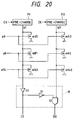
- PNP transistors 29 and 30 can be used for the current mirror circuit in the current source 12 to increase the drive capability of the current source 12. Hence the load drive capability of the driver circuit can be increased.
Landscapes
- Physics & Mathematics (AREA)
- Condensed Matter Physics & Semiconductors (AREA)
- General Physics & Mathematics (AREA)
- Electromagnetism (AREA)
- Optics & Photonics (AREA)
- Read Only Memory (AREA)
- Led Devices (AREA)
- Semiconductor Lasers (AREA)
- Semiconductor Memories (AREA)
- Light Receiving Elements (AREA)
Applications Claiming Priority (3)
| Application Number | Priority Date | Filing Date | Title |
|---|---|---|---|
| JP357742/92 | 1992-12-25 | ||
| JP35774292 | 1992-12-25 | ||
| JP35774292A JPH06196746A (ja) | 1992-12-25 | 1992-12-25 | 光電変換装置、駆動回路、半導体発光素子駆動回路、記憶装置、及びシーケンシャルアクセスメモリー |
Publications (3)
| Publication Number | Publication Date |
|---|---|
| EP0603899A2 true EP0603899A2 (fr) | 1994-06-29 |
| EP0603899A3 EP0603899A3 (fr) | 1994-10-12 |
| EP0603899B1 EP0603899B1 (fr) | 2000-09-27 |
Family
ID=18455691
Family Applications (1)
| Application Number | Title | Priority Date | Filing Date |
|---|---|---|---|
| EP93120831A Expired - Lifetime EP0603899B1 (fr) | 1992-12-25 | 1993-12-23 | Circuit d'attaque |
Country Status (4)
| Country | Link |
|---|---|
| US (1) | US5514989A (fr) |
| EP (1) | EP0603899B1 (fr) |
| JP (1) | JPH06196746A (fr) |
| DE (1) | DE69329486T2 (fr) |
Cited By (3)
| Publication number | Priority date | Publication date | Assignee | Title |
|---|---|---|---|---|
| EP0707255A1 (fr) * | 1994-10-13 | 1996-04-17 | AT&T Corp. | Circuit d'attaque pour diodes électroluminescentes composé de miroirs de courant multipliants en cascade |
| EP0924823A1 (fr) * | 1997-12-17 | 1999-06-23 | Hewlett-Packard Company | Circuit de commande pour dispositif émetteur de lumière à l'état solide |
| WO1999048206A3 (fr) * | 1998-03-18 | 2000-01-06 | Ericsson Telefon Ab L M | Circuit de commutation |
Families Citing this family (25)
| Publication number | Priority date | Publication date | Assignee | Title |
|---|---|---|---|---|
| JPH09248912A (ja) | 1996-01-11 | 1997-09-22 | Canon Inc | インクジェットヘッド及びヘッド用基体、インクジェットカートリッジ、並びにインクジェット装置 |
| US5784178A (en) * | 1996-03-06 | 1998-07-21 | Dyna Image Corporation | High performance contact image sensor |
| US5933441A (en) * | 1997-11-06 | 1999-08-03 | Chen; Hung-Ping | Circuit for protecting a laser indicator |
| JP2000012950A (ja) * | 1998-04-23 | 2000-01-14 | Matsushita Electron Corp | 半導体レ―ザ装置 |
| US6005433A (en) * | 1998-07-30 | 1999-12-21 | Credence Systems Corporation | Low charge injection mosfet switch |
| TW473984B (en) * | 1999-08-19 | 2002-01-21 | Toshiba Corp | Laser driving circuit and reproducing device using the same |
| MXPA01010039A (es) * | 2000-02-03 | 2002-07-30 | Koninkl Philips Electronics Nv | Ensamble de abastecimiento para un modulo de iluminacion led. |
| JP2001222283A (ja) * | 2000-02-09 | 2001-08-17 | Matsushita Electric Ind Co Ltd | ブザードライブ回路 |
| US6396357B1 (en) * | 2000-05-01 | 2002-05-28 | Agere Systems Guardian Corp. | Low voltage differential voltage-controlled ring oscillator |
| US6480042B2 (en) | 2000-07-04 | 2002-11-12 | Matsushita Electric Industrial Co., Ltd. | Current-to-voltage converting circuit, optical pickup head apparatus, and apparatus and method for recording/reproducing data |
| JP3835363B2 (ja) * | 2002-07-09 | 2006-10-18 | 株式会社デンソー | 車両用発電制御装置 |
| JP4017960B2 (ja) * | 2002-10-24 | 2007-12-05 | 日本テキサス・インスツルメンツ株式会社 | 駆動回路 |
| CN100352068C (zh) * | 2003-08-20 | 2007-11-28 | 沛亨半导体股份有限公司 | 以电流镜驱动发光二极管的方法 |
| CN100459821C (zh) * | 2003-11-14 | 2009-02-04 | 立锜科技股份有限公司 | 驱动多组直流光源的驱动电路 |
| JP4732243B2 (ja) | 2006-05-31 | 2011-07-27 | パナソニック株式会社 | レーザ駆動回路、光ピックアップおよび記録再生装置 |
| US7701989B2 (en) | 2006-06-05 | 2010-04-20 | Panasonic Corporation | Laser diode driving apparatus |
| JP2009094291A (ja) | 2007-10-09 | 2009-04-30 | Panasonic Corp | 光半導体装置及び赤外線データ通信装置 |
| JP5266785B2 (ja) * | 2008-02-19 | 2013-08-21 | 富士通株式会社 | 光検出装置および光検出方法 |
| US8053717B2 (en) * | 2008-05-22 | 2011-11-08 | Semiconductor Energy Laboratory Co., Ltd. | Photoelectric conversion device having a reference voltage generation circuit with a resistor and a second diode element and electronic device having the same |
| JP5491131B2 (ja) * | 2008-11-12 | 2014-05-14 | 株式会社半導体エネルギー研究所 | 光電変換装置 |
| CN105096930A (zh) * | 2014-04-30 | 2015-11-25 | 鸿富锦精密工业(武汉)有限公司 | 蜂鸣器电路 |
| US9405308B2 (en) | 2014-05-19 | 2016-08-02 | Telefonaktiebolaget Lm Ericsson (Publ) | Method and apparatus to minimize switching noise disturbance |
| JP6320273B2 (ja) * | 2014-10-27 | 2018-05-09 | 三菱電機株式会社 | 駆動回路 |
| CN108983860B (zh) * | 2018-09-18 | 2024-01-12 | 杭州洪芯微电子科技有限公司 | 基于电压校准的电流自检调节电路 |
| JP2021129259A (ja) * | 2020-02-17 | 2021-09-02 | 株式会社東芝 | 光受信回路 |
Family Cites Families (22)
| Publication number | Priority date | Publication date | Assignee | Title |
|---|---|---|---|---|
| US4121122A (en) * | 1976-12-22 | 1978-10-17 | Kurt Pokrandt | Current sensing circuitry |
| US4221979A (en) * | 1977-12-08 | 1980-09-09 | Rca Corporation | Non-inverting buffer circuits |
| JPS56156993A (en) * | 1980-05-08 | 1981-12-03 | Fujitsu Ltd | Read only memory |
| US4295226A (en) * | 1980-07-02 | 1981-10-13 | Bell Telephone Laboratories, Incorporated | High speed driver for optoelectronic devices |
| JPS5762779A (en) * | 1980-09-29 | 1982-04-15 | Toshiba Corp | Alwave rectifying circuit |
| JPS5766324A (en) * | 1980-10-13 | 1982-04-22 | Sharp Corp | Light receiving circuit |
| JPS5855582B2 (ja) * | 1981-11-13 | 1983-12-10 | 株式会社東芝 | 透視性テ−プカセツト |
| US4634902A (en) * | 1982-11-17 | 1987-01-06 | Clarion Co., Ltd. | Circuit arrangement capable of adjusting a threshold level of a differential transistor circuit |
| US4544878A (en) * | 1983-10-04 | 1985-10-01 | At&T Bell Laboratories | Switched current mirror |
| JPS60128711A (ja) * | 1983-12-15 | 1985-07-09 | Fujitsu Ltd | トランジスタ切替回路 |
| JPS61108931A (ja) * | 1984-10-31 | 1986-05-27 | Ricoh Co Ltd | 光量測定方法 |
| DE3604971A1 (de) * | 1986-02-17 | 1987-08-20 | Messerschmitt Boelkow Blohm | Photosensoreinrichtung mit dunkelstromkompensation |
| DE3705915C2 (de) * | 1987-02-25 | 1996-09-05 | Sel Alcatel Ag | Schaltungsanordnung zur Differenzbildung zweier Photoströme |
| US4831395A (en) * | 1987-04-01 | 1989-05-16 | Eastman Kodak Company | Printer apparatus |
| US4916307A (en) * | 1987-12-15 | 1990-04-10 | Fuji Electric Co., Ltd. | Light intensity detecting circuit with dark current compensation |
| US4812907A (en) * | 1987-12-31 | 1989-03-14 | Zenith Electronics Corporation | Sync pulse separator system |
| DE68921020T2 (de) * | 1988-05-20 | 1995-06-29 | Mitsubishi Electric Corp | Integrierte MOS-Schaltung zum Steuern von lichtermittierenden Dioden. |
| US5117099A (en) * | 1989-09-01 | 1992-05-26 | Schmidt Terrence C | Ambient light rejecting quad photodiode sensor |
| KR930000815B1 (ko) * | 1990-02-20 | 1993-02-05 | 삼성전자 주식회사 | Rom 회로 |
| US5130923A (en) * | 1990-06-06 | 1992-07-14 | Valitek, Inc. | Selective dynamic RAM address generator with provision for automatic refresh |
| JPH04117007A (ja) * | 1990-08-31 | 1992-04-17 | Fuji Electric Co Ltd | 多出力定電流駆動回路 |
| US5212456A (en) * | 1991-09-03 | 1993-05-18 | Allegro Microsystems, Inc. | Wide-dynamic-range amplifier with a charge-pump load and energizing circuit |
-
1992
- 1992-12-25 JP JP35774292A patent/JPH06196746A/ja active Pending
-
1993
- 1993-12-21 US US08/170,753 patent/US5514989A/en not_active Expired - Fee Related
- 1993-12-23 DE DE69329486T patent/DE69329486T2/de not_active Expired - Fee Related
- 1993-12-23 EP EP93120831A patent/EP0603899B1/fr not_active Expired - Lifetime
Cited By (5)
| Publication number | Priority date | Publication date | Assignee | Title |
|---|---|---|---|---|
| EP0707255A1 (fr) * | 1994-10-13 | 1996-04-17 | AT&T Corp. | Circuit d'attaque pour diodes électroluminescentes composé de miroirs de courant multipliants en cascade |
| EP0924823A1 (fr) * | 1997-12-17 | 1999-06-23 | Hewlett-Packard Company | Circuit de commande pour dispositif émetteur de lumière à l'état solide |
| US6028871A (en) * | 1997-12-17 | 2000-02-22 | Hewlett-Packard Company | Driver circuit for a solid state optical emitter device |
| WO1999048206A3 (fr) * | 1998-03-18 | 2000-01-06 | Ericsson Telefon Ab L M | Circuit de commutation |
| US6288660B1 (en) | 1998-03-18 | 2001-09-11 | Telefonaktiebolaget Lm Ericsson | BiCMOS circuit for controlling a bipolar current source |
Also Published As
| Publication number | Publication date |
|---|---|
| JPH06196746A (ja) | 1994-07-15 |
| EP0603899A3 (fr) | 1994-10-12 |
| EP0603899B1 (fr) | 2000-09-27 |
| US5514989A (en) | 1996-05-07 |
| DE69329486T2 (de) | 2001-05-10 |
| DE69329486D1 (de) | 2000-11-02 |
Similar Documents
| Publication | Publication Date | Title |
|---|---|---|
| US5514989A (en) | Semiconductor light emitting element driver circuit | |
| US5740102A (en) | Data retention circuit and semiconductor memory device using the same | |
| JP3754593B2 (ja) | データビットを記憶するメモリーセルを有する集積回路および集積回路において書き込みデータビットをメモリーセルに書き込む方法 | |
| JPS6161198B2 (fr) | ||
| JP2696864B2 (ja) | メモリ装置 | |
| KR950001289B1 (ko) | 반도체기억장치 | |
| JPH09204775A (ja) | 半導体集積回路装置 | |
| EP0591650A2 (fr) | Mémoire ayant un amplificateur verrouilleur de détection BICMOS | |
| JP3110113B2 (ja) | スタティック型メモリ | |
| JP2662822B2 (ja) | 半導体記憶装置 | |
| IE52821B1 (en) | Static memory circuit | |
| US6307793B1 (en) | Memory device, coupling noise eliminator, and coupling noise elimination method | |
| US5229966A (en) | Current control circuit for dynamic memory | |
| US4435789A (en) | Circuit for a read-only memory organized in rows and columns to prevent bit line potentials from dropping | |
| TW297899B (en) | Dynamic random access memory array | |
| US7301840B2 (en) | Semiconductor memory device | |
| KR950005516B1 (ko) | 이중포트형 반도체 집적기억회로 | |
| US5444660A (en) | Sequential access memory and its operation method | |
| JPH03263684A (ja) | ダイナミック・ランダム・アクセス・メモリ | |
| KR950014090B1 (ko) | 비휘발성 메모리장치의 센스회로 | |
| EP0262413A1 (fr) | Dispositif de mémoire à multiplexage d'adresses | |
| JPH0722939A (ja) | 論理回路 | |
| JPH11250670A (ja) | 半導体記憶装置 | |
| JP7799593B2 (ja) | 半導体記憶装置 | |
| EP0520450A2 (fr) | Mémoire à semi-conducteur |
Legal Events
| Date | Code | Title | Description |
|---|---|---|---|
| PUAI | Public reference made under article 153(3) epc to a published international application that has entered the european phase |
Free format text: ORIGINAL CODE: 0009012 |
|
| AK | Designated contracting states |
Kind code of ref document: A2 Designated state(s): DE FR GB IT NL |
|
| PUAL | Search report despatched |
Free format text: ORIGINAL CODE: 0009013 |
|
| AK | Designated contracting states |
Kind code of ref document: A3 Designated state(s): DE FR GB IT NL |
|
| 17P | Request for examination filed |
Effective date: 19950227 |
|
| 17Q | First examination report despatched |
Effective date: 19970124 |
|
| GRAG | Despatch of communication of intention to grant |
Free format text: ORIGINAL CODE: EPIDOS AGRA |
|
| GRAG | Despatch of communication of intention to grant |
Free format text: ORIGINAL CODE: EPIDOS AGRA |
|
| GRAH | Despatch of communication of intention to grant a patent |
Free format text: ORIGINAL CODE: EPIDOS IGRA |
|
| GRAH | Despatch of communication of intention to grant a patent |
Free format text: ORIGINAL CODE: EPIDOS IGRA |
|
| GRAA | (expected) grant |
Free format text: ORIGINAL CODE: 0009210 |
|
| AK | Designated contracting states |
Kind code of ref document: B1 Designated state(s): DE FR GB IT NL |
|
| REF | Corresponds to: |
Ref document number: 69329486 Country of ref document: DE Date of ref document: 20001102 |
|
| ITF | It: translation for a ep patent filed | ||
| ET | Fr: translation filed | ||
| PLBE | No opposition filed within time limit |
Free format text: ORIGINAL CODE: 0009261 |
|
| STAA | Information on the status of an ep patent application or granted ep patent |
Free format text: STATUS: NO OPPOSITION FILED WITHIN TIME LIMIT |
|
| 26N | No opposition filed | ||
| REG | Reference to a national code |
Ref country code: GB Ref legal event code: IF02 |
|
| PGFP | Annual fee paid to national office [announced via postgrant information from national office to epo] |
Ref country code: FR Payment date: 20021210 Year of fee payment: 10 |
|
| PGFP | Annual fee paid to national office [announced via postgrant information from national office to epo] |
Ref country code: GB Payment date: 20021218 Year of fee payment: 10 |
|
| PGFP | Annual fee paid to national office [announced via postgrant information from national office to epo] |
Ref country code: NL Payment date: 20021227 Year of fee payment: 10 |
|
| PGFP | Annual fee paid to national office [announced via postgrant information from national office to epo] |
Ref country code: DE Payment date: 20021231 Year of fee payment: 10 |
|
| PG25 | Lapsed in a contracting state [announced via postgrant information from national office to epo] |
Ref country code: GB Free format text: LAPSE BECAUSE OF NON-PAYMENT OF DUE FEES Effective date: 20031223 |
|
| PG25 | Lapsed in a contracting state [announced via postgrant information from national office to epo] |
Ref country code: NL Free format text: LAPSE BECAUSE OF NON-PAYMENT OF DUE FEES Effective date: 20040701 Ref country code: DE Free format text: LAPSE BECAUSE OF NON-PAYMENT OF DUE FEES Effective date: 20040701 |
|
| GBPC | Gb: european patent ceased through non-payment of renewal fee |
Effective date: 20031223 |
|
| PG25 | Lapsed in a contracting state [announced via postgrant information from national office to epo] |
Ref country code: FR Free format text: LAPSE BECAUSE OF NON-PAYMENT OF DUE FEES Effective date: 20040831 |
|
| NLV4 | Nl: lapsed or anulled due to non-payment of the annual fee |
Effective date: 20040701 |
|
| REG | Reference to a national code |
Ref country code: FR Ref legal event code: ST |
|
| PG25 | Lapsed in a contracting state [announced via postgrant information from national office to epo] |
Ref country code: IT Free format text: LAPSE BECAUSE OF NON-PAYMENT OF DUE FEES Effective date: 20051223 |