EP0604048A2 - Asynchroner, digitaler Schwellwertdetektor für einen digitalen Datenspeicherkanal - Google Patents
Asynchroner, digitaler Schwellwertdetektor für einen digitalen Datenspeicherkanal Download PDFInfo
- Publication number
- EP0604048A2 EP0604048A2 EP93309709A EP93309709A EP0604048A2 EP 0604048 A2 EP0604048 A2 EP 0604048A2 EP 93309709 A EP93309709 A EP 93309709A EP 93309709 A EP93309709 A EP 93309709A EP 0604048 A2 EP0604048 A2 EP 0604048A2
- Authority
- EP
- European Patent Office
- Prior art keywords
- signal
- digital
- threshold
- digital signals
- data
- Prior art date
- Legal status (The legal status is an assumption and is not a legal conclusion. Google has not performed a legal analysis and makes no representation as to the accuracy of the status listed.)
- Withdrawn
Links
- 238000013500 data storage Methods 0.000 title claims description 5
- 230000007704 transition Effects 0.000 claims abstract description 51
- 238000001514 detection method Methods 0.000 claims abstract description 40
- 238000005070 sampling Methods 0.000 claims description 44
- 238000000034 method Methods 0.000 claims description 15
- 238000012797 qualification Methods 0.000 claims description 12
- 230000003287 optical effect Effects 0.000 claims description 9
- 238000012546 transfer Methods 0.000 claims description 2
- 230000009977 dual effect Effects 0.000 claims 1
- 230000003111 delayed effect Effects 0.000 description 6
- 230000001360 synchronised effect Effects 0.000 description 6
- 238000010586 diagram Methods 0.000 description 4
- 238000012545 processing Methods 0.000 description 4
- 230000004069 differentiation Effects 0.000 description 3
- 230000008859 change Effects 0.000 description 2
- 238000006243 chemical reaction Methods 0.000 description 2
- 238000012986 modification Methods 0.000 description 2
- 230000004048 modification Effects 0.000 description 2
- 238000004590 computer program Methods 0.000 description 1
- 238000011156 evaluation Methods 0.000 description 1
- 238000001914 filtration Methods 0.000 description 1
- 230000036039 immunity Effects 0.000 description 1
- 238000013139 quantization Methods 0.000 description 1
- 238000004088 simulation Methods 0.000 description 1
Images


Classifications
-
- H—ELECTRICITY
- H03—ELECTRONIC CIRCUITRY
- H03K—PULSE TECHNIQUE
- H03K5/00—Manipulating of pulses not covered by one of the other main groups of this subclass
- H03K5/153—Arrangements in which a pulse is delivered at the instant when a predetermined characteristic of an input signal is present or at a fixed time interval after this instant
- H03K5/1536—Zero-crossing detectors
-
- G—PHYSICS
- G11—INFORMATION STORAGE
- G11B—INFORMATION STORAGE BASED ON RELATIVE MOVEMENT BETWEEN RECORD CARRIER AND TRANSDUCER
- G11B20/00—Signal processing not specific to the method of recording or reproducing; Circuits therefor
- G11B20/10—Digital recording or reproducing
- G11B20/10009—Improvement or modification of read or write signals
Definitions
- the present invention relates to zero-crossing threshold detectors in general and, more specifically, to a digital Zero-crossing detector for providing a digital output signal representing the detection location within an asynchronous sampling window.
- binary data is encoded and stored on optical or magnetic media as a series of optical or magnetic transitions.
- Retrieval of stored data requires a detecting and decoding system in the recording channel to reconstruct the original binary data and synchronous clock from the self-clocking analog signal waveform created by the magnetic or optical transducer adjacent to the storage medium.
- Practitioners in the art have proposed many solutions to the problems associated with extracting synchronous clock and data from a self-clocking data signal. These problems include discrimination between actual transitions and mere noise pulses and precise reconstruction of the synchronous data clock signal to permit accurate decoding of the phase-encoded data.
- An important element in such recording channels is the waveform transition or "zero-crossing" detector, which is necessary to accurately determine the precise relative timing or phase of each self-clocking waveform transition.
- Analog pulse detectors known in the art suffer from the usual disadvantages of analog electronic apparatus. They are expensive, bulky and subject to calibration drift over time. Moreover, analog pulse detectors are generally suited to a narrow predetermined range of channel data rates, imposing severe channel data rate restrictions on storage media data retrieval systems. Digital implementations of data pulse or transition phase detectors known in the art usually rely on discrete-signal embodiments of the well-known analog detection techniques. For instance, the analog signal waveform is first sampled and digitized using well-known Phase-Locked Loop (PLL) techniques. These samples are then processed digitally to remove unwanted frequency components and to reconstruct the synchronous clock and data.
- PLL Phase-Locked Loop
- Digital computer programs are known in the art for simulating the functions of analog recording channels but these techniques require high sampling rates, making implementation in real-time hardware expensive and difficult.
- Some of the difficulty involved in digital implementation can be overcome by reducing the asynchronous analog signal sampling rate.
- a reduced asynchronous sampling rate results in increased uncertainty of the zero-crossing detection time. This leads to jitter distortion and increased Bit Error Rate (BER) in the recording channel.
- BER Bit Error Rate
- an Asynchronous Digital Threshold Detector for detecting the time t of a threshold transition in a signal waveform having a data clock rate F d
- a zero-crossing threshold detector designed for use in an asynchronous digital channel. It receives a digitized signal waveform in which self-clocking data is encoded and outputs the relative location of a zero-crossing within the sample period, if any.
- This digital output which is intended for use in recovering the embedded data and clock signals, is in a digital form that can be used directly by the Discrete Time Control Loop (DTCL) disclosed in a copending US patent application No 07/967,588 by R.A. Hutchins et al entitled "Discrete Time Control Loop Method And Apparatus For Clocking Data In An Asynchronous Channel", which is included herein in its entirety by this reference.
- DTCL Discrete Time Control Loop
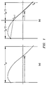
- the Asynchronous Digital Threshold Detector (ADTD) of this invention employs the following three steps to estimate the zero-crossing arrival time within a single sampling interval. First, the detector determines if a zero-crossing has occurred by examining adjacent sample pairs for changes in sign. Secondly, the sample rate is converted from the higher sampling rate to a lower sampling rate, which is exactly half of the higher rate. In doing this, the ADTD first determines which half of the new longer sample period contains the zero-crossing. Finally, the ADTD determines the subcell time estimate; that is, the proportional location of the zero-crossing within the shorter sampling period by solving a linear interpolation formula (Fig. 1 (b)). The detector output is an n-bit digital signal representing the estimated fraction of time elapsed within the longer sampling interval at the zero-crossing point (t/T d in Fig. 1 (a)).
- the present invention advantageously improves zero-crossing accuracy at lower asynchronous sampling rates.
- the present invention further advantageously permits threshold crossings to be detected in a stream of digital samples without recourse to analog components.
- the zero-crossing detections are presented in the form of an n-bit digital word, the accuracy of which is independent of analog signal timing considerations.
- the ADTD of this invention determines the subcell time estimate t ⁇ (Fig. 1 (b)) and converts it to a digital representation of the ratio t/T d (Fig. 1 (a)).
- Fig. 2 illustrates the relationship between the ADTD 10 of the present invention and the optical or magnetic data storage medium 12.
- a peak detection channel implementation is shown for illustrative purposes.
- Magnetic or optical transitions in medium 12 are sensed by a transducer 14 in any useful manner known in the art.
- the transducer output signal 16 is presented to the usual analog functions 18. These functions include preamplification, Automatic Gain Control (AGC), and anti-aliasing (low-pass) filtering.
- AGC Automatic Gain Control
- A/D Analog-to-Digital
- the digital sample signals ⁇ S ⁇ are forwarded on a sample bus 28 to ADTD 10.
- the pulse qualifier 30 generates a pulse qualification flag that is forwarded on a line 32 to ADTD 10.
- the pulse qualification flag discriminates between signal pulses and noise pulses in any useful manner known in the art and is asserted during every sample interval T s containing a qualified pulse or transition.
- the ADTD embodiment 10 in Fig. 2 embraces a pulse detector 34, a 2x-to-1x converter 36 and a time generator 38.
- ADTD 10 provides two digital outputs.
- a digital signal representing the relative position of a threshold transition within a data clock interval (t/T d ) is provided on a data bus 40 and a Pulse Detection Flag (PDF) is forwarded on a line 42.
- Line 42 is high during the entire data clock interval T d that contains a qualified threshold transition detection.
- Fig. 2 shows bus 40 and line 42 feeding into a Discrete Time Control Loop (DTCL) 44 for subsequent read-back channel processing in accordance with the above-cited Hutchins et al patent application.
- DTCL Discrete Time Control Loop
- Any other suitable methods may also be employed to extract data and synchronous clock signals from ADTD 10 digital outputs on bus 40 and line 42, such as digital-to-analog conversion followed by phase-locked loop signal processing.
- a signal differentiator 46 differentiates data signal waveform 20 to convert waveform peaks to zero-crossing transitions in any useful manner known to the art.
- medium 12 consists of the magnetic tape in a tape drive 48 or the magnetic disk surface in a Direct Access Storage Device (DASD) 50
- the data recovered appear in waveform 20 as peaks or pulses. Detection of such pulses requires differentiation in signal differentiator 46.
- the signal may be Pulse-Width-Modulated (PWM) so that the recovered data are encoded as waveform transitions through a variable but predetermined threshold.
- PWM Pulse-Width-Modulated
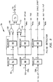
- pulse detector 34 must actually detect signal waveform transitions through zero. In operation, pulse detector 34 can be better understood with reference to Fig. 3.
- the pulse qualification flag on line 32 is stored in register 54.
- a register 56 stores a once-delayed value for the pulse qualification flag and an OR-gate 58 provides an enabling qualification flag on line 60 that is asserted if there is a qualified detection in either the present (i) th or the immediately preceding (i-1) th sampling interval T s .
- the digital signal on bus 28 is split into the sign bit at a line 28a and the remaining 7-bit mantissa on a bus 28b.
- the registers 66 and 68 store the sign of the present sample S i and the sign of the immediately preceding sample S i-1 for comparison.
- An XOR-gate 70 provide a detection flag on line 72 that is high whenever there is a change in sign between S i-1 and S i .
- An AND-gate 74 combines the enabling qualification flag on line 60 and the transition detection flag on line 72 to provide a detection flag DF i at an output line 76.
- the 7-bit registers 78 and 80 serve to assemble pairs of digital signals (y k-1 , y k ) that represent adjacent sample pairs (S i-1 , S i ).
- the present digital signal y k is passed through on the bus 82 (with its sign carried on line 82a) and the once-delayed digital signal y k-1 is passed through on the bus 86 (with its sign on line 86a).
- Buses 82 and 86 and flag line 76 carry the adjacent digital signal pair and the associated detection flag to converter 36 (Fig. 2).
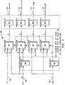
- Converter 36 can he better understood with reference to Fig. 4.
- Converter 36 acts as a "decimator", which replaces a digital signal pair with a single digital signal.
- the input registers 90 and 92 are clocked at the sample clock rate F s .
- Register 90 stores the delayed signal value y k-1 .
- Register 92 stores the DF i detection flag, which flags a detection within the present T s interval.
- the present signal y k on bus 82 is presented directly to the first input of a multiplexer 94. Delayed signal y k-1 is presented to the second input of multiplexer 94 and to the first input of another multiplexer 96.
- the second input of multiplexer 96 is provided with y k-2 , which is merely y k-1 delayed by one additional sampling clock interval T s .
- the two multiplexers 98 and 100 are provided with detection flag DF i at their first inputs and a fixed binary "0" or "1" at their second inputs as shown in Fig. 4. Accordingly, as detection flag DF i is clocked through register 92 by the sampling clock F s , the inputs to multiplexers 94-100 are passed through to registers 102, 104, 106 and 108. Registers 102-108 are clocked at half the rate of registers 90-92.
- converter 36 selects the adjacent digital signals and the detection flag in the subcell where the zero-crossing occurs (it is assumed that a maximum of one zero-crossing can occur per nominal sample period).
- Converter 36 also holds the present digital signal y k on bus 110 and the once-delayed digital signal y k-1 on bus 112 to represent a qualified adjacent sample pair (S i-1 , S i ). This pair is held for two T s sample intervals and is forwarded to time generator 38 for additional processing.
- MSB Most Significant Bit
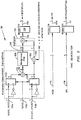
- Fig. 5 shows a detailed embodiment of time generator 38.
- the purpose of generator 38 is to estimate the zero-crossing arrival time by solving an interpolation equation relating the transition detection to the digital signals (y k-1 , y k ) representing adjacent sample pair (S i-1 , S i ) preserved in registers 102 and 104 (Fig. 4). This pair is input to generator 38 on the buses 110 and 112.
- the 8-bit digital signal on bus 110 is split, with the MSB on line 110b and the remaining 7-bit mantissa on bus 110a in Fig. 5.
- the seven LSBs are provided at bus 112b in Fig. 5.
- the MSB from bus 112 (Fig. 4) is unnecessary, being implied by the combination of DF i on line 116 and the sign bit at line 110b.
- a preferred formula is a simple linear interpolation equation: where y k is the intermediate digital signal equivalent to sample S i .
- y k is the intermediate digital signal equivalent to sample S i .
- the sign of y k is the opposite of y k-1 , permitting the above equation to be rewritten as This simplifies the evaluation of the earlier interpolation equation by eliminating the sign bit.
- is first determined at the denominator signal bus 118. This is accomplished by the multiplexers 120 and 122 and the summer 124 as follows. Multiplexer 120 selects the absolute value of the present signal y k and multiplexer 122 selects the absolute value of the delayed signal y k-1 when y k has a positive sign at line 110b. If the sign of Y k is negative, the 2s-compliments of these two digital signals are selected. Summer 124 adds the two selected 7-bit digital signals to provide the denominator signal
- Denominator signal 118 is then inverted by any useful means, such as by a reciprocal map 126.
- Map 126 operates in any useful manner known in the art, such as a 256-Byte lookup table, and provides a 12-bit output reciprocal signal on a bus 128.
- a summer 130 modifies the delayed digital signal y k-1 that was selected in multiplexer 122, depending on the sign bit of the delayed signal y k-1 , and produces the absolute value of
- a multiplier 134 multiplies the 12-bit reciprocal output signal on bus 128 with the 7-bit numerator on bus 132 and strips the 14 LSBs from the result, leaving a 5-bit zero-crossing signal on bus 136.
- This signal is then stored for one sample interval in register 138 to provide the additional delay necessary to synchronize operation with the remainder of generator 38.
- the output zero-crossing estimate signal t/T d is provided on bus 40, with the MSB at line 40a signifying which of two adjacent sampling periods T s contains the event.
- Figs. 2-5 The preferred embodiment disclosed in Figs. 2-5 has been tested, using an 8-bit input sample on bus 28, a tracking threshold bit that indicates whether the given sample is over a qualification threshold on line 32 and outputting a 6-bit time estimate on bus 40 with a valid sample flag (PDF) on line 42.
- PDF valid sample flag
- ADTD 10 requires approximately 1500 gates.
- the preferred embodiment has also been implemented in a magnetic tape data storage system.
- y k was fixed at 0.5 and y k-1 was varied across the full range of possible values (all ranges were normalized to unity). The simulated results are very closely aligned with the theoretical results.
- y k-1 was fixed at 0.5 and y k was varied across the full range of possible values.
- the simulated ADTD 10 performance closely matches the expected output across the full range of possible inputs. The differences between the two curves in each of Figs. 6a and 6b result from quantization error.
Landscapes
- Engineering & Computer Science (AREA)
- Signal Processing (AREA)
- Physics & Mathematics (AREA)
- Nonlinear Science (AREA)
- Signal Processing For Digital Recording And Reproducing (AREA)
Applications Claiming Priority (4)
| Application Number | Priority Date | Filing Date | Title |
|---|---|---|---|
| US99584992A | 1992-12-23 | 1992-12-23 | |
| US73921 | 1993-06-07 | ||
| US08/073,921 US5315284A (en) | 1992-12-23 | 1993-06-07 | Asynchronous digital threshold detector for a digital data storage channel |
| US995849 | 1993-06-07 |
Publications (2)
| Publication Number | Publication Date |
|---|---|
| EP0604048A2 true EP0604048A2 (de) | 1994-06-29 |
| EP0604048A3 EP0604048A3 (de) | 1995-11-08 |
Family
ID=26755040
Family Applications (1)
| Application Number | Title | Priority Date | Filing Date |
|---|---|---|---|
| EP93309709A Withdrawn EP0604048A3 (de) | 1992-12-23 | 1993-12-03 | Asynchroner, digitaler Schwellwertdetektor für einen digitalen Datenspeicherkanal. |
Country Status (3)
| Country | Link |
|---|---|
| US (1) | US5315284A (de) |
| EP (1) | EP0604048A3 (de) |
| JP (1) | JP2802027B2 (de) |
Cited By (1)
| Publication number | Priority date | Publication date | Assignee | Title |
|---|---|---|---|---|
| WO2004090892A1 (en) * | 2003-04-07 | 2004-10-21 | Koninklijke Philips Electronics N.V. | Cross-talk cancellation scheme for rll-based storage systems |
Families Citing this family (18)
| Publication number | Priority date | Publication date | Assignee | Title |
|---|---|---|---|---|
| KR100303703B1 (ko) * | 1993-03-10 | 2001-11-22 | 클라크 3세 존 엠. | 자기조정한계를지니는데이타신호비교기 |
| US5453714A (en) * | 1993-03-10 | 1995-09-26 | National Semiconductor Corporation | Binary FM demodulator with self-adjusting resonant operating frequency according to demodulated binary output signal duty cycle |
| US5530601A (en) * | 1993-09-30 | 1996-06-25 | International Business Machines Corporation | Tracking threshold circuit for peak detection |
| US5396479A (en) * | 1994-05-06 | 1995-03-07 | Maxoptix Corporation | Apparatus and method for setting a threshold level to maintain duty cycle in a pulse width modulated optical recording system |
| US5696639A (en) * | 1995-05-12 | 1997-12-09 | Cirrus Logic, Inc. | Sampled amplitude read channel employing interpolated timing recovery |
| US5717619A (en) * | 1995-10-20 | 1998-02-10 | Cirrus Logic, Inc. | Cost reduced time varying fir filter |
| US5760984A (en) * | 1995-10-20 | 1998-06-02 | Cirrus Logic, Inc. | Cost reduced interpolated timing recovery in a sampled amplitude read channel |
| US5726818A (en) * | 1995-12-05 | 1998-03-10 | Cirrus Logic, Inc. | Magnetic disk sampled amplitude read channel employing interpolated timing recovery for synchronous detection of embedded servo data |
| US5812336A (en) * | 1995-12-05 | 1998-09-22 | Cirrus Logic, Inc. | Fixed sample rate sampled amplitude read channel for zoned magnetic recording |
| US6819514B1 (en) | 1996-04-30 | 2004-11-16 | Cirrus Logic, Inc. | Adaptive equalization and interpolated timing recovery in a sampled amplitude read channel for magnetic recording |
| US5825744A (en) * | 1996-05-13 | 1998-10-20 | International Business Machines Corporation | Configurable read detection channel and method for decoding data stored within a data storage medium |
| US6317469B1 (en) | 1996-06-28 | 2001-11-13 | Lsi Logic Corporation | Method and apparatus for utilizing a data processing system for multi-level data communications providing self-clocking |
| US5802118A (en) * | 1996-07-29 | 1998-09-01 | Cirrus Logic, Inc. | Sub-sampled discrete time read channel for computer storage systems |
| US5877644A (en) * | 1997-01-08 | 1999-03-02 | International Business Machines Corporation | Programmable digital envelope following threshold generation apparatus and method |
| US6278747B1 (en) | 1998-03-13 | 2001-08-21 | International Business Machines Corporation | Method and apparatus for performing digital detection of data stored on an optical medium |
| US6385260B1 (en) | 1998-09-25 | 2002-05-07 | Hewlett-Packard Company | Asynchronous sampling digital detection (ASDD) methods and apparatus |
| US6662321B1 (en) * | 2000-03-21 | 2003-12-09 | Conexant Systems, Inc. | Modem using phase coherence to adapt for missing transmission samples |
| US7839317B1 (en) | 2009-07-13 | 2010-11-23 | Don Roy Sauer | Folding comparator compatible with level-crossing sampling |
Family Cites Families (21)
| Publication number | Priority date | Publication date | Assignee | Title |
|---|---|---|---|---|
| US3593166A (en) * | 1969-12-17 | 1971-07-13 | Bell Telephone Labor Inc | Zero crossing detector |
| US3840753A (en) * | 1972-10-02 | 1974-10-08 | Texas Instruments Inc | Tape read amplifier and logic circuit |
| US3955102A (en) * | 1973-11-21 | 1976-05-04 | Digital Equipment Corporation | Zero crossing detecting circuit |
| US3916328A (en) * | 1974-08-19 | 1975-10-28 | Electro Corp America | Zero crossover detector with variable hysteresis |
| DE2553764C2 (de) * | 1975-11-29 | 1983-01-13 | Licentia Patent-Verwaltungs-Gmbh, 6000 Frankfurt | Nulldurchgangsdetektor |
| US4165491A (en) * | 1976-11-08 | 1979-08-21 | Sperry Rand Corporation | Circuit for detecting zero crossing points for data signal |
| US4151427A (en) * | 1977-07-15 | 1979-04-24 | Travin Lev V | High-voltage zero-crossing detector |
| US4268764A (en) * | 1979-05-01 | 1981-05-19 | Motorola, Inc. | Zero crossover detector |
| ZA805412B (en) * | 1979-09-14 | 1981-08-26 | Plessey Overseas | Zero-crossing comparators with threshold validation |
| GB2082857A (en) * | 1980-08-27 | 1982-03-10 | Philips Electronic Associated | Determining the frequency of an alternating signal |
| JPS57115022A (en) * | 1981-01-08 | 1982-07-17 | Fuji Xerox Co Ltd | Detecting circuit for zero cross point |
| US4412339A (en) * | 1981-09-24 | 1983-10-25 | Advanced Micro Devices, Inc. | Zero-crossing interpolator to reduce isochronous distortion in a digital FSK modem |
| DE3373392D1 (en) * | 1983-12-24 | 1987-10-08 | Itt Ind Gmbh Deutsche | A digital demodulator for digitized frequency-modulated signals |
| NL8600889A (nl) * | 1986-04-09 | 1987-11-02 | Philips Nv | Inrichting voor het terugwinnen van kanaalklokinformatie bij synchrone informatietransmissie en een inrichting voor het terugwinnen van de informatie voorzien van een dergelijke inrichting. |
| US4749879A (en) * | 1987-06-18 | 1988-06-07 | Spectra-Physics, Inc. | Signal transition detection method and system |
| US4795915A (en) * | 1987-12-14 | 1989-01-03 | Motorola, Inc. | Zero crossing noise-rejecting digital filter |
| JPH01296733A (ja) * | 1988-05-25 | 1989-11-30 | Toshiba Corp | ディジタル形位相同期回路 |
| JPH01317274A (ja) * | 1988-06-17 | 1989-12-21 | Victor Co Of Japan Ltd | デジタル信号再生装置 |
| US5181226A (en) * | 1989-03-06 | 1993-01-19 | Raytheon Company | Threshold level generator |
| US5001364A (en) * | 1989-12-11 | 1991-03-19 | Motorola, Inc. | Threshold crossing detector |
| US5182476A (en) * | 1991-07-29 | 1993-01-26 | Motorola, Inc. | Offset cancellation circuit and method of reducing pulse pairing |
-
1993
- 1993-06-07 US US08/073,921 patent/US5315284A/en not_active Expired - Lifetime
- 1993-12-03 EP EP93309709A patent/EP0604048A3/de not_active Withdrawn
- 1993-12-06 JP JP5305368A patent/JP2802027B2/ja not_active Expired - Fee Related
Cited By (1)
| Publication number | Priority date | Publication date | Assignee | Title |
|---|---|---|---|---|
| WO2004090892A1 (en) * | 2003-04-07 | 2004-10-21 | Koninklijke Philips Electronics N.V. | Cross-talk cancellation scheme for rll-based storage systems |
Also Published As
| Publication number | Publication date |
|---|---|
| EP0604048A3 (de) | 1995-11-08 |
| JP2802027B2 (ja) | 1998-09-21 |
| JPH06215487A (ja) | 1994-08-05 |
| US5315284A (en) | 1994-05-24 |
Similar Documents
| Publication | Publication Date | Title |
|---|---|---|
| US5315284A (en) | Asynchronous digital threshold detector for a digital data storage channel | |
| US5293369A (en) | Asynchronous sampling digital detector system for magnetic and optical recording channels | |
| US5365468A (en) | Sampling frequency converter | |
| JP2500035B2 (ja) | 変調符号化デ―タをデ―タ・クロックに同期させる方法、位相誤差推定装置及びディジタル位相誤差推定装置 | |
| JPS5841406A (ja) | 自動スレシヨルドトラツキングシステム | |
| US4626933A (en) | Method and apparatus for qualifying data | |
| JP3596827B2 (ja) | ディジタルpll回路 | |
| US6606358B1 (en) | Digital servo channel for recording apparatus | |
| EP0889473A3 (de) | Verfahren und Gerät zur Rückgewinnung von digitalen Daten durch Verwendung einer asynchronen Datenabtasttechnik | |
| US6985543B1 (en) | Digital servo channel for recording apparatus | |
| JPH0551982B2 (de) | ||
| EP0374214B1 (de) | Rechteckiges angepasstes filter für variablen takt | |
| EP0550942B1 (de) | Signalprozessor zur Abtastrateumsetzung | |
| KR0155586B1 (ko) | 임계 전이 시간의 비동기 검출 방법 및 비동기 디지탈 임계치 검출기 | |
| JPH08161829A (ja) | デジタル情報再生装置及びデジタルpll装置 | |
| JPH097304A (ja) | ディジタル信号再生装置 | |
| EP0206221B1 (de) | Aufzeichnungs- und Wiedergabegerät für ein digitales Signal | |
| JPH0233770A (ja) | 復号方法 | |
| US6304071B1 (en) | Phase detector that samples a read signal at sampling points and delay | |
| JP2589759B2 (ja) | データ識別装置 | |
| US5673211A (en) | Digital data reproducing apparatus | |
| EP0300826A2 (de) | Digitaler Datendetektor | |
| US4812987A (en) | Wave shaping circuit | |
| JPH0664850B2 (ja) | デ−タ識別装置 | |
| JP2943395B2 (ja) | 信号処理回路 |
Legal Events
| Date | Code | Title | Description |
|---|---|---|---|
| PUAI | Public reference made under article 153(3) epc to a published international application that has entered the european phase |
Free format text: ORIGINAL CODE: 0009012 |
|
| AK | Designated contracting states |
Kind code of ref document: A2 Designated state(s): DE FR GB |
|
| 17P | Request for examination filed |
Effective date: 19941021 |
|
| PUAL | Search report despatched |
Free format text: ORIGINAL CODE: 0009013 |
|
| AK | Designated contracting states |
Kind code of ref document: A3 Designated state(s): DE FR GB |
|
| 17Q | First examination report despatched |
Effective date: 19961111 |
|
| STAA | Information on the status of an ep patent application or granted ep patent |
Free format text: STATUS: THE APPLICATION IS DEEMED TO BE WITHDRAWN |
|
| 18D | Application deemed to be withdrawn |
Effective date: 19970522 |