EP0606060B1 - Bipolare invertierende Pegelumsetzer mit Einheitsverstärkung - Google Patents
Bipolare invertierende Pegelumsetzer mit Einheitsverstärkung Download PDFInfo
- Publication number
- EP0606060B1 EP0606060B1 EP94100024A EP94100024A EP0606060B1 EP 0606060 B1 EP0606060 B1 EP 0606060B1 EP 94100024 A EP94100024 A EP 94100024A EP 94100024 A EP94100024 A EP 94100024A EP 0606060 B1 EP0606060 B1 EP 0606060B1
- Authority
- EP
- European Patent Office
- Prior art keywords
- voltage
- bipolar transistor
- resistor
- emitter
- output
- Prior art date
- Legal status (The legal status is an assumption and is not a legal conclusion. Google has not performed a legal analysis and makes no representation as to the accuracy of the status listed.)
- Expired - Lifetime
Links
- 239000004065 semiconductor Substances 0.000 claims description 3
- 239000000758 substrate Substances 0.000 claims 2
- 238000010586 diagram Methods 0.000 description 5
- 239000004973 liquid crystal related substance Substances 0.000 description 5
- 239000003990 capacitor Substances 0.000 description 2
- 230000010355 oscillation Effects 0.000 description 2
- 230000008859 change Effects 0.000 description 1
- 238000006243 chemical reaction Methods 0.000 description 1
- 239000013078 crystal Substances 0.000 description 1
- 230000001934 delay Effects 0.000 description 1
- 230000001419 dependent effect Effects 0.000 description 1
- 238000004519 manufacturing process Methods 0.000 description 1
- 238000000034 method Methods 0.000 description 1
- 230000004048 modification Effects 0.000 description 1
- 238000012986 modification Methods 0.000 description 1
- 230000003071 parasitic effect Effects 0.000 description 1
- 230000008569 process Effects 0.000 description 1
- 230000004044 response Effects 0.000 description 1
Images


Classifications
-
- H—ELECTRICITY
- H03—ELECTRONIC CIRCUITRY
- H03K—PULSE TECHNIQUE
- H03K5/00—Manipulating of pulses not covered by one of the other main groups of this subclass
- H03K5/003—Changing the DC level
Definitions
- the present invention relates to a data inverting circuit, and more particularly to a data inverting circuit for producing, from an analog input signal whose voltage varies between levels which are both higher (or lower) than a constant DC voltage (hereinafter referred to as an "inverting reference voltage"), an output signal having a waveform that is of symmetrical relationship to the waveform of the input signal with respect to the inverting reference voltage as a hypothetical axis of symmetry.
- inverting reference voltage a constant DC voltage
- Data inverting circuits of the type described above are used, for example, to invert a voltage applied to a liquid crystal for preventing the liquid crystal from being charged in an analog full-color liquid crystal display unit.
- the data inverting circuit produces, from high-frequency analog input signal VIN whose voltage is lower (or higher) than inverting reference voltage VREF, output signal VOUT having a waveform that is of symmetrical relationship to the waveform of input signal VIN with respect to inverting reference voltage VREF as a hypothetical axis of symmetry.
- the frequency of input signal VIN applied to the liquid crystal ranges from several tens of MHz to about hundred MHz. However, there is a demand for higher input signal frequencies as larger liquid crystal display units are desired.
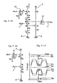
- a negative-feedback operational amplifier as shown in Fig. 1(b) of the accompanying drawings has been used as such a data inverting circuit.
- DC inverting reference voltage VREF is applied from an external source to a noninverting input terminal of operational amplifier 33, whose inverting input terminal is supplied with analog input signal VIN from input terminal 1 through resistor R31.
- Resistor R32 having the same resistance as that of resistor R31 is connected as a negative-feedback loop between the output terminal and the inverting input terminal of operational amplifier 33.
- the data inverting circuit produces an output signal VOUT from output terminal 2 connected to the output terminal of operational amplifier 33.
- the phase of output signal VOUT may change to a large extent due to the parasitic capacitance of feedback resistor R32. Since it is difficult to maintain a sufficient phase margin, the data inverting circuit may oscillate due to a positive feedback loop. Usually, the data inverting circuit is prevented from oscillating by inserting a phase-compensating capacitor (not shown). However, the phase-compensating capacitor delays the response of operational amplifier 33, which is thus unable to respond to quick input signals.
- a data inverting circuit for producing, from an analog input signal whose voltage is lower or higher than a constant DC voltage, an output signal having a waveform which is of inverted relationship to the waveform of the analog input signal with respect to the constant DC voltage as an axis of symmetry, comprising a voltage doubling circuit for generating a DC voltage which is twice the constant DC voltage as the axis of symmetry from a DC voltage supplied from an external source, and outputting the generated DC voltage between two terminals, and a bipolar transistor having a base connected to an input terminal to which the analog input signal is supplied, a collector connected to one of the two terminals through a series-connected circuit of a first resistor and a circuit for generating a voltage equal to the base-to-emitter forward voltage of the bipolar transistor, such that the bipolar transistor is forward-biased, and an emitter connected to the other of the two terminals through a second resistor having the same resistance as the first resistor, the arrangement being such that an output signal of the data inverting
- the data inverting circuit includes npn bipolar transistor Q1 having a base which is supplied with analog input signal VIN that is applied from an external source. Supplied analog input signal VIN is inverted and outputted to the collector of transistor Q1. The inverted voltage outputted to the collector of transistor Q1 is supplied through voltage follower 12 as output signal VOUT to output terminal 2 connected to the output terminal thereof.
- the data inverting circuit also has operational amplifier 13 for producing, from constant DC voltage (inverting reference voltage) VREF supplied from an external source, voltage 2VREF that is twice as high as inverting reference voltage VREF.
- Output voltage 2VREF from operational amplifier 13 is applied to the base of npn bipolar transistor Q2.
- Inverting reference voltage VREF is applied to a noninverting input terminal of operational amplifier 13 whose inverting input terminal is supplied with a voltage produced by resistors R10, R11 that divide the voltage from the output terminal of operational amplifier 13.
- Resistors R10, R11 have the same resistance for operational amplifier 13 to produce voltage 2VREF at its output terminal.
- Transistor Q2 produces at its emitter a voltage (2VREF - VF) which is equal to the difference between voltage 2VREF and base-to-emitter forward voltage VF of transistor Q2 (which is also equal to the base-to-emitter forward voltage of transistor Q1 as described below).
- the collector of transistor Q2 is connected to high-voltage power supply line 3.
- npn bipolar transistor Q3 The base of npn bipolar transistor Q3 is connected to the emitter of transistor Q1 in order to equalize currents flowing resistors R6 and R7.
- Transistor Q3 has an emitter connected to ground line 4 through resistor R9 and a collector to high-voltage power supply line 3 through resistor R8 which serves as a load.
- Transistors Q1, Q2, Q3, Q4, Q5 have the same characteristics, i.e., the same base-to-emitter forward voltage VF.
- Resistors R6, R7, R9 have the same resistance.
- collector current IC1 IE1 - IB1
- VN4 + VIN)/2 VREF.
- voltage VN4 at node N4 is practically equal to a voltage that is produced by inverting input signal voltage VIN with respect to inverting reference voltage VREF which serves as the axis of symmetry.
- Voltage VN4 is applied to voltage follower 12 for impedance conversion, and outputted as output signal VOUT from output terminal 2.
- the data inverting function of the data inverting circuit is achieved by a circuit composed of operational amplifier 13, two transistors Q2, Q1, and two resistors R6, R7. More specifically, as shown in Fig. 2(b), when input signal VIN is applied to the base of transistor Q1, it inverts input signal VIN and outputs the inverted signal to the collector thereof, i.e., to node N4. Since the resistance of resistor R6 connected to the collector of transistor Q1 and the resistance of resistor R7 connected to the emitter thereof are the same and the collector and emitter currents of transistor Q1 are substantially equal, the voltage drop across resistor R6 is equal to the voltage drop across resistor R7.
- voltage VN4 at node N4 which corresponds to output voltage VOUT, is lower than the voltage at node N2 by the voltage drop across resistor R6, and voltage VN5 at node N5 is higher than the ground potential by the voltage drop across resistor R7.
- the data inverting circuit according to the above embodiment basically has no resistor-feedback loop, it does not suffer oscillation induced by a positive-feedback loop and an operation delay.
- transistor Q3 Because of inserted transistor Q3, the collector current of transistor Q1, which flows through resistor R6, and the current flowing through resistor R7 are equal in magnitude at all times even when the magnitude of the base current of transistor Q1 varies, thus compensating for changes in the base current of transistor Q1. It is thus possible to increase the base current of transistor Q1 to increase the speed of inverting operation of the data inverting circuit.
- the data inverting circuit is therefore suitable for high-speed operation.
- transistor Q5 and resistor R7 in their series-connected circuit shown in Fig. 2(a) may be switched around in position.
- Transistor Q4 connected as a diode between resistor R6 and the collector of transistor Q1 serves to increase the voltage at node N2 by an increase, corresponding to base-to-emitter forward voltage VF, caused in the voltage at node N5 due to connection of transistor Q5, to thereby correct the voltage at node N4. Therefore, transistor Q4 and resistor R6 in their series-connected circuit shown may also be switched around in position.
- each of transistors Q2, Q4, Q5 shown in Fig. 2(a) may be replaced with a pn-junction diode.
- output signal voltage VOUT is represented by (2VREF - VIN) and does not depend on the base-to-emitter forward voltage of the transistor. Therefore, the data inverting circuit is more advantageous against temperature changes than the conventional data inverting circuit which employs a negative-feedback operational amplifier. Specifically, if voltage 2VREF is temperature-compensated, perature-compensated, then output voltage VOUT is in this embodiment. Since inverting reference voltage VREF is a constant DC voltage, it can be temperature-compensated with sufficient accuracy by employing temperature-compensating technology for reference voltages in large-scale semiconductor integrated circuits.
- the collector of transistor Q2 for generating voltage (2VREF - VF) from voltage 2VREF is connected to high-voltage power supply line 3.
- the base and collector of transistor Q2 may connected in common. Inasmuch as the voltage at node N2 is determined by the voltage at node N1, the voltage applied to the collector of transistor Q2 is not limited to the power supply voltage.
- input signal VIN whose voltage is lower than inverting reference voltage VREF is inverted into output signal VOUT whose voltage is higher than inverting reference voltage VREF.
- input signal VIN whose voltage is higher than inverting reference voltage VREF may be inverted into output signal VOUT whose voltage is lower than inverting reference voltage VREF.
- Fig. 3(a) shows the data inverting circuit according to the second embodiment of the present invention. Those parts shown in Fig. 3(a) which are identical to those shown in Fig. 2(a) are denoted by identical reference characters.
- analog input signal VIN that is applied from an external source to input terminal 1 is supplied to the base of pnp bipolar transistor Q21. Supplied analog input signal VIN is inverted and outputted to the collector of transistor Q21. The inverted voltage outputted to the collector of transistor Q21 is supplied through voltage follower 12 as output signal VOUT to output terminal 2 connected to the output terminal thereof.
- the data inverting circuit also has pnp bipolar transistor Q22 which is connected as a diode with the base and collector coupled in common to ground line 4.
- Transistor Q22 serves to produce a voltage that is higher than the ground voltage by base-to-emitter forward voltage VF of transistor Q21.
- a series-connected circuit of resistor R26 and pnp bipolar transistor Q24 which is connected as a diode with the base and collector coupled in common.
- a series-connected circuit of resistor R27 and pnp bipolar transistor Q25 which is connected as a diode with the base and collector coupled in common is connected to the emitter of transistor Q21.
- the emitter of transistor Q25 is connected to the output terminal of operational amplifier 13.
- Transistor Q23 for equalizing a collector current of transistor Q21 with a current flowing through resistor R27 is connected to the emitter of transistor Q21.
- Transistor Q23 has a collector connected to ground line 4 through resistor R28 which serves as a load and an emitter to the output terminal of operational amplifier 13 through resistor R28.
- Pnp bipolar transistors Q21, Q22, Q23, Q25, Q24 shown in Fig. 3(a) correspond respectively to transistor Q1 for inverting input signal VIN, transistor Q2 for generating the base-to-emitter forward voltage, transistor Q3 for compensating for changes in the base current, transistor Q5 for correcting the emitter voltage of transistor Q1, and transistor Q4 for correcting the collector voltage in the data inverting circuit according to the first embodiment.
- Resistors R26, R27, R28, R29 shown in Fig. 3(a) correspond respectively to resistors R6, R7, R8, R9 in the data inverting circuit according to the first embodiment.
- Transistors Q21, Q22, Q23, Q24, Q25 have the same characteristics, i.e., the same base-to-emitter forward voltage VF.
- Resistors R26, R27, R29 have the same resistance.
- the data inverting circuit according to the second embodiment is capable of symmetrically inverting input signal VIN whose voltage is higher than inverting reference voltage VREF into output signal VOUT whose voltage is lower than inverting reference voltage VREF.
- the operational amplifier is employed as a circuit for producing voltage 2VREF which is twice inverting reference voltage VREF, and inverting reference voltage VREF is applied to the noninverting input terminal of the operational amplifier for comparison with a voltage which is half the the voltage at its output terminal.
- the voltage applied to the noninverting input terminal of the operational amplifier is not limited to inverting reference voltage VREF.
- the operational amplifier can produce voltage 2VREF even when a voltage different from inverting reference voltage VREF is applied to the noninverting input terminal of the operational amplifier.
- the data inverting circuit according to each of the first and second embodiments may be implemented as a one-chip integrated circuit with equal transistor and resistor characteristics for increased accuracy of symmetry between the input and output signals.
- the transistors are disposed close together and the resistors are disposed close together on the chip, any variations in their characteristics depending on the fabrication process are minimized for increased operation accuracy.
- the chip is designed to orient the transistors and the resistors in one direction, any differences between their characteristics depending on the crystal direction (anisotropy) are reduced to make the data inverting circuit highly accurate.
- a voltage which is twice the inverting reference voltage applied from an external source is produced from the inverting reference voltage and outputted between two terminals.
- the collector of a data-inverting bipolar transistor whose base is supplied with an analog input signal is connected to one of the two terminals through a series-connected circuit of a resistor and a circuit for generating a voltage equal to the base-to-emitter forward voltage of the bipolar transistor, such that the bipolar transistor is forward-biased.
- the emitter of the bipolar transistor is connected to the other terminal through a resistor having the same resistance as the above resistor, with an output signal being produced from the collector of the bipolar transistor.
- the data inverting circuit can produce an output signal by inverting an analog input signal whose voltage is lower (or higher) than a constant DC voltage with respect to a hypothetical axis of symmetry which is represented by the constant DC voltage, without employing a resistor-feedback loop.
- the data inverting circuit is free of oscillation due to a negative-feedback loop, and operates at high speed without a delay in operation.
- the data inverting circuit includes a transistor for compensating for changes in the base current of the data-inverting bipolar transistor to keep the input and output signals symmetrical irrespective of the magnitude of the base current.
- the data inverting circuit can invert data with increased accuracy.
- the data inverting circuit also allows the base current of the data-inverting bipolar transistor to increase for operation at higher speed for data inversion.
- the data inverting circuit imposes no limitations on the input characteristics of a circuit connected next to the data inverting circuit.
Landscapes
- Physics & Mathematics (AREA)
- Nonlinear Science (AREA)
- Amplifiers (AREA)
- Liquid Crystal Display Device Control (AREA)
- Video Image Reproduction Devices For Color Tv Systems (AREA)
Claims (11)
- Dateninvertierungsschaltung, die aus einem analogen Eingangssignal (VIN), dessen Eingangsspannung sich zwischen zwei Pegeln verändert, die beide entweder niedriger oder höher als eine konstante Gleichspannung sind, ein Ausgangssignal (VOUT) erzeugt, dessen Signalform zur Signalform des analogen Eingangssignals in bezug auf die als Symmetrieachse dienende konstante Gleichspannung invertiert ist, mit:einer Spannungsverdopplungsschaltung (13, R10, R11), die aus einer von einer äußeren Quelle angelegten Invertierungsreferenzspannung eine Gleichspannung erzeugt, welche doppelt so groß wie die als die Symmetrieachse dienende konstante Gleichspannung ist, und die erzeugte Gleichspannung zwischen zwei Anschlüssen (N1, GND) ausgibt; undeinem Bipolartransistor (Q1), dessen Basis an einen Eingangsanschluß (1) angeschlossen ist, an den das analoge Eingangssignal angelegt wird, dessen Kollektor über eine Serienschaltung aus einem ersten Widerstand (R6) und aus einer Schaltung (Q2) zum Erzeugen einer Spannung, die gleich der Basis-Emitter-Vorwärtsspannung des Bipolartransistors ist, an einen der zwei Anschlüsse angeschlossen ist, derart, daß der Bipolartransistor in Vorwärtsrichtung vorgespannt ist, und dessen Emitter über einen zweiten Widerstand (R7), der den gleichen Widerstandswert wie der erste Widerstand (R6) besitzt, an den anderen der zwei Anschlüsse angeschlossen ist;wobei die Anordnung so beschaffen ist, daß vom Kollektor (N4) des Bipolartransistors (Q1) ein Ausgangssignal der Dateninvertierungsschaltung erzeugt wird.
- Dateninvertierungsschaltung nach Anspruch 1, in der der Bipolartransistor (Q1) ein npn-Ausgangsbipolartransistor ist und der andere der Anschlüsse ein Masseanschluß (GND) ist.
- Dateninvertierungsschaltung nach Anspruch 1 oder 2, in der die Spannungsverdopplungsschaltung (13, R10, R11) einen Operationsverstärker (13) enthält, der einen nichtinvertierenden Eingangsanschluß, an den die Invertierungsreferenzspannung (VREF) angelegt wird, und einen invertierenden Eingangsanschluß, an den eine Spannung angelegt wird, die halb so groß wie die Spannung an seinem Ausgangsanschluß ist, enthält, und die Spannungserzeugungsschaltung (Q2) einen npn-Bipolartransistor (Q2) enthält, an dessen Basis die von der Spannungsverdopplungsschaltung (13, R10, R11) erzeugte Spannung angelegt wird und dessen Emitter eine konstante Spannung ausgibt.
- Dateninvertierungsschaltung nach einem der Ansprüche 2 oder 3, ferner mit:einem npn-Bipolartransistor (Q3) zur Basistromkompensation, dessen Basis an den Emitter des Ausgangsbipolartransistors (Q1) angeschlossen ist und dessen Emitter über einen dritten Widerstand (R9), der den gleichen Widerstandswert wie der erste und der zweite Widerstandswert besitzt, an den Masseanschluß angeschlossen ist;einer npn-Diode (Q4) zur Kollektorspannungskorrektur, die mit dem ersten Widerstand (R6) in Serie geschaltet ist; undeiner npn-Diode (Q5) zur Emitterspannungskorrektur, die mit dem zweiten Widerstand (R7) in Serie geschaltet ist.
- Dateninvertierungsschaltung, die aus einem analogen Eingangssignal (VIN), dessen Spannung sich zwischen zwei Pegeln verändert, die beide höher als eine konstante Gleichspannung (VREF) sind, ein Ausgangssignal (vOUT) erzeugt, dessen Signalform zur Signalform des analogen Eingangssignals in bezug auf die als Symmetrieachse dienende konstante Gleichspannung (VREF) invertiert ist, mit:einem pnp-Ausgangsbipolartransistor (Q21), an dessen Basis das analoge Eingangssignal angelegt wird;einer Spannungsverdopplungsschaltung (13, R10, R11), die aus einer von einer äußeren Quelle angelegten Invertierungsreferenzspannung eine Gleichspannung erzeugt, die doppelt so groß wie die als die Symmetrieachse dienende konstante Gleichspannung ist;einer Konstantspannungserzeugungsschaltung (Q22) zum Erzeugen einer konstanten Spannung, die um eine Spannung, die gleich der Basis-Emitter-Spannung des Ausgangsbipolartransistors (Q21) ist, höher als eine Massespannung ist;einem ersten Widerstand (R26), der zwischen einen Ausgangsanschluß der Konstantspannungserzeugungsschaltung (Q22) und den Kollektor des Ausgangsbipolartransistors (Q21) geschaltet ist; undeinem zweiten Widerstand (R27), der zwischen einen Ausgangsanschluß der Spannungsverdopplungsschaltung und den Emitter des Ausgangsbipolartransistors geschaltet ist, wobei der zweite Widerstand (R27) den gleichen Widerstandswert wie der erste Widerstand (R26) besitzt;wobei die Anordnung so beschaffen ist, daß aus dem Kollektor (N24) des Ausgangsbipolartransistors ein Ausgangssignal der Dateninvertierungsschaltung erzeugt wird.
- Dateninvertierungsschaltung nach Anspruch 5, in der die Spannungsverdopplungsschaltung (13) einen Operationsverstärker (13, R10, R11) enthält, der einen nichtinvertierenden Eingangsanschluß, an den die Invertierungsreferenzspannung angelegt wird, und einen invertierenden Eingangsanschluß, an den eine Spannung angelegt wird, die halb so groß wie die Spannung an seinem Ausgangsanschluß ist, enthält, und die Konstantspannungserzeugungsschaltung (Q22) einen pnp-Bipolartransistor (Q22) enthält, die als Diode geschaltet ist, indem seine Basis und sein Kollektor miteinander verbunden sind, und dessen Emitter (N26) die Konstantspannung ausgibt.
- Dateninvertierungsschaltung nach den Ansprüchen 5 oder 6, ferner mit:einem pnp-Bipolartransistor (Q23) zur Basisstromkompensation, dessen Basis an den Emitter des Ausgangsbipolartransistors (Q21) angeschlossen ist und dessen Emitter über einen dritten Widerstand (R29), der den gleichen Widerstandswert wie der erste und der zweite Widerstand besitzt, an den Ausgangsanschluß der Spannungsverdopplungsschaltung (13, R10, R11) angeschlossen ist;einer pnp-Diode (Q24) zur Kollektorspannungskorrektur, die mit dem ersten Widerstand (R26) in Serie geschaltet ist; undeiner pnp-Diode (Q25) zur Emitterspannungskorrektur, die mit dem zweiten Widerstand (R27) in Serie geschaltet ist.
- Dateninvertierungsschaltung nach einem der Ansprüche 1 bis 4, ferner mit einem Spannungsfolger (12), der das Ausgangssignal vom Kollektor des Ausgangsbipolartransistors (Q1) überträgt.
- Dateninvertierungsschaltung nach einem der Ansprüche 5 bis 7, ferner mit einem Spannungsfolger (12), der das Ausgangssignal vom Emitter des Ausgangsbipolartransistors (Q21) überträgt.
- Dateninvertierungsschaltung nach einem der Ansprüche 1 bis 4, in der der Ausgangsbipolartransistor (Q1), der Bipolartransistor der Konstantspannungserzeugungsschaltung (Q2), der pnp-Bipolartransistor (Q3) zur Basisstromkorrektur, der pnp-Bipolartransistor (Q5) zur Emitterspannungskorrektur und der pnp-Bipolartransistor (Q4) zur Kollektorspannungskorrektur sowie der erste Widerstand (R6), der zweite Widerstand (R7) und der dritte Widerstand (R9) die gleichen Transistor- bzw. Widerstandskennlinien besitzen und auf einem Halbleitersubstrat nahe beieinander und in der gleichen Richtung orientiert angeordnet sind.
- Dateninvertierungsschaltung nach einem der Ansprüche 5 bis 7, in dem der Ausgangsbipolartransistor (Q21), der Bipolartransistor der Konstantspannungserzeugungsschaltung (Q22), der pnp-Bipolartransistor (Q23) zur Basisstromkorrektur, der pnp-Bipolartransistor (Q25) zur Ermitterspannungskorrektur und der pnp-Bipolartransistor (Q24) zur Kollektorspannungskorrektur sowie der erste Widerstand (R26), der zweite Widerstand (R27) und der dritte Widerstand (R29) die gleichen Transistor- bzw. Widerstandskennlinien besitzen und auf einem Halbleitersubstrat nahe beieinander und in der gleichen Richtung orientiert angeordnet sind.
Applications Claiming Priority (2)
| Application Number | Priority Date | Filing Date | Title |
|---|---|---|---|
| JP5000167A JP2581388B2 (ja) | 1993-01-05 | 1993-01-05 | データ反転回路 |
| JP167/93 | 1993-01-05 |
Publications (3)
| Publication Number | Publication Date |
|---|---|
| EP0606060A2 EP0606060A2 (de) | 1994-07-13 |
| EP0606060A3 EP0606060A3 (de) | 1995-01-18 |
| EP0606060B1 true EP0606060B1 (de) | 1998-04-01 |
Family
ID=11466477
Family Applications (1)
| Application Number | Title | Priority Date | Filing Date |
|---|---|---|---|
| EP94100024A Expired - Lifetime EP0606060B1 (de) | 1993-01-05 | 1994-01-03 | Bipolare invertierende Pegelumsetzer mit Einheitsverstärkung |
Country Status (5)
| Country | Link |
|---|---|
| US (1) | US5416433A (de) |
| EP (1) | EP0606060B1 (de) |
| JP (1) | JP2581388B2 (de) |
| KR (1) | KR970007752B1 (de) |
| DE (1) | DE69409263T2 (de) |
Family Cites Families (7)
| Publication number | Priority date | Publication date | Assignee | Title |
|---|---|---|---|---|
| US4527078A (en) * | 1982-08-23 | 1985-07-02 | Signetics Corporation | Signal translator with supply voltage compensation particularly for use as interface between current tree logic and transistor-transistor logic |
| US4578602A (en) * | 1983-07-11 | 1986-03-25 | Signetics Corporation | Voltage signal translator |
| JPS6294005A (ja) * | 1985-10-21 | 1987-04-30 | Toshiba Corp | 広帯域増幅回路 |
| JPH01206708A (ja) * | 1988-02-12 | 1989-08-18 | Sumitomo Electric Ind Ltd | 増幅回路 |
| JPH02253231A (ja) * | 1989-03-28 | 1990-10-12 | Toshiba Corp | 液晶表示装置及びその調整方法 |
| JPH03198089A (ja) * | 1989-12-27 | 1991-08-29 | Sharp Corp | 液晶表示装置の駆動回路 |
| JPH047907A (ja) * | 1990-04-25 | 1992-01-13 | Matsushita Electric Ind Co Ltd | Dcシフト回路 |
-
1993
- 1993-01-05 JP JP5000167A patent/JP2581388B2/ja not_active Expired - Fee Related
-
1994
- 1994-01-03 DE DE69409263T patent/DE69409263T2/de not_active Expired - Lifetime
- 1994-01-03 EP EP94100024A patent/EP0606060B1/de not_active Expired - Lifetime
- 1994-01-04 KR KR94000064A patent/KR970007752B1/ko not_active Expired - Lifetime
- 1994-01-04 US US08/177,756 patent/US5416433A/en not_active Expired - Lifetime
Also Published As
| Publication number | Publication date |
|---|---|
| DE69409263D1 (de) | 1998-05-07 |
| JP2581388B2 (ja) | 1997-02-12 |
| US5416433A (en) | 1995-05-16 |
| KR970007752B1 (en) | 1997-05-16 |
| JPH06204760A (ja) | 1994-07-22 |
| EP0606060A3 (de) | 1995-01-18 |
| DE69409263T2 (de) | 1998-12-17 |
| EP0606060A2 (de) | 1994-07-13 |
Similar Documents
| Publication | Publication Date | Title |
|---|---|---|
| US4525682A (en) | Biased current mirror having minimum switching delay | |
| JP2526278B2 (ja) | 電圧制御発振器 | |
| US5721505A (en) | Delay circuit manufacturable by semiconductor elements | |
| JP2000244251A (ja) | 補償回路 | |
| JP2542722B2 (ja) | 非対称信号生成回路 | |
| US5262690A (en) | Variable delay clock circuit | |
| EP0606060B1 (de) | Bipolare invertierende Pegelumsetzer mit Einheitsverstärkung | |
| JPS59185419A (ja) | 周波数―位相変換器 | |
| US4974916A (en) | Integratable circuit arrangement for delaying pulse-shaped signals | |
| US5155429A (en) | Threshold voltage generating circuit | |
| JP2896029B2 (ja) | 電圧電流変換回路 | |
| JPS6331214A (ja) | 可変遅延回路 | |
| US6466097B1 (en) | Phase locked loop and associated control method | |
| JPS6252486B2 (de) | ||
| EP0484921B1 (de) | Differentialschaltung zur Umsetzung eines Einphasen-Signals in ein Komplementärsignal | |
| US4596960A (en) | Current mirror circuit | |
| JP2500424B2 (ja) | 入力整数倍反転回路 | |
| JPH09148894A (ja) | 電源電圧の変動に強い電圧制御発振器 | |
| SU1626327A1 (ru) | Дифференциальный усилитель | |
| JPS61294919A (ja) | 電圧制御発振回路 | |
| JP2755219B2 (ja) | 発振回路 | |
| SU1686694A1 (ru) | Транзисторный фазоинвертор | |
| JPS6192005A (ja) | 発振回路 | |
| JPS60158764A (ja) | 電話機用電源回路 | |
| JPS61202514A (ja) | のこぎり波発生回路 |
Legal Events
| Date | Code | Title | Description |
|---|---|---|---|
| PUAI | Public reference made under article 153(3) epc to a published international application that has entered the european phase |
Free format text: ORIGINAL CODE: 0009012 |
|
| AK | Designated contracting states |
Kind code of ref document: A2 Designated state(s): DE FR GB |
|
| PUAL | Search report despatched |
Free format text: ORIGINAL CODE: 0009013 |
|
| AK | Designated contracting states |
Kind code of ref document: A3 Designated state(s): DE FR GB |
|
| 17P | Request for examination filed |
Effective date: 19950505 |
|
| 17Q | First examination report despatched |
Effective date: 19961002 |
|
| GRAG | Despatch of communication of intention to grant |
Free format text: ORIGINAL CODE: EPIDOS AGRA |
|
| GRAG | Despatch of communication of intention to grant |
Free format text: ORIGINAL CODE: EPIDOS AGRA |
|
| GRAH | Despatch of communication of intention to grant a patent |
Free format text: ORIGINAL CODE: EPIDOS IGRA |
|
| GRAH | Despatch of communication of intention to grant a patent |
Free format text: ORIGINAL CODE: EPIDOS IGRA |
|
| GRAA | (expected) grant |
Free format text: ORIGINAL CODE: 0009210 |
|
| AK | Designated contracting states |
Kind code of ref document: B1 Designated state(s): DE FR GB |
|
| REF | Corresponds to: |
Ref document number: 69409263 Country of ref document: DE Date of ref document: 19980507 |
|
| ET | Fr: translation filed | ||
| PLBE | No opposition filed within time limit |
Free format text: ORIGINAL CODE: 0009261 |
|
| STAA | Information on the status of an ep patent application or granted ep patent |
Free format text: STATUS: NO OPPOSITION FILED WITHIN TIME LIMIT |
|
| 26N | No opposition filed | ||
| REG | Reference to a national code |
Ref country code: GB Ref legal event code: IF02 |
|
| REG | Reference to a national code |
Ref country code: GB Ref legal event code: 732E |
|
| REG | Reference to a national code |
Ref country code: FR Ref legal event code: TP |
|
| REG | Reference to a national code |
Ref country code: GB Ref legal event code: 732E Free format text: REGISTERED BETWEEN 20100325 AND 20100331 |
|
| REG | Reference to a national code |
Ref country code: GB Ref legal event code: 732E Free format text: REGISTERED BETWEEN 20101111 AND 20101117 |
|
| REG | Reference to a national code |
Ref country code: FR Ref legal event code: TP |
|
| REG | Reference to a national code |
Ref country code: DE Ref legal event code: R081 Ref document number: 69409263 Country of ref document: DE Owner name: CHIMEI INNOLUX CORP., TW Free format text: FORMER OWNER: NEC CORP., TOKYO, JP Effective date: 20110331 |
|
| PGFP | Annual fee paid to national office [announced via postgrant information from national office to epo] |
Ref country code: FR Payment date: 20120130 Year of fee payment: 19 |
|
| PGFP | Annual fee paid to national office [announced via postgrant information from national office to epo] |
Ref country code: DE Payment date: 20120127 Year of fee payment: 19 |
|
| PGFP | Annual fee paid to national office [announced via postgrant information from national office to epo] |
Ref country code: GB Payment date: 20120126 Year of fee payment: 19 |
|
| GBPC | Gb: european patent ceased through non-payment of renewal fee |
Effective date: 20130103 |
|
| REG | Reference to a national code |
Ref country code: FR Ref legal event code: ST Effective date: 20130930 |
|
| PG25 | Lapsed in a contracting state [announced via postgrant information from national office to epo] |
Ref country code: DE Free format text: LAPSE BECAUSE OF NON-PAYMENT OF DUE FEES Effective date: 20130801 |
|
| PG25 | Lapsed in a contracting state [announced via postgrant information from national office to epo] |
Ref country code: GB Free format text: LAPSE BECAUSE OF NON-PAYMENT OF DUE FEES Effective date: 20130103 Ref country code: FR Free format text: LAPSE BECAUSE OF NON-PAYMENT OF DUE FEES Effective date: 20130131 |
|
| REG | Reference to a national code |
Ref country code: DE Ref legal event code: R119 Ref document number: 69409263 Country of ref document: DE Effective date: 20130801 |