EP0608503B1 - Dispositif semi-conducteur et son procédé de fabrication - Google Patents
Dispositif semi-conducteur et son procédé de fabrication Download PDFInfo
- Publication number
- EP0608503B1 EP0608503B1 EP93118615A EP93118615A EP0608503B1 EP 0608503 B1 EP0608503 B1 EP 0608503B1 EP 93118615 A EP93118615 A EP 93118615A EP 93118615 A EP93118615 A EP 93118615A EP 0608503 B1 EP0608503 B1 EP 0608503B1
- Authority
- EP
- European Patent Office
- Prior art keywords
- temperature
- film
- polycrystalline silicon
- solid phase
- amorphous
- Prior art date
- Legal status (The legal status is an assumption and is not a legal conclusion. Google has not performed a legal analysis and makes no representation as to the accuracy of the status listed.)
- Expired - Lifetime
Links
Images




Classifications
-
- H—ELECTRICITY
- H10—SEMICONDUCTOR DEVICES; ELECTRIC SOLID-STATE DEVICES NOT OTHERWISE PROVIDED FOR
- H10P—GENERIC PROCESSES OR APPARATUS FOR THE MANUFACTURE OR TREATMENT OF DEVICES COVERED BY CLASS H10
- H10P14/00—Formation of materials, e.g. in the shape of layers or pillars
- H10P14/20—Formation of materials, e.g. in the shape of layers or pillars of semiconductor materials
- H10P14/24—Formation of materials, e.g. in the shape of layers or pillars of semiconductor materials using chemical vapour deposition [CVD]
-
- H—ELECTRICITY
- H10—SEMICONDUCTOR DEVICES; ELECTRIC SOLID-STATE DEVICES NOT OTHERWISE PROVIDED FOR
- H10D—INORGANIC ELECTRIC SEMICONDUCTOR DEVICES
- H10D30/00—Field-effect transistors [FET]
- H10D30/01—Manufacture or treatment
- H10D30/021—Manufacture or treatment of FETs having insulated gates [IGFET]
- H10D30/031—Manufacture or treatment of FETs having insulated gates [IGFET] of thin-film transistors [TFT]
- H10D30/0312—Manufacture or treatment of FETs having insulated gates [IGFET] of thin-film transistors [TFT] characterised by the gate electrodes
- H10D30/0314—Manufacture or treatment of FETs having insulated gates [IGFET] of thin-film transistors [TFT] characterised by the gate electrodes of lateral top-gate TFTs comprising only a single gate
-
- H—ELECTRICITY
- H10—SEMICONDUCTOR DEVICES; ELECTRIC SOLID-STATE DEVICES NOT OTHERWISE PROVIDED FOR
- H10D—INORGANIC ELECTRIC SEMICONDUCTOR DEVICES
- H10D30/00—Field-effect transistors [FET]
- H10D30/01—Manufacture or treatment
- H10D30/021—Manufacture or treatment of FETs having insulated gates [IGFET]
- H10D30/031—Manufacture or treatment of FETs having insulated gates [IGFET] of thin-film transistors [TFT]
- H10D30/0321—Manufacture or treatment of FETs having insulated gates [IGFET] of thin-film transistors [TFT] comprising silicon, e.g. amorphous silicon or polysilicon
-
- H—ELECTRICITY
- H10—SEMICONDUCTOR DEVICES; ELECTRIC SOLID-STATE DEVICES NOT OTHERWISE PROVIDED FOR
- H10D—INORGANIC ELECTRIC SEMICONDUCTOR DEVICES
- H10D30/00—Field-effect transistors [FET]
- H10D30/60—Insulated-gate field-effect transistors [IGFET]
- H10D30/67—Thin-film transistors [TFT]
- H10D30/6729—Thin-film transistors [TFT] characterised by the electrodes
- H10D30/673—Thin-film transistors [TFT] characterised by the electrodes characterised by the shapes, relative sizes or dispositions of the gate electrodes
- H10D30/6731—Top-gate only TFTs
-
- H—ELECTRICITY
- H10—SEMICONDUCTOR DEVICES; ELECTRIC SOLID-STATE DEVICES NOT OTHERWISE PROVIDED FOR
- H10D—INORGANIC ELECTRIC SEMICONDUCTOR DEVICES
- H10D30/00—Field-effect transistors [FET]
- H10D30/60—Insulated-gate field-effect transistors [IGFET]
- H10D30/67—Thin-film transistors [TFT]
- H10D30/6729—Thin-film transistors [TFT] characterised by the electrodes
- H10D30/6737—Thin-film transistors [TFT] characterised by the electrodes characterised by the electrode materials
- H10D30/6739—Conductor-insulator-semiconductor electrodes
-
- H—ELECTRICITY
- H10—SEMICONDUCTOR DEVICES; ELECTRIC SOLID-STATE DEVICES NOT OTHERWISE PROVIDED FOR
- H10D—INORGANIC ELECTRIC SEMICONDUCTOR DEVICES
- H10D30/00—Field-effect transistors [FET]
- H10D30/60—Insulated-gate field-effect transistors [IGFET]
- H10D30/67—Thin-film transistors [TFT]
- H10D30/674—Thin-film transistors [TFT] characterised by the active materials
- H10D30/6741—Group IV materials, e.g. germanium or silicon carbide
- H10D30/6743—Silicon
- H10D30/6745—Polycrystalline or microcrystalline silicon
-
- H—ELECTRICITY
- H10—SEMICONDUCTOR DEVICES; ELECTRIC SOLID-STATE DEVICES NOT OTHERWISE PROVIDED FOR
- H10P—GENERIC PROCESSES OR APPARATUS FOR THE MANUFACTURE OR TREATMENT OF DEVICES COVERED BY CLASS H10
- H10P14/00—Formation of materials, e.g. in the shape of layers or pillars
- H10P14/20—Formation of materials, e.g. in the shape of layers or pillars of semiconductor materials
- H10P14/29—Formation of materials, e.g. in the shape of layers or pillars of semiconductor materials characterised by the substrates
- H10P14/2901—Materials
- H10P14/2921—Materials being crystalline insulating materials
-
- H—ELECTRICITY
- H10—SEMICONDUCTOR DEVICES; ELECTRIC SOLID-STATE DEVICES NOT OTHERWISE PROVIDED FOR
- H10P—GENERIC PROCESSES OR APPARATUS FOR THE MANUFACTURE OR TREATMENT OF DEVICES COVERED BY CLASS H10
- H10P14/00—Formation of materials, e.g. in the shape of layers or pillars
- H10P14/20—Formation of materials, e.g. in the shape of layers or pillars of semiconductor materials
- H10P14/29—Formation of materials, e.g. in the shape of layers or pillars of semiconductor materials characterised by the substrates
- H10P14/2901—Materials
- H10P14/2922—Materials being non-crystalline insulating materials, e.g. glass or polymers
-
- H—ELECTRICITY
- H10—SEMICONDUCTOR DEVICES; ELECTRIC SOLID-STATE DEVICES NOT OTHERWISE PROVIDED FOR
- H10P—GENERIC PROCESSES OR APPARATUS FOR THE MANUFACTURE OR TREATMENT OF DEVICES COVERED BY CLASS H10
- H10P14/00—Formation of materials, e.g. in the shape of layers or pillars
- H10P14/20—Formation of materials, e.g. in the shape of layers or pillars of semiconductor materials
- H10P14/32—Formation of materials, e.g. in the shape of layers or pillars of semiconductor materials characterised by intermediate layers between substrates and deposited layers
- H10P14/3202—Materials thereof
- H10P14/3204—Materials thereof being Group IVA semiconducting materials
- H10P14/3211—Silicon, silicon germanium or germanium
-
- H—ELECTRICITY
- H10—SEMICONDUCTOR DEVICES; ELECTRIC SOLID-STATE DEVICES NOT OTHERWISE PROVIDED FOR
- H10P—GENERIC PROCESSES OR APPARATUS FOR THE MANUFACTURE OR TREATMENT OF DEVICES COVERED BY CLASS H10
- H10P14/00—Formation of materials, e.g. in the shape of layers or pillars
- H10P14/20—Formation of materials, e.g. in the shape of layers or pillars of semiconductor materials
- H10P14/32—Formation of materials, e.g. in the shape of layers or pillars of semiconductor materials characterised by intermediate layers between substrates and deposited layers
- H10P14/3258—Crystal orientation
-
- H—ELECTRICITY
- H10—SEMICONDUCTOR DEVICES; ELECTRIC SOLID-STATE DEVICES NOT OTHERWISE PROVIDED FOR
- H10P—GENERIC PROCESSES OR APPARATUS FOR THE MANUFACTURE OR TREATMENT OF DEVICES COVERED BY CLASS H10
- H10P14/00—Formation of materials, e.g. in the shape of layers or pillars
- H10P14/20—Formation of materials, e.g. in the shape of layers or pillars of semiconductor materials
- H10P14/34—Deposited materials, e.g. layers
- H10P14/3402—Deposited materials, e.g. layers characterised by the chemical composition
- H10P14/3404—Deposited materials, e.g. layers characterised by the chemical composition being Group IVA materials
- H10P14/3411—Silicon, silicon germanium or germanium
-
- H—ELECTRICITY
- H10—SEMICONDUCTOR DEVICES; ELECTRIC SOLID-STATE DEVICES NOT OTHERWISE PROVIDED FOR
- H10P—GENERIC PROCESSES OR APPARATUS FOR THE MANUFACTURE OR TREATMENT OF DEVICES COVERED BY CLASS H10
- H10P14/00—Formation of materials, e.g. in the shape of layers or pillars
- H10P14/20—Formation of materials, e.g. in the shape of layers or pillars of semiconductor materials
- H10P14/34—Deposited materials, e.g. layers
- H10P14/3451—Structure
- H10P14/3452—Microstructure
- H10P14/3456—Polycrystalline
-
- H—ELECTRICITY
- H10—SEMICONDUCTOR DEVICES; ELECTRIC SOLID-STATE DEVICES NOT OTHERWISE PROVIDED FOR
- H10P—GENERIC PROCESSES OR APPARATUS FOR THE MANUFACTURE OR TREATMENT OF DEVICES COVERED BY CLASS H10
- H10P14/00—Formation of materials, e.g. in the shape of layers or pillars
- H10P14/20—Formation of materials, e.g. in the shape of layers or pillars of semiconductor materials
- H10P14/38—Formation of materials, e.g. in the shape of layers or pillars of semiconductor materials characterised by treatments done after the formation of the materials
- H10P14/3802—Crystallisation or recrystallisation of non-monocrystalline semiconductor materials, e.g. regrowth
Definitions
- This invention relates to a semiconductor device comprising CMOS type field effect transistors and to its manufacturing method, in particular, a semiconductor device on an insulating material and its manufacturing method.
- insulating materials such as insulating amorphous substrates, for example, glass, quartz or the like, insulating amorphous layers, for example SiO 2 , Si 3 N 4 and the like, and so forth.
- TFT thin film transistor
- the following methods have been studied: (1) TFT comprising amorphous silicon formed by plasma CVD or the like as an element material, (2) TFT comprising polycrystalline silicon formed by CVD or the like as an element material, (3) TFT comprising single crystalline silicon formed by fusion recrystallization or the like as an element material, and the like.
- TFTs comprising amorphous silicon or polycrystalline silicon are substantially lower than that of TFTs comprising single crystalline silicon (amorphous silicon TFTs ⁇ 1 cm 2 /V.sec, polycrystalline silicon TFT about 10cm 2 N/V.sec).
- the conventional method of the prior art is that, first polycrystalline silicon is formed by CVD, and after said polycrystalline silicon is amorphized by Si + ion implantation, heat treatment is performed at approximately 600°C for nearly 100 hours. Because of that, there are such problems as: (1) since polycrystalline silicon is amorphized after if has once been formed, the process is complicated causing a cost up, (2) an expensive ion implantation system is necessary, (3) the heat treatment is extremely long, (4) it is very hard to handle a large substrate (for example, 30 cm x 30 cm), (5) the crystallized volume fraction after solid phase recrystallization is low and, therefore, it is very difficult to fabricate a high quality semiconductor device, and the like.
- a semiconductor device comprising CMOS type field effect transistors whose gate electrodes of both the P-channel and N-channel transistors are of n + type polycrystalline silicon is disclosed in EP-A-0 296 747.
- the document US-A-4,448,632 discloses a method of forming a monocrystalline silicon layer by first forming a polycrystalline silicon layer on an amorphous substrate, increasing the grain size of the polycrystalline layer to 5 ⁇ m and more by laser fusion recrystallization, forming an epitaxial layer on the polycrystalline layer and converting the two layers into monocrystalline silicon by a second step of laser fusion recrystallization.
- US-A-4,249,957 discloses p and n type polycrystalline silicon for use in a solar cell, which has a grain size of 0.05 to 0.5 mm.
- US-A-4,129,463 discloses a method of forming uniformly n type phosphorousdoped polycrystalline silicon having a mean grain size of less than 1000 ⁇ m suitable for use in photovoltaic devices.
- It is an object of this invention is to provide means to realize a high quality semiconductor device including CMOS type field effect transistors wherein good TFT characteristics can be obtained in both p channel and n channel without requiring channel doping.
- This object is achieved with a semiconductor device and a manufacturing method as claimed.
- Fig. 1 shows one example of the manufacturing process of a semiconductor device. The case wherein a thin film transistor (TFT) is formed as a semiconductor element is shown as an example in Fig. 1.
- TFT thin film transistor
- Fig. 1(a) shows a process of forming a silicon layer 102 over an insulating material 101, such as an insulating amorphous substrate, for example, glass, quartz and the like, an insulating amorphous material layer, for example, SiO 2 , Si 3 N 4 and the like, and so forth.
- insulating material 101 such as an insulating amorphous substrate, for example, glass, quartz and the like, an insulating amorphous material layer, for example, SiO 2 , Si 3 N 4 and the like, and so forth.
- Other insulating crystalline substrates such as a sapphire substrate (Al 2 O 3 ), MgO.Al 2 O 3 , BP, CaF 2 , and the like can also be employed as a substrate instead of quartz and glass.
- a silicon layer is formed at a thickness of about 0.01 - 0.2 ⁇ m on a desired substrate by plasma CVD.
- the method of forming the film is not limited to the foregoing.
- Fig. 1(b) shows a process of forming a polycrystalline silicon layer 103 via crystal growth by performing a thermal treatment or the like on said silicon layer 102.
- the best condition of the thermal treatment differs depending upon the method of forming the silicon layer in process (a). For example, depending upon the substrate temperature difference at the time of forming the silicon layer, there are differences as follows:
- a thermal treatment condition is described hereinafter. After an amorphous silicon film has been formed by plasma CVD, the film is annealed before vacuum is broken. Since an amorphous film formed at low temperature becomes porous, if it is taken out to the air as is after the film growth, then oxygen and the like will enter into the film rendering a low quality film.
- the film is given proper thermal treatment before it is taken out to the air, then the film becomes dense, thereby preventing oxygen from entering in the film.
- the desirable thermal treatment temperature is over 300°C, and if the temperature is raised to approximately 400 to 500°C, substantially effective results can be achieved. Also, even when the thermal treatment temperature is lower than 300°C, film densification can be achieved. However, when annealing for solid phase recrystallization is continuously performed without breaking vacuum, the above annealing can be omitted.
- said amorphous silicon film undergoes a thermal treatment or the like for solid phase recrystallization.
- thermal treatment of about 550°C to 650°C is performed for about several hours to 20 hours on an amorphous silicon film which was formed at low temperature, hydrogen removal and crystal growth occur, and polycrystalline silicon containing large grains of about ⁇ (1 to 2 ⁇ m) is formed.
- the amount of hydrogen in a film is less if the film is formed when the substrate temperature is in the range of 150°C to 300°C compared to an amorphous silicon film formed at low temperature as described above; however, the temperature shifts to a higher degree when hydrogen removal starts. Since the film is more dense compared to the film formed at lower temperature, the annealing for achieving density can be omitted.
- solid phase recrystallization is performed under the thermal treatment temperature of 550°C to 650°C for about several hours to 40 hours, then hydrogen removal and crystal growth occur, and polycrystalline silicon containing large grains of about 1 to 2 ⁇ m is formed.
- the substrate temperature of 150°C to 200°C is particularly desirable because large grains can be formed and film separation, which may occur during temperature rise to the prescribed degree for solid phase recrystallization does not occur easily.
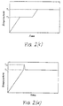
- Fig. 2 shows graphic illustrations of examples of the method of raising the temperature.
- Fig. 2(a) shows the case wherein, first, the temperature is raised to the prescribed level (T 1 ) at the specified temperature rise speed and then annealing is performed at this prescribed level (T 1 ).
- T 1 the prescribed level
- T 2(a) the desirable temperature rise speed is less than 20°C/min (preferably it is 5°C/min) so that occurrence of defects associated with hydrogen removal is suppressed.
- the temperature rise speed need not be constantly the same, but it can fluctuate within the foregoing range.
- T 2(b) shows the case wherein, first, the temperature is raised to the prescribed level (T 2 ) at the specified temperature rise speed, then the temperature is further raised to the annealing temperature of T 1 by a lower temperature rise speed.
- the reason for the change of the temperature rise speed around T 2 is that, as it was mentioned previously, hydrogen removal in the film starts at a temperature higher than about 300°C. Therefore, after hydrogen removal has started, the temperature rise speed is slowed down to less than 20°C/min (preferably 5°C/min) so as to suppress the occurrence of defects (it also contributes to shorten the temperature rise time.)
- the desirable level of T 2 is about 250°C to 400°C. Also, as in the case of Fig. 2(a), the temperature rise speed need not be constantly the same.
- Fig. 2(c) shows the case wherein, first, the temperature is raised to T 2 , then T 2 is maintained for a certain time and then the temperature is further raised to the annealing temperature of T 1 .
- a large amount of hydrogen in the film can be removed without generating polycrystalline nuclei by maintaining a temperature lower than the annealing temperature for a certain time (for example, about 20 minutes to 2 hours).
- T 2 is about 350°C to 550°C.
- T 2 need not be constantly the same. For example, it is alright to slowly raise the temperature by less than 5°C/min.
- T 2(d) shows the case wherein, first, the temperature is raised to the annealing temperature of T 1 , then the temperature is raised in a period of several minutes to T 3 , which is higher than the annealing temperature, then the temperature is cooled down to T 1 in a period of several minutes and then annealing is performed at T 1 .
- T 3 By having the step of raising the temperature to T 3 , crystalline growth can be progressed with complete hydrogen removal, compared to the time when crystalline growth is hindered by hydrogen in the film at the time of annealing at about 550°C to 650°C.
- the desirable value of T 3 is about 700°C to 800°C.
- amorphous silicon films can be produced in quantities by plasma CVD and they can be applied in a large area, since the hydrogen content in the film is large and the hydrogen hinders solid phase recrystallization, it was thought that thus was not a desirable method for forming an amorphous silicon film on which solid phase recrystallization is to be performed.
- Fig. 1(c) shows a process of forming a gate insulation film 104 by oxidizing said polycrystalline silicon layer 103 by thermal oxidation.
- the gate oxidation temperature is approximately 1,000°C to 1,200°C.
- Polycrystalline silicon layer 103 was formed by solid phase recrystallization described in the process (b), however, the crystallized volume fraction is not necessarily high.
- a silicon film formed by plasma CVD amorphous silicon or micro-crystalline silicon, which has minute crystal regions in the amorphous phase were generated
- the crystallized volume fraction is low at approximately 40% to 85% (it varies depending upon the film growth condition and solid phase recrystallization).
- the substrate temperature of a film formed by plasma CVD and the method of temperature rise at the time of gate oxidation have a profound relationship. That is, (1) the higher the substrate temperature is, the smaller the amount of hydrogen content in the film. When the substrate temperature is over 350°C, preferably over 400°C, hydrogen content in the film decreases extremely. Thus, the occurrence of defects associated with hydrogen removal during the temperature rise to the solid phase recrystallization temperature of 550°C to 650°C decreases.
- An amorphous silicon film formed by plasma CVD contains less contaminants, e.g. oxygen (O), nitrogen (N), or carbon (C), compared to the amorphous silicon film formed by electron beam evaporation or LPCVD.
- O oxygen
- N nitrogen
- C carbon
- the amorphous silicon deposited at a temperature range of about 150°C to 350°C contains the lowest amount of contaminants which is derived from an insulating support, and a reactor chamber of PCVD.
- the amorphous silicon deposited at a temperature range of about room temperature to 150°C releases hydrogen easily by heat treatment, which makes heat treatment time short.
- the amount of C and O in an amorphous silicon formed by PCVD can be reduced to the order of 10E17 to 10E18 cmE-3. Particularly, it is also possible to reduce the amount of C and O to less than 10E16 by improving purity of gas source, and suppressing generation of contaminants for inner wall if the reactor chamber.
- a very important relationship between the film growth temperature of a film formed by LPCVD and the method of temperature rise at the time of gate oxidation is described hereinafter.
- a silicon layer formed at high temperature for example, about 580°C to 610°C
- a silicon layer formed at low temperature for example, about 500°C to 550°C
- TFT field effect mobility is smaller.
- a silicon layer formed at low temperature formed larger grains and achieved higher crystallized volume fraction and higher field effect mobility.
- the method explained above is effective in the following cases besides for a film formed by LPCVD and CVD: (1) in the case wherein amorphous silicon or micro-crystalline silicon is formed by vapor deposition, EB vapor deposition, MBE, sputtering, ECR-PCVD, or the like, (2) after micro-crystalline silicon, polycrystalline silicon, or the like is formed by plasma CVD, CVD, ECR-PCVD, vapor deposition, EB vapor deposition, MBE, sputtering, or the like and then ion implantion of Si, Ar, or the like is performed to form complete amorphous silicon or partially amorphous silicon from said micro-crystalline silicon or polycrystalline silicon.
- this method is effective for a film whose amorphous phase ratio of as-deposited film is high and polycrystalline nucleus generation density is low (i.e., polycrystalline silicon with large grains can easily be obtained by solid phase recrystallization).
- Fig. 3 shows graphic illustrations of examples of a temperature rise in one embodiment.
- Fig. 3(a) shows, as it was shown in Fig. 1(b), the case wherein annealing is performed in an inert gas atmosphere, such as argon, nitrogen, or the like at a prescribed temperature (T 1 ) to perform solid phase recrystallization on silicon layer 102 to form polycrystalline silicon layer 103, then gate oxidation is performed after the temperature is raised at a specified speed to the prescribed gate oxidation temperature (T 2 ).
- T 1 inert gas atmosphere
- the temperature rise speed from T 1 to T 2 is lower than about 20°C/min (preferably 5°C/min), it is desirable because the crystallized volume fraction after gate oxidation is high.
- the atmosphere is changed from an inert gas atmosphere, such as argon, nitrogen, or the like to the atmosphere containing at least one or more gas from oxygen, water vapor, hydrogen chloride, or the like to promote oxidation.
- the temperature rise speed need not be constantly the same, but it can fluctuate within the foregoing range.
- the sample is taken out after thermal treatment has been performed at T 1 and then again the temperature is raised to T 2 at a specified speed.
- a sample is taken out once then placed into an oxidation chamber which is maintained at a prescribed temperature of 600°C to 900°C (preferably 600°C to 750°C). Then, the temperature is raised slower than by about 20°C/min (preferably 5°C/min), to the gate oxidation temperature.
- a prescribed temperature 600°C to 900°C (preferably 600°C to 750°C).
- the temperature is raised slower than by about 20°C/min (preferably 5°C/min), to the gate oxidation temperature.
- thermal treatment was performed continuously without taking the sample out, crystalline quality was better because less impurity was introduced to the film.
- Fig. 3(b) shows, as it was shown in Fig. 1(b), the case wherein annealing is performed on silicon layer 102 for solid phase recrystallization at the prescribed temperature (T 1 ) in order to form polycrystalline silicon layer 103. Then, the temperature is raised to the gate oxidation temperature (T 2 ) at a speed becoming lower as the temperature becomes higher, and gate oxidation is performed. Especially, when the temperature exceeds the range of about 800°C to 1,000°C, the desirable temperature rise speed is lower than 5°C/min. On the other hand, when the temperature is lower than about 700°C, temperature rise can be faster than 10°C/min.
- Fig. 3(c) shows, as it was shown in Fig. 1(b), the case wherein annealing is performed at the prescribed temperature (T 1 ) on silicon layer 102 by solid phase recrystallization, and polycrystalline silicon layer 103 is formed. Then the temperature is raised to a prescribed value (T 2 ) at a prescribed temperature rise speed, and after it has been maintained for a certain time, the temperature is raised to the prescribed gate oxidation temperature (T 3 ). By maintaining the temperature T 2 lower than the gate oxidation temperature (T 3 ) for a certain time (for example, 10 min to 1 hour) the crystallization ratio can be raised without damaging the crystalline quality.
- T 2 is in the range of about 700°C to 900°C.
- the prescribed temperature (T 2 ) need not be constantly the same.
- the temperature can be raised slower than 5°C/min.
- Fig. 3(d) shows the case wherein gate oxidation is performed after the temperature has been raised to the gate oxidation temperature (T 1 ) at a specified temperature rise speed. It contributes to shorten the process time because it does not need a special stage for solid phase recrystallization wherein the temperature need to be maintained at a specified level because solid phase recrystallization progresses while the temperature is raised.
- the desirable temperature rise speed is less than 5 to 10°C/min (preferably 2°C/min) to achieve a high crystallization ratio because solid phase recrystallization progresses while the temperature is rising.
- the temperature rise speed need not be fixed, but it can fluctuate within the foregoing range.
- Fig. 3(e) shows the case wherein gate oxidation is performed after the temperature has been raised to the gate oxidation temperature (T 1 ) at a speed becoming lower as the temperature becomes higher.
- the desirable temperature rise speed is lower than 5°C/min (preferably 2°C/min), because the crystalline quality of polycrystalline silicon improves.
- the temperature is lower than about 250°C, even if the temperature rise speed is faster than 40°C/min, there is almost no effect on the crystalline quality of polycrystalline silicon, therefore, it contributes to shorten the process time.
- the desirable temperature rise speed is lower than 5 to 10°C/min (preferably 2°C to 4°C/min). Since in the range of about 500°C to 700°C solid phase recrystallization progresses, the desirable temperature rise speed is lower than 5°C/min (preferably 2°C/min).
- Fig. 3(a) to (e) are just examples.
- Fig. 1(d) shows a process of forming a semiconductor device.
- a TFT is formed as a semiconductor element
- 104 is a gate insulator film
- 105 is a gate electrode
- 106 is a source/drain region
- 107 is an interlevel insulator
- 108 is a contact hole
- 109 is an interconnection.
- One example of forming a TFT is as follows: After a gate electrode has been formed, a source/drain region is formed by ion implantation, thermal diffusion, plasma doping, or the like, and an interlevel insulator is formed by CVD, sputtering, plasma CVD, or the like. Further, contact holes are made in said interlevel insulator, and interconnections are formed.
- the case of performing gate oxidation is employed as an example of a high temperature thermal treatment.
- a thermal treatment at a prescribed temperature (for example, about 700°C to 1,200°C) after raising the temperature at a specified temperature rise speed.
- the method of forming a gate insulation film is not limited to thermal oxidation, but CVD, sputtering, plasma CVD, ECR-PCVD, and the like are also good.
- performing said thermal treatment also works as a thermal oxidation process contributing to shorten the process time.
- a thin film transistor when a thin film transistor is manufactured employing a polycrystalline silicon thin film with large grains made of a boron doped amorphous silicon thin film by solid phase recrystallization, controlling the threshold voltage is realized by an easy process.
- the method of forming a doped polycrystalline silicon thin film with large grains by solid phase recrystallization during the film growth is also advantageous as a means to form materials for gate electrodes and interconnections.
- amorphous silicon is employed for a description purpose as an example of an amorphous semiconductor, however, amorphous Ge, amorphous SiGe, and the like can also be applied.
- Fig. 4(a) shows a process wherein an amorphous or polycrystalline silicon layer 502 is formed at a thickness of about 0.01 to 0.2 ⁇ m by plasma chemical vapor deposition (PCVD) low pressure chemical vapor deposition, (LPCVD), or the like over an insulating amorphous material 501. Then, etching is performed on this silicon layer to form a prescribed pattern, and if it is required solid phase recrystallization, laser annealing, or the like is performed to obtain larger grains either before or after forming the pattern. Next, an insulating film 503 comprising an SiO 2 layer is formed over the silicon layer at a thickness of about 0.03 to 0.15 ⁇ m by thermal oxidation, sputtering, or the like.
- PCVD plasma chemical vapor deposition
- LPCVD low pressure chemical vapor deposition
- Fig. 4(b) shows a process wherein an amorphous silicon layer 504 is formed over said SiO 2 layer at a thickness of about 0.3 to 0.7 ⁇ m by PCVD, ECR-PCVD, sputtering, Si ion implantation on a polycrystalline silicon thin film, or the like.
- PCVD is employed as an example for a description purpose in this embodiment.
- SiH 4 and H 2 gas are employed as the film growth gas in PCVD, and PH 3 gas or B 2 H 6 gas is employed as the doping gas.
- PH 3 is employed, N + polycrystalline silicon can be formed, and in the case B 2 H 6 is employed, P + polycrystalline silicon can be formed.
- the substrate temperature was 180 to 250°C, the internal pressure was 0.8 Torr (107 Pa), and 13,56 MHz RF power was employed.
- the flux ratio of PH 3 or B 2 H 6 and SiH 4 was set so that the P or B concentration would be 1 x 10 16 to 1 x 10 22 cm -3 .
- Fig. 4(c) shows a process wherein the previously formed amorphous silicon layer 504 is formed to have the pattern of gate electrode 505, and then solid phase recrystallization is performed.
- the solid phase recrystallization can be performed before the pattern forming.
- the substrate under this condition is preannealed at 450°C for 30 minutes in N 2 to remove hydrogen contained in the amorphous silicon layer.
- the purpose of this step is to avoid producing a porous film because if solid phase recrystallization annealing is performed while the amorphous silicon contains hydrogen, the parts where hydrogen is removed become void.
- PCVD has a merit in that if the gas for film growth is diluted with He gas, the amount of hydrogen which will be introduced into the amorphous silicon layer can be reduced.
- solid phase recrystallization annealing is performed. The annealing is performed in N 2 gas at 550 to 650°C for several hours to 40 hours. The amorphous silicon layer becomes polycrystallized by this solid phase recrystallization annealing, and the average grain size of silicon in the gate electrode becomes about 1 to 3 ⁇ m containing many of ⁇ 5 ⁇ m in size.
- Laser beam annealing, halogen lamp annealing, and the like are also good besides N 2 annealing.
- the annealing time can be shortened compared to N 2 annealing.
- the P or B element, which was introduced during the film growth is activated in the annealing process concurrently.
- the resistivity of polycrystalline gate electrode 105 in both N + polycrystalline silicon and P + polycrystalline silicon becomes 1 to 3 x 10 -3 ⁇ cm, and when it is compared to the resistivity of 2.5 x 10 -3 ⁇ cm which is that of an N type doped gate electrode employing polycrystalline silicon formed by conventional LPCVD with an average grain size of ⁇ 0.3 ⁇ m and not containing grains of ⁇ 1 ⁇ m at all, approximately the same level of resistivity can be obtained.
- Fig. 4(d) shows a process wherein a source region 508 and a drain region 507 are formed by implanting P + ions in the case of an N channel TFT and B + ions in the case of a P channel TFT, employing the gate electrode 505 as a mask.
- N 2 annealing is performed at about 800°C to 1,000°C so that the source and drain regions are activated.
- B or P in gate electrode 105 is completely activated and an increase in crystallized volume fraction is achieved at the same time, and the resistivity of N + polycrystalline silicon and P + polycrystalline silicon lowers to approximately 1 x 10 -3 ⁇ cm.
- ECR PCVD is also suitable for forming an amorphous silicon film for the gate electrode.
- the hydrogen content in an amorphous silicon layer formed by ECR-PCVD can be reduced, therefore, it has the advantage of omitting the preannealing process for hydrogen removal. It is also good to form the amorphous silicon layer by remote plasma CVD at a substrate temperature of over 370°C as is described in Journal of Noncrystalline Solids Vol. 107, P. 295 (1989) and the like. By following this method, hydrogen contained in an amorphous silicon layer can be removed almost completely, so it is more suitable for solid phase deposition.
- Fig. 4(e) shows a process of forming an interlevel insulator comprising an SiO 2 layer 509 by CVD, PCVD, sputtering, or the like.
- a silicon nitride film can also be employed as an interlevel insulator.
- hydrogen is introduced into the polycrystalline layer 502 by a hydrogen plasma method, hydrogen ion implantation, a hydrogen diffusion method from a plasma nitride film, or the like, then dangling bonds at Si/SiO 2 interface, grain boundaries, or the like, can be terminated by hydrogen atoms, providing the effect to decrease trap state density.
- This hydrogenation process can be performed before depositing the interlevel insulator.
- Fig. 4(f) shows a process wherein source and drain contact holes are made, and a metal film, for example, Al for interconnections is deposited by sputtering or the like at a thickness of about 0.8 ⁇ m to form source electrode 511 and drain electrode 510.
- the substrate could be crystalline, such as sapphire, CaF 2 , or the like.
- Fig. 5 and Fig. 6 show the characteristics of the TFT in the case p + polycrystalline silicon is employed for the gate electrode.
- Fig. 5 shows the characteristics of drain current versus gate voltage of an n channel TFT
- Fig. 6, that of a p channel TFT.
- the voltage for forming a flat band condition in the structure of gate electrode/insulator film/semiconductor becomes about 1V higher than in the case an n type polycrystalline silicon gate is employed.
- conventional hydrogenated non-doped polycrystalline silicon shows slightly n type characteristics.
Landscapes
- Thin Film Transistor (AREA)
- Recrystallisation Techniques (AREA)
Claims (4)
- Dispositif à semi-conducteurs, comprenant des transistors à effet de champ CMOS, dans lequel les électrodes de grille des transistors à canal P et des transistors à canal N sont en silicium polycristallin, caractérisé en ce que les transistors sont des transistors à couche mince dont la région de drain, la région de source et la région de canal est formée d'un silicium polycristallin, la région de canal étant non-dopée, et en ce que lesdites électrodes de grille sont en silicium polycristallin de type p+ contenant des grains ayant une grosseur ≥ 1 µm.
- Dispositif à semi-conducteurs selon la revendication 1, dans lequel la grosseur des grains dudit silicium polycristallin est supérieure à 1 µm.
- Dispositif à semi-conducteurs selon la revendication 1 ou 2, dans lequel la résistivité dudit silicium polycristallin est comprise entre 1 et 3.10-3 Ω.cm.
- Procédé de fabrication d'un dispositif à semi-conducteurs selon la revendication 1, dans lequel la formation desdites électrodes de grille comprend les étapes suivantes :d'abord, formation d'une couche semi-conductrice non-cristalline constituée essentiellement de silicium contenant des impuretés de type bore de 1.1016 à 1.1022 cm-3 par CVD au plasma, puisréalisation d'un traitement thermique pour recristallisation en phase solide de ladite couche semi-conductrice non-cristalline, pour obtenir ledit silicium polycristallin de type p+.
Applications Claiming Priority (13)
| Application Number | Priority Date | Filing Date | Title |
|---|---|---|---|
| JP34140/89 | 1989-02-14 | ||
| JP3414089A JPH02213123A (ja) | 1989-02-14 | 1989-02-14 | 半導体装置の製造方法 |
| JP74229/89 | 1989-03-27 | ||
| JP7423089A JPH02252246A (ja) | 1989-03-27 | 1989-03-27 | 半導体装置の製造方法 |
| JP74230/89 | 1989-03-27 | ||
| JP1074229A JP2773203B2 (ja) | 1989-03-27 | 1989-03-27 | 半導体装置の製造方法 |
| JP142470/89 | 1989-06-05 | ||
| JP14247089A JPH036865A (ja) | 1989-06-05 | 1989-06-05 | 薄膜半導体装置及びその製造方法 |
| JP25939389A JPH03120872A (ja) | 1989-10-04 | 1989-10-04 | 半導体装置及びその製造方法 |
| JP259393/89 | 1989-10-04 | ||
| JP30286289A JPH03161977A (ja) | 1989-11-21 | 1989-11-21 | 薄膜半導体装置及びその製造方法 |
| JP302862/89 | 1989-11-21 | ||
| EP90102710A EP0383230B1 (fr) | 1989-02-14 | 1990-02-12 | Procédé de fabrication d'un dispositif semi-conducteur |
Related Parent Applications (1)
| Application Number | Title | Priority Date | Filing Date |
|---|---|---|---|
| EP90102710.2 Division | 1990-02-12 |
Publications (3)
| Publication Number | Publication Date |
|---|---|
| EP0608503A2 EP0608503A2 (fr) | 1994-08-03 |
| EP0608503A3 EP0608503A3 (fr) | 1995-05-24 |
| EP0608503B1 true EP0608503B1 (fr) | 1997-05-28 |
Family
ID=27549717
Family Applications (4)
| Application Number | Title | Priority Date | Filing Date |
|---|---|---|---|
| EP93118613A Expired - Lifetime EP0598409B1 (fr) | 1989-02-14 | 1990-02-12 | Procédé pour fabriquer un dispositif semi-conducteur |
| EP90102710A Expired - Lifetime EP0383230B1 (fr) | 1989-02-14 | 1990-02-12 | Procédé de fabrication d'un dispositif semi-conducteur |
| EP93118615A Expired - Lifetime EP0608503B1 (fr) | 1989-02-14 | 1990-02-12 | Dispositif semi-conducteur et son procédé de fabrication |
| EP93118614A Expired - Lifetime EP0598410B1 (fr) | 1989-02-14 | 1990-02-12 | Procédé pour fabriquer un dispositif semi-conducteur |
Family Applications Before (2)
| Application Number | Title | Priority Date | Filing Date |
|---|---|---|---|
| EP93118613A Expired - Lifetime EP0598409B1 (fr) | 1989-02-14 | 1990-02-12 | Procédé pour fabriquer un dispositif semi-conducteur |
| EP90102710A Expired - Lifetime EP0383230B1 (fr) | 1989-02-14 | 1990-02-12 | Procédé de fabrication d'un dispositif semi-conducteur |
Family Applications After (1)
| Application Number | Title | Priority Date | Filing Date |
|---|---|---|---|
| EP93118614A Expired - Lifetime EP0598410B1 (fr) | 1989-02-14 | 1990-02-12 | Procédé pour fabriquer un dispositif semi-conducteur |
Country Status (4)
| Country | Link |
|---|---|
| US (3) | US6235563B1 (fr) |
| EP (4) | EP0598409B1 (fr) |
| DE (4) | DE69030775T2 (fr) |
| SG (1) | SG108807A1 (fr) |
Families Citing this family (83)
| Publication number | Priority date | Publication date | Assignee | Title |
|---|---|---|---|---|
| US5691249A (en) * | 1990-03-20 | 1997-11-25 | Nec Corporation | Method for fabricating polycrystalline silicon having micro roughness on the surface |
| SG63578A1 (en) * | 1990-11-16 | 1999-03-30 | Seiko Epson Corp | Thin film semiconductor device process for fabricating the same and silicon film |
| JP3103385B2 (ja) * | 1991-01-25 | 2000-10-30 | 株式会社東芝 | ポリシリコン薄膜半導体装置 |
| US5298455A (en) * | 1991-01-30 | 1994-03-29 | Tdk Corporation | Method for producing a non-single crystal semiconductor device |
| KR930703707A (ko) * | 1991-01-30 | 1993-11-30 | 죤 죠셉 우르수 | 폴리실리콘 박막 트랜지스터 |
| EP0499979A3 (en) * | 1991-02-16 | 1993-06-09 | Semiconductor Energy Laboratory Co., Ltd. | Electro-optical device |
| US5576222A (en) * | 1992-01-27 | 1996-11-19 | Tdk Corp. | Method of making a semiconductor image sensor device |
| EP0566838A3 (en) * | 1992-02-21 | 1996-07-31 | Matsushita Electric Industrial Co Ltd | Manufacturing method of thin film transistor |
| US6544825B1 (en) * | 1992-12-26 | 2003-04-08 | Semiconductor Energy Laboratory Co., Ltd. | Method of fabricating a MIS transistor |
| US6413805B1 (en) | 1993-03-12 | 2002-07-02 | Semiconductor Energy Laboratory Co., Ltd. | Semiconductor device forming method |
| EP0923138B1 (fr) * | 1993-07-26 | 2002-10-30 | Seiko Epson Corporation | Dispositif semiconducteur à film mince, son procédé de fabrication et système d'affichage |
| KR100333153B1 (ko) * | 1993-09-07 | 2002-12-05 | 가부시키가이샤 한도오따이 에네루기 켄큐쇼 | 반도체장치제작방법 |
| JP3599290B2 (ja) | 1994-09-19 | 2004-12-08 | 株式会社ルネサステクノロジ | 半導体装置 |
| FR2728390A1 (fr) * | 1994-12-19 | 1996-06-21 | Korea Electronics Telecomm | Procede de formation d'un transistor a film mince |
| TW303526B (fr) * | 1994-12-27 | 1997-04-21 | Matsushita Electric Industrial Co Ltd | |
| US7348227B1 (en) * | 1995-03-23 | 2008-03-25 | Semiconductor Energy Laboratory Co., Ltd. | Semiconductor device and manufacturing method thereof |
| JPH098313A (ja) * | 1995-06-23 | 1997-01-10 | Sharp Corp | 半導体装置の製造方法および液晶表示装置の製造方法 |
| US6929985B2 (en) * | 1995-07-27 | 2005-08-16 | Taisei Corporation | Air filter, method of manufacturing air filter, local facility, clean room, treating agent, and method of manufacturing filter medium |
| US6027960A (en) * | 1995-10-25 | 2000-02-22 | Semiconductor Energy Laboratory Co., Ltd. | Laser annealing method and laser annealing device |
| JP3424891B2 (ja) * | 1996-12-27 | 2003-07-07 | 三洋電機株式会社 | 薄膜トランジスタの製造方法および表示装置 |
| JP3830623B2 (ja) * | 1997-07-14 | 2006-10-04 | 株式会社半導体エネルギー研究所 | 結晶性半導体膜の作製方法 |
| US7248232B1 (en) * | 1998-02-25 | 2007-07-24 | Semiconductor Energy Laboratory Co., Ltd. | Information processing device |
| JP3141940B2 (ja) * | 1998-05-08 | 2001-03-07 | 日本電気株式会社 | カラーリニアイメージセンサ |
| JP3483484B2 (ja) * | 1998-12-28 | 2004-01-06 | 富士通ディスプレイテクノロジーズ株式会社 | 半導体装置、画像表示装置、半導体装置の製造方法、及び画像表示装置の製造方法 |
| DE60036449T2 (de) * | 1999-03-30 | 2008-06-19 | Seiko Epson Corp. | Verfahren zur hestellung eines dünnschichtfeldeffekttransistors |
| CN1185532C (zh) * | 2000-04-11 | 2005-01-19 | 索尼株式会社 | 平板显示器的制造方法 |
| WO2002047123A1 (fr) * | 2000-12-04 | 2002-06-13 | Vortek Industries Ltd. | Procedes et systemes pour traitement thermique |
| US6594446B2 (en) | 2000-12-04 | 2003-07-15 | Vortek Industries Ltd. | Heat-treating methods and systems |
| GB2406710B (en) * | 2000-12-04 | 2005-06-22 | Vortek Ind Ltd | Heat-treating methods and systems |
| GB2370043A (en) * | 2000-12-12 | 2002-06-19 | Mitel Corp | Chemical treatment of silica films |
| US6306697B1 (en) * | 2001-01-05 | 2001-10-23 | United Microelectronics Corp. | Low temperature polysilicon manufacturing process |
| US7151017B2 (en) * | 2001-01-26 | 2006-12-19 | Semiconductor Energy Laboratory Co., Ltd. | Method of manufacturing semiconductor device |
| DE60141225D1 (de) * | 2001-02-19 | 2010-03-18 | Ibm | Verfahren zur herstellung einer dünnfilmtransistorstruktur |
| US6426246B1 (en) * | 2001-02-21 | 2002-07-30 | United Microelectronics Corp. | Method for forming thin film transistor with lateral crystallization |
| US6852575B2 (en) * | 2001-07-05 | 2005-02-08 | International Business Machines Corporation | Method of forming lattice-matched structure on silicon and structure formed thereby |
| US6933566B2 (en) * | 2001-07-05 | 2005-08-23 | International Business Machines Corporation | Method of forming lattice-matched structure on silicon and structure formed thereby |
| US7445382B2 (en) | 2001-12-26 | 2008-11-04 | Mattson Technology Canada, Inc. | Temperature measurement and heat-treating methods and system |
| US6638776B2 (en) * | 2002-02-15 | 2003-10-28 | Lsi Logic Corporation | Thermal characterization compensation |
| GB0210065D0 (en) * | 2002-05-02 | 2002-06-12 | Koninkl Philips Electronics Nv | Electronic devices comprising bottom gate tft's and their manufacture |
| DE10229055A1 (de) * | 2002-06-28 | 2004-01-29 | Siemens Ag | IC auf Quarzsubstrat |
| KR20040016696A (ko) * | 2002-08-19 | 2004-02-25 | 삼성전자주식회사 | 반도체장치의 전극형성방법 및 장치 |
| US6689646B1 (en) * | 2002-11-14 | 2004-02-10 | Sharp Laboratories Of America, Inc. | Plasma method for fabricating oxide thin films |
| AU2003287837A1 (en) | 2002-12-20 | 2004-07-14 | Vortek Industries Ltd | Methods and systems for supporting a workpiece and for heat-treating the workpiece |
| US6890867B2 (en) * | 2003-02-25 | 2005-05-10 | Micron Technology, Inc. | Transistor fabrication methods comprising selective wet-oxidation |
| JP4042685B2 (ja) * | 2003-03-26 | 2008-02-06 | セイコーエプソン株式会社 | トランジスタの製造方法 |
| JP5630935B2 (ja) | 2003-12-19 | 2014-11-26 | マトソン テクノロジー、インコーポレイテッド | 工作物の熱誘起運動を抑制する機器及び装置 |
| US8357242B2 (en) | 2007-05-03 | 2013-01-22 | Jewett Russell F | Crystalline film devices, apparatuses for and methods of fabrication |
| KR100712101B1 (ko) * | 2004-06-30 | 2007-05-02 | 삼성에스디아이 주식회사 | 박막트랜지스터 및 그의 제조 방법 |
| KR100624427B1 (ko) * | 2004-07-08 | 2006-09-19 | 삼성전자주식회사 | 다결정 실리콘 제조방법 및 이를 이용하는 반도체 소자의제조방법 |
| US7432141B2 (en) * | 2004-09-08 | 2008-10-07 | Sandisk 3D Llc | Large-grain p-doped polysilicon films for use in thin film transistors |
| FR2880027B1 (fr) * | 2004-12-23 | 2007-04-20 | Innovative Systems & Technolog | Procede de traitement d'un materiau polymere, dispositif pour la mise en oeuvre de ce procede et utilisation de ce dispositif au traitement de corps creux |
| US20060270066A1 (en) | 2005-04-25 | 2006-11-30 | Semiconductor Energy Laboratory Co., Ltd. | Organic transistor, manufacturing method of semiconductor device and organic transistor |
| US7785947B2 (en) * | 2005-04-28 | 2010-08-31 | Semiconductor Energy Laboratory Co., Ltd. | Method for manufacturing semiconductor device comprising the step of forming nitride/oxide by high-density plasma |
| US8318554B2 (en) * | 2005-04-28 | 2012-11-27 | Semiconductor Energy Laboratory Co., Ltd. | Method of forming gate insulating film for thin film transistors using plasma oxidation |
| US7608490B2 (en) * | 2005-06-02 | 2009-10-27 | Semiconductor Energy Laboratory Co., Ltd. | Semiconductor device and manufacturing method thereof |
| KR101293567B1 (ko) * | 2006-02-21 | 2013-08-06 | 삼성디스플레이 주식회사 | 표시장치의 제조방법 |
| US7687334B2 (en) * | 2006-03-23 | 2010-03-30 | Board Of Trustees Of The University Of Arkansas | Fabrication of large grain polycrystalline silicon film by nano aluminum-induced crystallization of amorphous silicon |
| JP5967859B2 (ja) | 2006-11-15 | 2016-08-10 | マトソン テクノロジー、インコーポレイテッド | 熱処理中の被加工物を支持するシステムおよび方法 |
| WO2009093410A1 (fr) * | 2008-01-25 | 2009-07-30 | Sharp Kabushiki Kaisha | Elément semi-conducteur et son procédé de fabrication |
| US20100295047A1 (en) * | 2008-01-25 | 2010-11-25 | Masao Moriguchi | Semiconductor element and method for manufacturing the same |
| TWI355085B (en) * | 2008-03-14 | 2011-12-21 | Chunghwa Picture Tubes Ltd | Thin film transistor and fabricating method thereo |
| WO2009137940A1 (fr) | 2008-05-16 | 2009-11-19 | Mattson Technology Canada, Inc. | Procédé et appareil de prévention de rupture de pièce ouvrée |
| US20150263201A1 (en) * | 2008-05-28 | 2015-09-17 | Solar-Tectic Llc | Methods of growing heteroepitaxial single crystal or large grained semiconductor films and devices thereon |
| DE102008053955B4 (de) | 2008-10-31 | 2010-10-21 | Advanced Micro Devices, Inc., Sunnyvale | Verfahren zur Herstellung eines Halbleiterbauelements als Transistor mit Verbesserung der Verspannungsübertragung durch eine späte Gaterekristallisierung und Transistor |
| KR101389058B1 (ko) * | 2009-03-25 | 2014-04-28 | 가부시키가이샤 사무코 | 실리콘 웨이퍼 및 그 제조방법 |
| KR101079027B1 (ko) * | 2009-07-07 | 2011-11-02 | 한국철강 주식회사 | 광기전력 장치의 제조 방법 |
| KR20120127009A (ko) * | 2011-05-13 | 2012-11-21 | 에스케이하이닉스 주식회사 | 반도체장치 제조 방법 |
| KR101348991B1 (ko) | 2012-01-27 | 2014-01-10 | 한국교통대학교산학협력단 | 비정질 실리콘 박막의 결정화 방법 및 이를 이용한 다결정 실리콘 태양전지의 제조방법 |
| DE102013102074A1 (de) | 2013-03-04 | 2014-09-04 | Schmid Vacuum Technology Gmbh | Anlage und Verfahren zur Beschichtung von Substraten mit polykristallinem Silizium |
| US9818606B2 (en) * | 2013-05-31 | 2017-11-14 | Applied Materials, Inc. | Amorphous silicon thickness uniformity improved by process diluted with hydrogen and argon gas mixture |
| US9287287B2 (en) * | 2013-12-18 | 2016-03-15 | Macronix International Co., Ltd. | Semiconductor device including multi-layer structure |
| CN107924816B (zh) | 2015-06-26 | 2021-08-31 | 东京毅力科创株式会社 | 具有含硅减反射涂层或硅氧氮化物相对于不同膜或掩模的可控蚀刻选择性的气相蚀刻 |
| KR20180014207A (ko) | 2015-06-26 | 2018-02-07 | 도쿄엘렉트론가부시키가이샤 | 기상 식각 시스템 및 방법 |
| KR101757816B1 (ko) * | 2015-09-30 | 2017-07-14 | 세메스 주식회사 | 기판 처리 방법 및 장치 |
| US10515800B2 (en) * | 2018-01-23 | 2019-12-24 | Wuhan China Star Optoelectronics Semiconductor Display Technology Co., Ltd. | Solid phase crystallization method and manufacturing method of low-temperature poly-silicon TFT substrate |
| CN118360588A (zh) | 2018-07-05 | 2024-07-19 | 朗姆研究公司 | 衬底处理系统中的衬底支撑件的动态温度控制 |
| US11183400B2 (en) | 2018-08-08 | 2021-11-23 | Lam Research Corporation | Progressive heating of components of substrate processing systems using TCR element-based heaters |
| SG11202108406RA (en) * | 2019-02-19 | 2021-09-29 | Applied Materials Inc | Polysilicon liners |
| CN112750682B (zh) * | 2019-10-30 | 2022-12-30 | 夏泰鑫半导体(青岛)有限公司 | 存储器件的制造方法及沉积半导体材料于基板的方法 |
| CN111653474A (zh) * | 2020-05-19 | 2020-09-11 | 上海华虹宏力半导体制造有限公司 | 多晶硅薄膜成膜方法 |
| CN113228282B (zh) * | 2021-03-29 | 2023-12-05 | 长江存储科技有限责任公司 | 用于增大半导体器件中的多晶硅晶粒尺寸的阶梯式退火工艺 |
| CN115172518B (zh) * | 2022-07-08 | 2024-07-30 | 酒泉正泰新能源科技有限公司 | 一种太阳能电池的多次氧化扩散方法、制备方法 |
| CN117080297A (zh) * | 2023-08-01 | 2023-11-17 | 晶科能源(上饶)有限公司 | 一种太阳能电池的制作方法及太阳能电池 |
Citations (1)
| Publication number | Priority date | Publication date | Assignee | Title |
|---|---|---|---|---|
| US4552595A (en) * | 1983-05-13 | 1985-11-12 | Oki Electric Industry Co., Ltd. | Method of manufacturing a semiconductor substrate having dielectric regions |
Family Cites Families (31)
| Publication number | Priority date | Publication date | Assignee | Title |
|---|---|---|---|---|
| US3883372A (en) * | 1973-07-11 | 1975-05-13 | Westinghouse Electric Corp | Method of making a planar graded channel MOS transistor |
| US4129463A (en) * | 1977-06-29 | 1978-12-12 | The United States Of America As Represented By The United States Department Of Energy | Polycrystalline silicon semiconducting material by nuclear transmutation doping |
| US4214918A (en) | 1978-10-12 | 1980-07-29 | Stanford University | Method of forming polycrystalline semiconductor interconnections, resistors and contacts by applying radiation beam |
| JPS583375B2 (ja) * | 1979-01-19 | 1983-01-21 | 超エル・エス・アイ技術研究組合 | シリコン単結晶ウエハ−の製造方法 |
| JPS55115341A (en) * | 1979-02-28 | 1980-09-05 | Chiyou Lsi Gijutsu Kenkyu Kumiai | Manufacture of semiconductor device |
| US4249957A (en) * | 1979-05-30 | 1981-02-10 | Taher Daud | Copper doped polycrystalline silicon solar cell |
| JPS56158431A (en) * | 1980-05-13 | 1981-12-07 | Meidensha Electric Mfg Co Ltd | Forming of oxidized film of semiconductor element for electric power |
| JPS56161646A (en) * | 1980-05-19 | 1981-12-12 | Fujitsu Ltd | Manufacture of semiconductor device |
| US4597804A (en) * | 1981-03-11 | 1986-07-01 | Fujitsu Limited | Methods of forming denuded zone in wafer by intrinsic gettering and forming bipolar transistor therein |
| US4448632A (en) * | 1981-05-25 | 1984-05-15 | Mitsubishi Denki Kabushiki Kaisha | Method of fabricating semiconductor devices |
| JPS5946105B2 (ja) * | 1981-10-27 | 1984-11-10 | 日本電信電話株式会社 | バイポ−ラ型トランジスタ装置及びその製法 |
| JPS5879718A (ja) * | 1981-11-07 | 1983-05-13 | Toshiba Corp | 半導体装置の製法 |
| DE3241959A1 (de) * | 1981-11-13 | 1983-05-26 | Canon K.K., Tokyo | Halbleiterbauelement |
| DE3177017D1 (en) * | 1981-12-31 | 1989-04-27 | Ibm | Method for reducing oxygen precipitation in silicon wafers |
| JPS58130517A (ja) | 1982-01-29 | 1983-08-04 | Hitachi Ltd | 単結晶薄膜の製造方法 |
| GB2131407B (en) * | 1982-11-12 | 1987-02-04 | Rca Corp | Method of formation of silicon dioxide layer |
| JPS59195871A (ja) * | 1983-04-20 | 1984-11-07 | Mitsubishi Electric Corp | Mos電界効果トランジスタの製造方法 |
| US4471523A (en) * | 1983-05-02 | 1984-09-18 | International Business Machines Corporation | Self-aligned field implant for oxide-isolated CMOS FET |
| CA1239706A (fr) | 1984-11-26 | 1988-07-26 | Hisao Hayashi | Faconnage d'une pellicule semiconductrice en couche mince |
| US4581814A (en) * | 1984-12-13 | 1986-04-15 | At&T Bell Laboratories | Process for fabricating dielectrically isolated devices utilizing heating of the polycrystalline support layer to prevent substrate deformation |
| US4772486A (en) * | 1985-02-18 | 1988-09-20 | Canon Kabushiki Kaisha | Process for forming a deposited film |
| US4751196A (en) * | 1985-04-01 | 1988-06-14 | Motorola Inc. | High voltage thin film transistor on PLZT and method of manufacture thereof |
| JP2505736B2 (ja) | 1985-06-18 | 1996-06-12 | キヤノン株式会社 | 半導体装置の製造方法 |
| US4597160A (en) | 1985-08-09 | 1986-07-01 | Rca Corporation | Method of fabricating a polysilicon transistor with a high carrier mobility |
| JPS6310573A (ja) * | 1986-07-02 | 1988-01-18 | Oki Electric Ind Co Ltd | 半導体装置の製造方法 |
| JPS6342112A (ja) | 1986-08-07 | 1988-02-23 | Sharp Corp | 多結晶シリコン薄膜の形成方法 |
| EP0261666B1 (fr) * | 1986-09-24 | 1992-08-05 | Nec Corporation | Transistor complémentaire à effet de champ à grille isolée |
| ES2110397T3 (es) * | 1987-06-22 | 1998-02-16 | At & T Corp | Circuito integrado con enlace de cubetas. |
| US4851370A (en) * | 1987-12-28 | 1989-07-25 | American Telephone And Telegraph Company, At&T Bell Laboratories | Fabricating a semiconductor device with low defect density oxide |
| JPH0281421A (ja) | 1988-09-16 | 1990-03-22 | Fuji Electric Co Ltd | 多結晶シリコン膜の形成方法 |
| US4995692A (en) * | 1990-02-06 | 1991-02-26 | General Motors Corporation | Fiber optic star coupler |
-
1990
- 1990-02-12 EP EP93118613A patent/EP0598409B1/fr not_active Expired - Lifetime
- 1990-02-12 DE DE69030775T patent/DE69030775T2/de not_active Expired - Fee Related
- 1990-02-12 DE DE69032773T patent/DE69032773T2/de not_active Expired - Lifetime
- 1990-02-12 EP EP90102710A patent/EP0383230B1/fr not_active Expired - Lifetime
- 1990-02-12 EP EP93118615A patent/EP0608503B1/fr not_active Expired - Lifetime
- 1990-02-12 DE DE69033736T patent/DE69033736T2/de not_active Expired - Fee Related
- 1990-02-12 SG SG9601960A patent/SG108807A1/en unknown
- 1990-02-12 EP EP93118614A patent/EP0598410B1/fr not_active Expired - Lifetime
- 1990-02-12 DE DE69030822T patent/DE69030822T2/de not_active Expired - Fee Related
-
1991
- 1991-11-07 US US07/790,107 patent/US6235563B1/en not_active Expired - Lifetime
-
2000
- 2000-05-10 US US09/568,917 patent/US6403497B1/en not_active Expired - Fee Related
-
2002
- 2002-05-09 US US10/143,102 patent/US20020132452A1/en not_active Abandoned
Patent Citations (1)
| Publication number | Priority date | Publication date | Assignee | Title |
|---|---|---|---|---|
| US4552595A (en) * | 1983-05-13 | 1985-11-12 | Oki Electric Industry Co., Ltd. | Method of manufacturing a semiconductor substrate having dielectric regions |
Also Published As
| Publication number | Publication date |
|---|---|
| DE69033736D1 (de) | 2001-06-28 |
| EP0598409B1 (fr) | 1998-11-18 |
| EP0598410A1 (fr) | 1994-05-25 |
| EP0598409A1 (fr) | 1994-05-25 |
| US20020132452A1 (en) | 2002-09-19 |
| SG108807A1 (en) | 2005-02-28 |
| DE69030822T2 (de) | 1997-11-27 |
| EP0383230A2 (fr) | 1990-08-22 |
| EP0383230B1 (fr) | 1997-05-28 |
| DE69033736T2 (de) | 2001-10-25 |
| EP0383230A3 (fr) | 1990-12-19 |
| US6235563B1 (en) | 2001-05-22 |
| US6403497B1 (en) | 2002-06-11 |
| DE69032773T2 (de) | 1999-05-27 |
| DE69030775T2 (de) | 1997-11-13 |
| DE69032773D1 (de) | 1998-12-24 |
| DE69030775D1 (de) | 1997-07-03 |
| DE69030822D1 (de) | 1997-07-03 |
| EP0598410B1 (fr) | 2001-05-23 |
| EP0608503A2 (fr) | 1994-08-03 |
| EP0608503A3 (fr) | 1995-05-24 |
| HK1014293A1 (en) | 1999-09-24 |
Similar Documents
| Publication | Publication Date | Title |
|---|---|---|
| EP0608503B1 (fr) | Dispositif semi-conducteur et son procédé de fabrication | |
| US6022458A (en) | Method of production of a semiconductor substrate | |
| US6329269B1 (en) | Semiconductor device manufacturing with amorphous film cyrstallization using wet oxygen | |
| EP0684650B1 (fr) | Dispositif semi-conducteur à couche mince avec structure d'une couche de SiGe et sa méthode de fabrication | |
| US4851363A (en) | Fabrication of polysilicon fets on alkaline earth alumino-silicate glasses | |
| US5744818A (en) | Insulated gate field effect semiconductor device | |
| Tsai et al. | Effects of Ge on Material and Electrical Properties of Polycrystalline Si1− x Ge x for Thin‐Film Transistors | |
| US6486046B2 (en) | Method of forming polycrystalline semiconductor film | |
| JP3387510B2 (ja) | 薄膜トランジスタの製造方法 | |
| JP2874271B2 (ja) | 半導体装置の製造方法 | |
| JP3093762B2 (ja) | 半導体装置の製造方法 | |
| JPH034564A (ja) | 半導体装置の製造方法 | |
| JP3535465B2 (ja) | 半導体装置の作製方法 | |
| JP2773203B2 (ja) | 半導体装置の製造方法 | |
| JP2864623B2 (ja) | 半導体装置の製造方法 | |
| JP3065528B2 (ja) | 半導体装置 | |
| HK1014293B (en) | A method of manufacturing a semiconductor device | |
| JP3278237B2 (ja) | 薄膜トランジスタの製造方法 | |
| KR0129817B1 (ko) | 다결정 실리콘 박막트랜지스터의 제조방법 | |
| JP2910752B2 (ja) | 半導体装置の製造方法 | |
| JP3030366B2 (ja) | 半導体作製方法 | |
| JP2000058452A (ja) | 半導体作製方法 | |
| JPH0575126A (ja) | 薄膜トランジスタの製造方法 | |
| JPH03280468A (ja) | 半導体装置及びその製造方法 | |
| JP2003249450A (ja) | 半導体装置の作製方法 |
Legal Events
| Date | Code | Title | Description |
|---|---|---|---|
| PUAI | Public reference made under article 153(3) epc to a published international application that has entered the european phase |
Free format text: ORIGINAL CODE: 0009012 |
|
| AC | Divisional application: reference to earlier application |
Ref document number: 383230 Country of ref document: EP |
|
| AK | Designated contracting states |
Kind code of ref document: A2 Designated state(s): DE FR GB |
|
| PUAL | Search report despatched |
Free format text: ORIGINAL CODE: 0009013 |
|
| AK | Designated contracting states |
Kind code of ref document: A3 Designated state(s): DE FR GB |
|
| 17P | Request for examination filed |
Effective date: 19950712 |
|
| 17Q | First examination report despatched |
Effective date: 19951025 |
|
| GRAG | Despatch of communication of intention to grant |
Free format text: ORIGINAL CODE: EPIDOS AGRA |
|
| GRAH | Despatch of communication of intention to grant a patent |
Free format text: ORIGINAL CODE: EPIDOS IGRA |
|
| GRAH | Despatch of communication of intention to grant a patent |
Free format text: ORIGINAL CODE: EPIDOS IGRA |
|
| GRAA | (expected) grant |
Free format text: ORIGINAL CODE: 0009210 |
|
| AC | Divisional application: reference to earlier application |
Ref document number: 383230 Country of ref document: EP |
|
| AK | Designated contracting states |
Kind code of ref document: B1 Designated state(s): DE FR GB |
|
| REF | Corresponds to: |
Ref document number: 69030822 Country of ref document: DE Date of ref document: 19970703 |
|
| ET | Fr: translation filed | ||
| PLBE | No opposition filed within time limit |
Free format text: ORIGINAL CODE: 0009261 |
|
| STAA | Information on the status of an ep patent application or granted ep patent |
Free format text: STATUS: NO OPPOSITION FILED WITHIN TIME LIMIT |
|
| 26N | No opposition filed | ||
| REG | Reference to a national code |
Ref country code: GB Ref legal event code: IF02 |
|
| PGFP | Annual fee paid to national office [announced via postgrant information from national office to epo] |
Ref country code: GB Payment date: 20070207 Year of fee payment: 18 |
|
| PGFP | Annual fee paid to national office [announced via postgrant information from national office to epo] |
Ref country code: DE Payment date: 20070208 Year of fee payment: 18 |
|
| PGFP | Annual fee paid to national office [announced via postgrant information from national office to epo] |
Ref country code: FR Payment date: 20070208 Year of fee payment: 18 |
|
| GBPC | Gb: european patent ceased through non-payment of renewal fee |
Effective date: 20080212 |
|
| REG | Reference to a national code |
Ref country code: FR Ref legal event code: ST Effective date: 20081031 |
|
| PG25 | Lapsed in a contracting state [announced via postgrant information from national office to epo] |
Ref country code: DE Free format text: LAPSE BECAUSE OF NON-PAYMENT OF DUE FEES Effective date: 20080902 |
|
| PG25 | Lapsed in a contracting state [announced via postgrant information from national office to epo] |
Ref country code: FR Free format text: LAPSE BECAUSE OF NON-PAYMENT OF DUE FEES Effective date: 20080229 |
|
| PG25 | Lapsed in a contracting state [announced via postgrant information from national office to epo] |
Ref country code: GB Free format text: LAPSE BECAUSE OF NON-PAYMENT OF DUE FEES Effective date: 20080212 |