EP0608655A1 - In Sondenspitze integrierte Dehnungssensor für einachsiges Atomkraftmikroskop - Google Patents
In Sondenspitze integrierte Dehnungssensor für einachsiges Atomkraftmikroskop Download PDFInfo
- Publication number
- EP0608655A1 EP0608655A1 EP93480202A EP93480202A EP0608655A1 EP 0608655 A1 EP0608655 A1 EP 0608655A1 EP 93480202 A EP93480202 A EP 93480202A EP 93480202 A EP93480202 A EP 93480202A EP 0608655 A1 EP0608655 A1 EP 0608655A1
- Authority
- EP
- European Patent Office
- Prior art keywords
- tip
- strain sensor
- stem
- afm
- integrated
- Prior art date
- Legal status (The legal status is an assumption and is not a legal conclusion. Google has not performed a legal analysis and makes no representation as to the accuracy of the status listed.)
- Withdrawn
Links
- 239000000523 sample Substances 0.000 claims abstract description 21
- 238000000034 method Methods 0.000 claims abstract description 11
- XUIMIQQOPSSXEZ-UHFFFAOYSA-N Silicon Chemical compound [Si] XUIMIQQOPSSXEZ-UHFFFAOYSA-N 0.000 claims abstract description 6
- 238000005137 deposition process Methods 0.000 claims abstract description 6
- 239000000463 material Substances 0.000 claims abstract description 6
- 229910052710 silicon Inorganic materials 0.000 claims abstract description 6
- 239000010703 silicon Substances 0.000 claims abstract description 6
- 238000004519 manufacturing process Methods 0.000 claims abstract description 5
- 238000010894 electron beam technology Methods 0.000 claims abstract description 4
- 239000011248 coating agent Substances 0.000 claims description 13
- 238000000576 coating method Methods 0.000 claims description 13
- 229910052451 lead zirconate titanate Inorganic materials 0.000 claims description 12
- 229910052751 metal Inorganic materials 0.000 claims description 6
- 239000002184 metal Substances 0.000 claims description 6
- 239000004020 conductor Substances 0.000 claims description 4
- QVGXLLKOCUKJST-UHFFFAOYSA-N atomic oxygen Chemical compound [O] QVGXLLKOCUKJST-UHFFFAOYSA-N 0.000 claims description 2
- 238000000151 deposition Methods 0.000 claims description 2
- 238000005530 etching Methods 0.000 claims description 2
- HFGPZNIAWCZYJU-UHFFFAOYSA-N lead zirconate titanate Chemical compound [O-2].[O-2].[O-2].[O-2].[O-2].[Ti+4].[Zr+4].[Pb+2] HFGPZNIAWCZYJU-UHFFFAOYSA-N 0.000 claims description 2
- 229910052760 oxygen Inorganic materials 0.000 claims description 2
- 239000001301 oxygen Substances 0.000 claims description 2
- 238000000059 patterning Methods 0.000 claims description 2
- 238000013459 approach Methods 0.000 abstract description 3
- 238000003708 edge detection Methods 0.000 abstract description 2
- 238000005259 measurement Methods 0.000 description 11
- 238000005516 engineering process Methods 0.000 description 8
- 238000004574 scanning tunneling microscopy Methods 0.000 description 7
- 230000006870 function Effects 0.000 description 4
- 238000004364 calculation method Methods 0.000 description 3
- 239000013078 crystal Substances 0.000 description 3
- 230000035945 sensitivity Effects 0.000 description 3
- 238000001514 detection method Methods 0.000 description 2
- 238000010586 diagram Methods 0.000 description 2
- 230000003287 optical effect Effects 0.000 description 2
- 230000008569 process Effects 0.000 description 2
- 238000003908 quality control method Methods 0.000 description 2
- 230000005641 tunneling Effects 0.000 description 2
- 238000004630 atomic force microscopy Methods 0.000 description 1
- 230000008859 change Effects 0.000 description 1
- 238000010276 construction Methods 0.000 description 1
- 238000013461 design Methods 0.000 description 1
- 238000006073 displacement reaction Methods 0.000 description 1
- 238000000609 electron-beam lithography Methods 0.000 description 1
- 230000001939 inductive effect Effects 0.000 description 1
- 238000000608 laser ablation Methods 0.000 description 1
- 238000012886 linear function Methods 0.000 description 1
- 238000001755 magnetron sputter deposition Methods 0.000 description 1
- 238000005459 micromachining Methods 0.000 description 1
- 238000012986 modification Methods 0.000 description 1
- 230000004048 modification Effects 0.000 description 1
- 238000005329 nanolithography Methods 0.000 description 1
- 230000002265 prevention Effects 0.000 description 1
- 238000012545 processing Methods 0.000 description 1
- 238000001314 profilometry Methods 0.000 description 1
- 230000009467 reduction Effects 0.000 description 1
- 238000000992 sputter etching Methods 0.000 description 1
- 239000000126 substance Substances 0.000 description 1
- 238000012360 testing method Methods 0.000 description 1
- 238000012876 topography Methods 0.000 description 1
- WFKWXMTUELFFGS-UHFFFAOYSA-N tungsten Chemical compound [W] WFKWXMTUELFFGS-UHFFFAOYSA-N 0.000 description 1
- 229910052721 tungsten Inorganic materials 0.000 description 1
- 239000010937 tungsten Substances 0.000 description 1
Images


Classifications
-
- G—PHYSICS
- G01—MEASURING; TESTING
- G01Q—SCANNING-PROBE TECHNIQUES OR APPARATUS; APPLICATIONS OF SCANNING-PROBE TECHNIQUES, e.g. SCANNING PROBE MICROSCOPY [SPM]
- G01Q60/00—Particular types of SPM [Scanning Probe Microscopy] or microscopes; Essential components thereof
- G01Q60/24—AFM [Atomic Force Microscopy] or apparatus therefor, e.g. AFM probes
- G01Q60/38—Probes, their manufacture, or their related instrumentation, e.g. holders
-
- B—PERFORMING OPERATIONS; TRANSPORTING
- B82—NANOTECHNOLOGY
- B82Y—SPECIFIC USES OR APPLICATIONS OF NANOSTRUCTURES; MEASUREMENT OR ANALYSIS OF NANOSTRUCTURES; MANUFACTURE OR TREATMENT OF NANOSTRUCTURES
- B82Y35/00—Methods or apparatus for measurement or analysis of nanostructures
-
- G—PHYSICS
- G01—MEASURING; TESTING
- G01B—MEASURING LENGTH, THICKNESS OR SIMILAR LINEAR DIMENSIONS; MEASURING ANGLES; MEASURING AREAS; MEASURING IRREGULARITIES OF SURFACES OR CONTOURS
- G01B7/00—Measuring arrangements characterised by the use of electric or magnetic techniques
- G01B7/004—Measuring arrangements characterised by the use of electric or magnetic techniques for measuring coordinates of points
- G01B7/008—Measuring arrangements characterised by the use of electric or magnetic techniques for measuring coordinates of points using coordinate measuring machines
- G01B7/012—Contact-making feeler heads therefor
-
- G—PHYSICS
- G01—MEASURING; TESTING
- G01Q—SCANNING-PROBE TECHNIQUES OR APPARATUS; APPLICATIONS OF SCANNING-PROBE TECHNIQUES, e.g. SCANNING PROBE MICROSCOPY [SPM]
- G01Q20/00—Monitoring the movement or position of the probe
- G01Q20/04—Self-detecting probes, i.e. wherein the probe itself generates a signal representative of its position, e.g. piezoelectric gauge
-
- G—PHYSICS
- G03—PHOTOGRAPHY; CINEMATOGRAPHY; ANALOGOUS TECHNIQUES USING WAVES OTHER THAN OPTICAL WAVES; ELECTROGRAPHY; HOLOGRAPHY
- G03F—PHOTOMECHANICAL PRODUCTION OF TEXTURED OR PATTERNED SURFACES, e.g. FOR PRINTING, FOR PROCESSING OF SEMICONDUCTOR DEVICES; MATERIALS THEREFOR; ORIGINALS THEREFOR; APPARATUS SPECIALLY ADAPTED THEREFOR
- G03F7/00—Photomechanical, e.g. photolithographic, production of textured or patterned surfaces, e.g. printing surfaces; Materials therefor, e.g. comprising photoresists; Apparatus specially adapted therefor
- G03F7/70—Microphotolithographic exposure; Apparatus therefor
- G03F7/70483—Information management; Active and passive control; Testing; Wafer monitoring, e.g. pattern monitoring
- G03F7/70605—Workpiece metrology
- G03F7/70616—Monitoring the printed patterns
- G03F7/70633—Overlay, i.e. relative alignment between patterns printed by separate exposures in different layers, or in the same layer in multiple exposures or stitching
-
- Y—GENERAL TAGGING OF NEW TECHNOLOGICAL DEVELOPMENTS; GENERAL TAGGING OF CROSS-SECTIONAL TECHNOLOGIES SPANNING OVER SEVERAL SECTIONS OF THE IPC; TECHNICAL SUBJECTS COVERED BY FORMER USPC CROSS-REFERENCE ART COLLECTIONS [XRACs] AND DIGESTS
- Y10—TECHNICAL SUBJECTS COVERED BY FORMER USPC
- Y10S—TECHNICAL SUBJECTS COVERED BY FORMER USPC CROSS-REFERENCE ART COLLECTIONS [XRACs] AND DIGESTS
- Y10S977/00—Nanotechnology
- Y10S977/84—Manufacture, treatment, or detection of nanostructure
- Y10S977/849—Manufacture, treatment, or detection of nanostructure with scanning probe
- Y10S977/852—Manufacture, treatment, or detection of nanostructure with scanning probe for detection of specific nanostructure sample or nanostructure-related property
-
- Y—GENERAL TAGGING OF NEW TECHNOLOGICAL DEVELOPMENTS; GENERAL TAGGING OF CROSS-SECTIONAL TECHNOLOGIES SPANNING OVER SEVERAL SECTIONS OF THE IPC; TECHNICAL SUBJECTS COVERED BY FORMER USPC CROSS-REFERENCE ART COLLECTIONS [XRACs] AND DIGESTS
- Y10—TECHNICAL SUBJECTS COVERED BY FORMER USPC
- Y10S—TECHNICAL SUBJECTS COVERED BY FORMER USPC CROSS-REFERENCE ART COLLECTIONS [XRACs] AND DIGESTS
- Y10S977/00—Nanotechnology
- Y10S977/84—Manufacture, treatment, or detection of nanostructure
- Y10S977/849—Manufacture, treatment, or detection of nanostructure with scanning probe
- Y10S977/86—Scanning probe structure
- Y10S977/875—Scanning probe structure with tip detail
- Y10S977/878—Shape/taper
Definitions
- the present invention generally relates to metrology of linewidths, trenches and overlays on a submicron range using strain sensors and, more particularly, to probe assembly used in combination with an Atomic Force Microscope (AFM) for making measurements in three dimensions.
- AFM Atomic Force Microscope
- the AFM is used to make measurements in the z direction and then the probe assembly is used in the x-y plane perpendicular to the z direction to profile a sample.
- the contact tip technology as known in the prior art has been useful in measuring micron scale or larger structures. Furthermore, the sensitivities of these structures has been relatively low, making them unsuitable for measurements of submicron scale structures such as those of the newer gigabit chips.
- Scanning Tunneling Microscopy (STM) technology introduced a new concept in measurements using a probe type approach to map the surfaces of integrated circuit structures.
- the basic STM is disclosed in U.S. Patent No. 4,343,993. Briefly described, a sharply pointed, electrically conductive tip is placed at a distance on the order of one nanometer from the conductive surface of a sample to be investigated, with an appropriate electrical potential applied across the gap between the tip and surface. As the electron clouds of the atoms at the apex of the tip and the surface touch, a flow of electrons will result giving rise to a tunneling current which happens to be extremely sensitive to changes in gap width.
- a feedback control system controls the distance of the tip from the surface, using deviations of the tunneling current from an initial value as a control signal.
- This control signal is also employed to generate a plot of the topography of the surface being investigated.
- Atomic Force Microscopy is a variation of the STM technology.
- a sensor consisting of a spring-like cantilever which is rigidly mounted at one end and carries at its free end a dielectric tip, profiles the surface of an object. The force between the object's surface and the tip deflects the cantilever, and this deflection can be accurately measured. A spatial resolution of 3nm has been achieved.
- AFM includes optical detection instead of STM detection.
- a tungsten tip at the end of a wire is mounted on a piezoelectric transducer.
- the transducer vibrates the tip at the resonance frequency of the wire which acts as a cantilever, and a laser heterodyne interferometer accurately measures the amplitude of the a.c. vibration.
- the gradient of the force between the tip and the sample modifies the compliance of the lever, hence inducing a change in vibration amplitude due to the shift of the lever resonance. Knowing the lever characteristics, one can measure the vibration amplitude as a function of the tip-to-sample spacing in order to deduce the gradient of the force and, thus, the force itself.
- a most critical component of the AFM is the spring-like cantilever. As a maximum deflection for a given force is needed, a cantilever is required which is as soft as possible. At the same time, a stiff cantilever with a high natural frequency is necessary in order to minimize the sensitivity to vibrational noise from the building. For meeting both requirements, dimensions of the cantilever beam are necessary that can only be obtained by microfabrication techniques.
- Another most critical component of the AFM is the tip itself. Tip "crashes" are the most likely failure cause of AFM tips, and such failures are catastrophic, requiring the replacement of the cantilever beam and tip subassembly. This is perhaps the greatest limitation to the use of AFM.
- a cantilever beam carrying an integrated tip stem on which is deposited piezoelectric film strain sensor.
- a high-resolution direct electron beam (e-beam) deposition process is used to grow a sharp tip onto a silicon (Si) cantilever structure.
- the direct e-beam deposition process permits the controllable fabrication of high-aspect ratio, nanometer-scale structures.
- a piezoelectric jacket with four electrical contacts superimposed is deposited on the tip stem.
- the piezoelectric sensors function in a plane perpendicular to that of the probe in STM; that is, any tip contact with the linewidth surface will cause tip deflection with a corresponding proportional electrical signal output.
- This tip strain sensor coupled to a standard single axis AFM tip, allows for three-dimensional metrology with a much simpler approach while avoiding catastrophic tip "crashes".
- the potential for a tip "crash” is detected by the electrical signal output from the strain sensor exceeding a predetermined threshold.
- the feedback control system stops the movement of the tip and then backs the tip away from a surface feature with which it has come into contact.
- Two-dimensional edge detection of the sidewalls is used to calculate the absolute value of the linewidth or overlay, independent of the AFM principle. The technique works on any linewidth surface material, whether conductive, non-conductive or semiconductive.
- the scanning probe tip attachment 10 for a one-dimensional AFM system (not shown) according to the invention.
- the extended tip stem 15 and tip structure 16 is deposited by established e-beam techniques described, for example, by K. L. Lee and M. Hatzakis in "Direct electron-beam patterning for nanolithography", J. Vac. Sci Technology, Nov/Dec 1989, pp. 1941-1946.
- a piezoelectric film 17 is deposited on the tip stem 16 and divided into four quadrants by e-beam etching to define four piezoelectric sensors 171, 172, 173, and 174.
- the preferred implementation of this invention is to use lead zirconate titanate (PZT) material as the piezoelectric film 17 to construct the strain sensor elements 171, 172, 173, and 174, shown in more detail in Figure 2.
- PZT material can be deposited with a variety of different processes known in the art, including rf-magnetron sputtering and chemical methods.
- Metal film is patterned to provide electrical conductors 181, 182, 183, and 184 which make electrical contact with respective strain sensor elements 171, 172, 173, and 174 and extend up the tip stem 12 and along the under surface of the cantilever beam 11, and from there electrical connections 191, 192, 193, and 194 are made to the measuring circuitry (not shown).
- the common base electrode for the strain sensor elements 171, 172, 173, and 174 can be either the tip stem 12 itself or a conductive coating, preferably Pt, or a conductive oxide. In either case, an insulative coating is provided to separate the conductive stem or coating from the electrical conductors 181, 182, 183, and 184. Additionally, a conductive path is provided as the common or return path to the measuring circuitry.
- the conductive coating, if used, and the corresponding common or return path are not shown in the drawings in order to simplify the illustration, but those skilled in the art will understand that the connection is implied.
- strain sensor elements 171, 172, 173, and 174 can be accomplished using different geometrical configurations, the configuration shown in Figures 1 and 2 being preferred. One specific reduction to practice is described below:
- the patterning of the metal film into quadrant contacts and conducting lines is most conveniently accomplished by laser ablation, ion milling or e-beam processing.
- the tip 16 extends into a trench 21 formed in the surface of a chip 20 which is to be profiled.
- the trench 21 has side walls 22 and 23 and a bottom 24.
- the system starts up as an AFM probe vibrating the tip 16 in the z direction and moving the tip from the surface to the bottom 24 of the trench 21.
- Vibration of the cantilever beam 11 is produced by a bimorphous crystal 26, and trench depth is defined by the AFM viewing the vibration of the end of the cantilever beam 11 via lens 27.
- tip vibration is terminated, the z dimension of the trench having been established.
- the tip is backed off from the surface (e.g., 20 to 80% of depth).
- the side walls are located by moving the tip in the x-y directions until strain is detected by the piezoelectric sensors due to tip deflection.
- Figure 3 shows the voltage output for one of the piezoelectric sensors as a function of deflection of the tip 16.
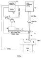
- FIG. 4 shows in block diagram form the overall system including the AFM.
- the chip 20 is mounted on a stage 30 for movement in the x-y plane.
- the AFM itself includes, in addition to the lens 27, a laser heterodyne system 31, the output of which is the z feedback signal to an amplifier 32 which provides an a.c. driving signal from generator 33 to the bimorphous crystal 26.
- the z feedback signal is also supplied to a microprocessor controller 34 which controls the application of the driving signal to the crystal 26, this being terminated with the z dimension has been determined. After the z dimension has been determined, the tip 16 is withdrawn to a predetermined distance above the bottom of the trench and moved relative to the trench in the x-y plane. This is accomplished by the controller 34 moving the stage 30.
- a feedback loop defined by the output signals from the sensors 171, 172, 173, and 174 to the controller 34 is used to control relative tip motion.
- the three dimensions determined in this fashion are output by the controller 34 to a suitable output device 35 with displays, prints and/or stores the data.
- a most valuable and important part of the invention is its ability to prevent "crashes" of the tip. "Crash” prevention is accomplished by the microprocessor controller 34 including a programmed routine which compares the absolute value of the voltage output from the sensors 171, 172, 173, and 174 with a predetermined threshold.
- the absolute valve of voltage is approximately linear function of tip deflection, and the threshold is selected to correspond to a tip deflection well within elastic limit of the tip 15.
- the routine simply compares each of the outputs of the sensors 171, 172, 173, and 174 with the predetermined threshold.
- An alternative, although more complex routine performs a simple trigonometric calculation on the two positive and two negative voltages from the sensors to resolve the direction of the tip deflection.
- Such a routine is part of the profiling computation performed by controller.
- the resolved absolute value of voltage amplitude is then compared to the threshold.
- the controller 34 stops the motion of the tip 15 relative to the sample being profiled and then backs the tip away from the surface feature with which the tip has come into contact.
- the preferred measurement regimen is illustrated in Figure 5.
- the tip 16 is first withdrawn by 20% of the trench depth, and the x and y coordinates determined for point A on side wall 22 and then point D on side wall 23. Then the tip 16 is withdrawn by 80% of the trench depth, and the x and y coordinates determined for point B on side wall 22 and then point C on side wall 23.
- the calculated width of the trench 21 is based on the root mean square of the width AD and the width BC.
Landscapes
- Physics & Mathematics (AREA)
- General Physics & Mathematics (AREA)
- Health & Medical Sciences (AREA)
- General Health & Medical Sciences (AREA)
- Nuclear Medicine, Radiotherapy & Molecular Imaging (AREA)
- Radiology & Medical Imaging (AREA)
- Chemical & Material Sciences (AREA)
- Engineering & Computer Science (AREA)
- Nanotechnology (AREA)
- Analytical Chemistry (AREA)
- Crystallography & Structural Chemistry (AREA)
- Length Measuring Devices With Unspecified Measuring Means (AREA)
Applications Claiming Priority (2)
| Application Number | Priority Date | Filing Date | Title |
|---|---|---|---|
| US07/999,059 US5321977A (en) | 1992-12-31 | 1992-12-31 | Integrated tip strain sensor for use in combination with a single axis atomic force microscope |
| US999059 | 1992-12-31 |
Publications (1)
| Publication Number | Publication Date |
|---|---|
| EP0608655A1 true EP0608655A1 (de) | 1994-08-03 |
Family
ID=25545847
Family Applications (1)
| Application Number | Title | Priority Date | Filing Date |
|---|---|---|---|
| EP93480202A Withdrawn EP0608655A1 (de) | 1992-12-31 | 1993-11-19 | In Sondenspitze integrierte Dehnungssensor für einachsiges Atomkraftmikroskop |
Country Status (3)
| Country | Link |
|---|---|
| US (2) | US5321977A (de) |
| EP (1) | EP0608655A1 (de) |
| JP (1) | JPH07104360B2 (de) |
Cited By (3)
| Publication number | Priority date | Publication date | Assignee | Title |
|---|---|---|---|---|
| EP0822387A3 (de) * | 1996-07-31 | 1999-01-13 | Carl Zeiss | Koordinatenmessgerät mit Kollisionsschutz |
| CN1320154C (zh) * | 2002-05-31 | 2007-06-06 | 中国科学院上海原子核研究所 | 在扫描探针显微镜悬臂及其针尖上沉积薄膜的方法 |
| CN102662085A (zh) * | 2010-11-23 | 2012-09-12 | F·J·吉斯布尔 | 用于表面的非接触轮廓分析的传感器 |
Families Citing this family (55)
| Publication number | Priority date | Publication date | Assignee | Title |
|---|---|---|---|---|
| DE69012555T2 (de) * | 1990-07-25 | 1995-04-06 | International Business Machines Corp., Armonk, N.Y. | Methode zur Herstellung von mikromechanischen Sensoren für AFM/STM/MFM-Profilometrie und mikromechanischer AFM/STM/MFM-Sensorkopf. |
| US5155361A (en) | 1991-07-26 | 1992-10-13 | The Arizona Board Of Regents, A Body Corporate Acting For And On Behalf Of Arizona State University | Potentiostatic preparation of molecular adsorbates for scanning probe microscopy |
| US5440920A (en) | 1994-02-03 | 1995-08-15 | Molecular Imaging Systems | Scanning force microscope with beam tracking lens |
| US5646339A (en) * | 1994-02-14 | 1997-07-08 | International Business Machines Corporation | Force microscope and method for measuring atomic forces in multiple directions |
| US5753814A (en) | 1994-05-19 | 1998-05-19 | Molecular Imaging Corporation | Magnetically-oscillated probe microscope for operation in liquids |
| US5515719A (en) | 1994-05-19 | 1996-05-14 | Molecular Imaging Corporation | Controlled force microscope for operation in liquids |
| US5866805A (en) | 1994-05-19 | 1999-02-02 | Molecular Imaging Corporation Arizona Board Of Regents | Cantilevers for a magnetically driven atomic force microscope |
| US5513518A (en) | 1994-05-19 | 1996-05-07 | Molecular Imaging Corporation | Magnetic modulation of force sensor for AC detection in an atomic force microscope |
| JP3229914B2 (ja) * | 1994-12-12 | 2001-11-19 | 日本電子株式会社 | 走査型プローブ顕微鏡 |
| WO1996028837A1 (en) * | 1995-03-10 | 1996-09-19 | Molecular Imaging Corporation | Hybrid control system for scanning probe microscopes |
| US5528033A (en) * | 1995-03-29 | 1996-06-18 | International Business Machines Corporation | Automatic surface profiling for submicron device |
| JP3608009B2 (ja) * | 1995-07-05 | 2005-01-05 | 株式会社ニコン | 原子間力顕微鏡 |
| US5705814A (en) * | 1995-08-30 | 1998-01-06 | Digital Instruments, Inc. | Scanning probe microscope having automatic probe exchange and alignment |
| US5630932A (en) * | 1995-09-06 | 1997-05-20 | Molecular Imaging Corporation | Tip etching system and method for etching platinum-containing wire |
| US5874668A (en) * | 1995-10-24 | 1999-02-23 | Arch Development Corporation | Atomic force microscope for biological specimens |
| US6118124A (en) * | 1996-01-18 | 2000-09-12 | Lockheed Martin Energy Research Corporation | Electromagnetic and nuclear radiation detector using micromechanical sensors |
| US5825670A (en) * | 1996-03-04 | 1998-10-20 | Advanced Surface Microscopy | High precison calibration and feature measurement system for a scanning probe microscope |
| US5644512A (en) * | 1996-03-04 | 1997-07-01 | Advanced Surface Microscopy, Inc. | High precision calibration and feature measurement system for a scanning probe microscope |
| US5700953A (en) * | 1996-04-03 | 1997-12-23 | University Of Utah Research Foundation | Method for mapping mechanical property of a material using a scanning force microscope |
| JP3290378B2 (ja) * | 1996-06-13 | 2002-06-10 | インターナショナル・ビジネス・マシーンズ・コーポレーション | Afm/stm形状測定のためのマイクロメカニカル・センサ |
| US6023338A (en) * | 1996-07-12 | 2000-02-08 | Bareket; Noah | Overlay alignment measurement of wafers |
| US5847569A (en) * | 1996-08-08 | 1998-12-08 | The Board Of Trustees Of The Leland Stanford Junior University | Electrical contact probe for sampling high frequency electrical signals |
| US5866806A (en) * | 1996-10-11 | 1999-02-02 | Kla-Tencor Corporation | System for locating a feature of a surface |
| US5773824A (en) * | 1997-04-23 | 1998-06-30 | International Business Machines Corporation | Method for improving measurement accuracy using active lateral scanning control of a probe |
| US5801381A (en) * | 1997-05-21 | 1998-09-01 | International Business Machines Corporation | Method for protecting a probe tip using active lateral scanning control |
| US5959200A (en) * | 1997-08-27 | 1999-09-28 | The Board Of Trustees Of The Leland Stanford Junior University | Micromachined cantilever structure providing for independent multidimensional force sensing using high aspect ratio beams |
| US5856967A (en) * | 1997-08-27 | 1999-01-05 | International Business Machines Corporation | Atomic force microscopy data storage system with tracking servo from lateral force-sensing cantilever |
| US5856617A (en) * | 1997-09-02 | 1999-01-05 | International Business Machines Corporation | Atomic force microscope system with cantilever having unbiased spin valve magnetoresistive strain gauge |
| US5949002A (en) * | 1997-11-12 | 1999-09-07 | Teradyne, Inc. | Manipulator for automatic test equipment with active compliance |
| US6050722A (en) * | 1998-03-25 | 2000-04-18 | Thundat; Thomas G. | Non-contact passive temperature measuring system and method of operation using micro-mechanical sensors |
| US6518570B1 (en) | 1998-04-03 | 2003-02-11 | Brookhaven Science Associates | Sensing mode atomic force microscope |
| US6000281A (en) * | 1998-05-04 | 1999-12-14 | Advanced Micro Devices, Inc. | Method and apparatus for measuring critical dimensions on a semiconductor surface |
| US6169281B1 (en) | 1998-07-29 | 2001-01-02 | International Business Machines Corporation | Apparatus and method for determining side wall profiles using a scanning probe microscope having a probe dithered in lateral directions |
| US6189374B1 (en) | 1999-03-29 | 2001-02-20 | Nanodevices, Inc. | Active probe for an atomic force microscope and method of use thereof |
| GB2348706B (en) | 1999-04-02 | 2003-09-24 | Mitutoyo Corp | Movement control mechanism of contact-type vibrating probe |
| EP1698905B9 (de) * | 1999-09-15 | 2012-01-18 | Capres A/S | Nanoantrieb für hochauflösende Positionierung und zur Positionierung einer Mehrpunktsonde |
| US6269685B1 (en) * | 1999-09-23 | 2001-08-07 | Ut Battelle, Llc | Viscosity measuring using microcantilevers |
| ATE323275T1 (de) | 2001-04-03 | 2006-04-15 | Saphirwerk Ind Prod | Verfahren zur bestimmung der grösse der deformation eines taststiftes |
| JP4656761B2 (ja) * | 2001-05-31 | 2011-03-23 | オリンパス株式会社 | Spmカンチレバー |
| WO2003083437A2 (en) * | 2002-03-22 | 2003-10-09 | Quantum Logic Devices, Inc. | Method and apparatus for identifying molecular species on a conductive surface |
| US8202440B1 (en) * | 2002-08-27 | 2012-06-19 | Kla-Tencor Corporation | Methods and apparatus for electron beam assisted etching at low temperatures |
| US6862924B2 (en) * | 2003-05-02 | 2005-03-08 | Board Of Trustees Operating Michigan State University | Augmenting reality system for real-time nanomanipulation using atomic force microscopy |
| US7552645B2 (en) * | 2003-05-07 | 2009-06-30 | California Institute Of Technology | Detection of resonator motion using piezoresistive signal downmixing |
| US7434476B2 (en) * | 2003-05-07 | 2008-10-14 | Califronia Institute Of Technology | Metallic thin film piezoresistive transduction in micromechanical and nanomechanical devices and its application in self-sensing SPM probes |
| EP1644473B1 (de) * | 2003-06-03 | 2014-01-15 | Cantimer Incorporated | Phasenänderungssensor |
| US20050092907A1 (en) * | 2003-11-04 | 2005-05-05 | West Paul E. | Oscillating scanning probe microscope |
| US7096711B2 (en) * | 2004-05-12 | 2006-08-29 | Veeco Instruments Inc. | Methods of fabricating structures for characterizing tip shape of scanning probe microscope probes and structures fabricated thereby |
| US7423264B2 (en) * | 2006-09-08 | 2008-09-09 | Kla-Tencor Technologies Corporation | Atomic force microscope |
| US7797991B2 (en) * | 2007-10-18 | 2010-09-21 | Texas Instruments Incorporated | Rocking Y-shaped probe for critical dimension atomic force microscopy |
| EP2278306A1 (de) * | 2009-07-13 | 2011-01-26 | Fei Company | Verfahren zur Untersuchung einer Probe |
| BG66424B1 (bg) | 2009-09-29 | 2014-03-31 | "Амг Технолоджи" Оод | Сензори за сканираща сондова микроскопия, метод за тримерно измерване и метод за получаване на такива сензори |
| JP6133678B2 (ja) | 2013-05-01 | 2017-05-24 | 株式会社ミツトヨ | 表面性状測定装置およびその制御方法 |
| US9909860B2 (en) * | 2015-04-15 | 2018-03-06 | General Electric Company | Systems and methods for monitoring component deformation |
| US9618334B2 (en) * | 2015-04-15 | 2017-04-11 | General Electric Company | Systems and methods for monitoring turbine component strain |
| CN111732073B (zh) * | 2020-06-18 | 2024-05-14 | 东北林业大学 | 一种基于针尖轨迹运动加工微纳复合结构的装置及方法 |
Citations (7)
| Publication number | Priority date | Publication date | Assignee | Title |
|---|---|---|---|---|
| GB2070249A (en) * | 1980-02-21 | 1981-09-03 | Rank Organisation Ltd | Contact-sensitive probe |
| JPS5733301A (en) * | 1980-08-08 | 1982-02-23 | Mitsutoyo Mfg Co Ltd | Copying probe for coordinate measuring machine |
| US4811594A (en) * | 1988-04-25 | 1989-03-14 | Battelle Memorial Institute | Topography sensor |
| DE3933575A1 (de) * | 1989-10-07 | 1991-04-18 | Hartmut Prof Dr Janocha | Tasteinrichtung |
| EP0483579A2 (de) * | 1990-10-31 | 1992-05-06 | International Business Machines Corporation | Nanometer Bereichssonde für ein auf atomaren Kräften beruhendes Mikroskop, und Verfahren zu dessen Herstellung |
| US5186041A (en) * | 1990-11-28 | 1993-02-16 | International Business Machines Corporation | Microprobe-based CD measurement tool |
| EP0536827A1 (de) * | 1991-09-27 | 1993-04-14 | International Business Machines Corporation | Kombiniertes Rasterkraftmikroskop und optisches metrologisches Gerät |
Family Cites Families (22)
| Publication number | Priority date | Publication date | Assignee | Title |
|---|---|---|---|---|
| CH643397A5 (de) * | 1979-09-20 | 1984-05-30 | Ibm | Raster-tunnelmikroskop. |
| US4888550A (en) * | 1981-09-14 | 1989-12-19 | Texas Instruments Incorporated | Intelligent multiprobe tip |
| US4506154A (en) * | 1982-10-22 | 1985-03-19 | Scire Fredric E | Planar biaxial micropositioning stage |
| US4724318A (en) * | 1985-11-26 | 1988-02-09 | International Business Machines Corporation | Atomic force microscope and method for imaging surfaces with atomic resolution |
| EP0262253A1 (de) * | 1986-10-03 | 1988-04-06 | International Business Machines Corporation | Mikromechanische Fühlervorrichtung für atomare Kräfte |
| DE3771711D1 (de) * | 1987-05-12 | 1991-08-29 | Ibm | Atomares kraeftemikroskop mit oscillierendem quarz. |
| JPS63304103A (ja) * | 1987-06-05 | 1988-12-12 | Hitachi Ltd | 走査表面顕微鏡 |
| EP0296262B1 (de) * | 1987-06-22 | 1991-08-28 | International Business Machines Corporation | Verfahren zur Oberflächenuntersuchung mit Nanometer- und Pikosekundenauflösung sowie Laserabgetastetes Rastertunnelmikroskop zur Durchführung des Verfahrens |
| JP2566794B2 (ja) * | 1987-10-15 | 1996-12-25 | セイコー電子工業株式会社 | 走査型トンネル顕微鏡の測定方法 |
| US4851767A (en) * | 1988-01-15 | 1989-07-25 | International Business Machines Corporation | Detachable high-speed opto-electronic sampling probe |
| JPH01224603A (ja) * | 1988-03-04 | 1989-09-07 | Agency Of Ind Science & Technol | 広範囲走査型トンネル顕微鏡 |
| US4924713A (en) * | 1988-03-14 | 1990-05-15 | Elco Co., Ltd. | Transducer to detect force which is applied to machine tool when machining workpiece and its attaching structure |
| JPH077654B2 (ja) * | 1988-04-01 | 1995-01-30 | 株式会社日立製作所 | 走査型電子顕微鏡 |
| JP2936545B2 (ja) * | 1988-06-24 | 1999-08-23 | 株式会社日立製作所 | 走査プローブ顕微鏡 |
| US5066358A (en) * | 1988-10-27 | 1991-11-19 | Board Of Trustees Of The Leland Stanford Juninor University | Nitride cantilevers with single crystal silicon tips |
| US4943719A (en) * | 1989-01-17 | 1990-07-24 | The Board Of Trustees Of The Leland Stanford University | Microminiature cantilever stylus |
| US4924091A (en) * | 1989-02-01 | 1990-05-08 | The Regents Of The University Of California | Scanning ion conductance microscope |
| EP0413041B1 (de) * | 1989-08-16 | 1992-07-15 | International Business Machines Corporation | Verfahren für die Herstellung mikromechanischer Messfühler für AFM/STM-Profilometrie und mikromechanischer Messfühlerkopf |
| EP0413040B1 (de) * | 1989-08-16 | 1992-12-16 | International Business Machines Corporation | Verfahren für die Herstellung ultrafeiner Siliziumspitzen für AFM/STM-Profilometrie |
| US5092163A (en) * | 1990-06-27 | 1992-03-03 | Young Russell D | Precision small scale force sensor |
| US5171992A (en) * | 1990-10-31 | 1992-12-15 | International Business Machines Corporation | Nanometer scale probe for an atomic force microscope, and method for making same |
| US5196701A (en) * | 1991-07-31 | 1993-03-23 | International Business Machines Corporation | High-resolution detection of material property variations |
-
1992
- 1992-12-31 US US07/999,059 patent/US5321977A/en not_active Expired - Lifetime
-
1993
- 1993-11-19 EP EP93480202A patent/EP0608655A1/de not_active Withdrawn
- 1993-11-24 US US08/157,800 patent/US5345816A/en not_active Expired - Fee Related
- 1993-12-09 JP JP5309377A patent/JPH07104360B2/ja not_active Expired - Fee Related
Patent Citations (7)
| Publication number | Priority date | Publication date | Assignee | Title |
|---|---|---|---|---|
| GB2070249A (en) * | 1980-02-21 | 1981-09-03 | Rank Organisation Ltd | Contact-sensitive probe |
| JPS5733301A (en) * | 1980-08-08 | 1982-02-23 | Mitsutoyo Mfg Co Ltd | Copying probe for coordinate measuring machine |
| US4811594A (en) * | 1988-04-25 | 1989-03-14 | Battelle Memorial Institute | Topography sensor |
| DE3933575A1 (de) * | 1989-10-07 | 1991-04-18 | Hartmut Prof Dr Janocha | Tasteinrichtung |
| EP0483579A2 (de) * | 1990-10-31 | 1992-05-06 | International Business Machines Corporation | Nanometer Bereichssonde für ein auf atomaren Kräften beruhendes Mikroskop, und Verfahren zu dessen Herstellung |
| US5186041A (en) * | 1990-11-28 | 1993-02-16 | International Business Machines Corporation | Microprobe-based CD measurement tool |
| EP0536827A1 (de) * | 1991-09-27 | 1993-04-14 | International Business Machines Corporation | Kombiniertes Rasterkraftmikroskop und optisches metrologisches Gerät |
Non-Patent Citations (2)
| Title |
|---|
| D.NYYSSONEN ET AL: "two-dimensional atomic force microprobe trench metrology system", JOURNAL OF VACUUM SCIENCE AND TECHNOLOGY: PART A., vol. 9, no. 6, November 1991 (1991-11-01), NEW YORK US, pages 3612 - 3616, XP000268571, DOI: doi:10.1116/1.585855 * |
| PATENT ABSTRACTS OF JAPAN vol. 6, no. 100 (P - 121) 9 June 1982 (1982-06-09) * |
Cited By (4)
| Publication number | Priority date | Publication date | Assignee | Title |
|---|---|---|---|---|
| EP0822387A3 (de) * | 1996-07-31 | 1999-01-13 | Carl Zeiss | Koordinatenmessgerät mit Kollisionsschutz |
| CN1320154C (zh) * | 2002-05-31 | 2007-06-06 | 中国科学院上海原子核研究所 | 在扫描探针显微镜悬臂及其针尖上沉积薄膜的方法 |
| CN102662085A (zh) * | 2010-11-23 | 2012-09-12 | F·J·吉斯布尔 | 用于表面的非接触轮廓分析的传感器 |
| CN102662085B (zh) * | 2010-11-23 | 2015-10-28 | F·J·吉斯布尔 | 用于表面的非接触轮廓分析的传感器 |
Also Published As
| Publication number | Publication date |
|---|---|
| JPH07104360B2 (ja) | 1995-11-13 |
| US5345816A (en) | 1994-09-13 |
| US5321977A (en) | 1994-06-21 |
| JPH06281658A (ja) | 1994-10-07 |
Similar Documents
| Publication | Publication Date | Title |
|---|---|---|
| US5321977A (en) | Integrated tip strain sensor for use in combination with a single axis atomic force microscope | |
| EP0584233B1 (de) | Submikron Spitzenanordnung mit gegenüberliegenden Spitzen | |
| US5345815A (en) | Atomic force microscope having cantilever with piezoresistive deflection sensor | |
| US6000280A (en) | Drive electrodes for microfabricated torsional cantilevers | |
| US5386720A (en) | Integrated AFM sensor | |
| US6196061B1 (en) | AFM with referenced or differential height measurement | |
| US6734425B2 (en) | Scanning probe system with spring probe and actuation/sensing structure | |
| US5283442A (en) | Surface profiling using scanning force microscopy | |
| US5929438A (en) | Cantilever and measuring apparatus using it | |
| US5329808A (en) | Atomic force microscope | |
| US5920067A (en) | Monocrystalline test and reference structures, and use for calibrating instruments | |
| EP0536827A1 (de) | Kombiniertes Rasterkraftmikroskop und optisches metrologisches Gerät | |
| Lee et al. | Submicron Si trench profiling with an electron‐beam fabricated atomic force microscope tip | |
| JP5254509B2 (ja) | カンチレバーおよびシールドを備えた静電気力検出器 | |
| KR19990029072A (ko) | 내부 원자 측정 방법 | |
| US5929643A (en) | Scanning probe microscope for measuring the electrical properties of the surface of an electrically conductive sample | |
| US6552556B1 (en) | Prober for electrical measurement of potentials in the interior of ultra-fine semiconductor devices, and method of measuring electrical characteristics with said prober | |
| US5186041A (en) | Microprobe-based CD measurement tool | |
| EP0843175B1 (de) | Rastersondenmikroskop und Signalverarbeitungsgerät | |
| EP1135665B1 (de) | Messungen zwischen langgestreckten leitern unter verwendung des tunnelstroms | |
| Lebrasseur et al. | A new characterization tool for vertical profile measurement of high-aspect-ratio microstructures | |
| JP2002156409A (ja) | 集積回路における電気信号の検出のための測定ゾンデ及びこの測定ゾンデの使用法及びこの測定ゾンデの製造方法及びこの測定ゾンデによる測定システム | |
| JPH1038916A (ja) | プローブ装置及び微小領域に対する電気的接続方法 | |
| JP2001108605A (ja) | 走査型プローブ顕微鏡用カンチレバー及びその製造方法、並びに走査型プローブ顕微鏡及び表面電荷測定顕微鏡 | |
| JPH06258072A (ja) | 圧電体薄膜評価装置、原子間力顕微鏡 |
Legal Events
| Date | Code | Title | Description |
|---|---|---|---|
| PUAI | Public reference made under article 153(3) epc to a published international application that has entered the european phase |
Free format text: ORIGINAL CODE: 0009012 |
|
| AK | Designated contracting states |
Kind code of ref document: A1 Designated state(s): DE FR GB |
|
| 17P | Request for examination filed |
Effective date: 19941021 |
|
| 17Q | First examination report despatched |
Effective date: 19960319 |
|
| STAA | Information on the status of an ep patent application or granted ep patent |
Free format text: STATUS: THE APPLICATION IS DEEMED TO BE WITHDRAWN |
|
| 18D | Application deemed to be withdrawn |
Effective date: 19961001 |