EP0609074B1 - Zusammenbaustruktur einer Flachtyp-Anordnung - Google Patents
Zusammenbaustruktur einer Flachtyp-Anordnung Download PDFInfo
- Publication number
- EP0609074B1 EP0609074B1 EP94300593A EP94300593A EP0609074B1 EP 0609074 B1 EP0609074 B1 EP 0609074B1 EP 94300593 A EP94300593 A EP 94300593A EP 94300593 A EP94300593 A EP 94300593A EP 0609074 B1 EP0609074 B1 EP 0609074B1
- Authority
- EP
- European Patent Office
- Prior art keywords
- flexible wiring
- panel
- peripheral portion
- terminals
- terminal
- Prior art date
- Legal status (The legal status is an assumption and is not a legal conclusion. Google has not performed a legal analysis and makes no representation as to the accuracy of the status listed.)
- Expired - Lifetime
Links
Images

















Classifications
-
- G—PHYSICS
- G02—OPTICS
- G02F—OPTICAL DEVICES OR ARRANGEMENTS FOR THE CONTROL OF LIGHT BY MODIFICATION OF THE OPTICAL PROPERTIES OF THE MEDIA OF THE ELEMENTS INVOLVED THEREIN; NON-LINEAR OPTICS; FREQUENCY-CHANGING OF LIGHT; OPTICAL LOGIC ELEMENTS; OPTICAL ANALOGUE/DIGITAL CONVERTERS
- G02F1/00—Devices or arrangements for the control of the intensity, colour, phase, polarisation or direction of light arriving from an independent light source, e.g. switching, gating or modulating; Non-linear optics
- G02F1/01—Devices or arrangements for the control of the intensity, colour, phase, polarisation or direction of light arriving from an independent light source, e.g. switching, gating or modulating; Non-linear optics for the control of the intensity, phase, polarisation or colour
- G02F1/13—Devices or arrangements for the control of the intensity, colour, phase, polarisation or direction of light arriving from an independent light source, e.g. switching, gating or modulating; Non-linear optics for the control of the intensity, phase, polarisation or colour based on liquid crystals, e.g. single liquid crystal display cells
- G02F1/133—Constructional arrangements; Operation of liquid crystal cells; Circuit arrangements
- G02F1/1333—Constructional arrangements; Manufacturing methods
- G02F1/1345—Conductors connecting electrodes to cell terminals
- G02F1/13452—Conductors connecting driver circuitry and terminals of panels
-
- H—ELECTRICITY
- H10—SEMICONDUCTOR DEVICES; ELECTRIC SOLID-STATE DEVICES NOT OTHERWISE PROVIDED FOR
- H10W—GENERIC PACKAGES, INTERCONNECTIONS, CONNECTORS OR OTHER CONSTRUCTIONAL DETAILS OF DEVICES COVERED BY CLASS H10
- H10W70/00—Package substrates; Interposers; Redistribution layers [RDL]
- H10W70/60—Insulating or insulated package substrates; Interposers; Redistribution layers
- H10W70/67—Insulating or insulated package substrates; Interposers; Redistribution layers characterised by their insulating layers or insulating parts
- H10W70/688—Flexible insulating substrates
-
- G—PHYSICS
- G02—OPTICS
- G02F—OPTICAL DEVICES OR ARRANGEMENTS FOR THE CONTROL OF LIGHT BY MODIFICATION OF THE OPTICAL PROPERTIES OF THE MEDIA OF THE ELEMENTS INVOLVED THEREIN; NON-LINEAR OPTICS; FREQUENCY-CHANGING OF LIGHT; OPTICAL LOGIC ELEMENTS; OPTICAL ANALOGUE/DIGITAL CONVERTERS
- G02F1/00—Devices or arrangements for the control of the intensity, colour, phase, polarisation or direction of light arriving from an independent light source, e.g. switching, gating or modulating; Non-linear optics
- G02F1/01—Devices or arrangements for the control of the intensity, colour, phase, polarisation or direction of light arriving from an independent light source, e.g. switching, gating or modulating; Non-linear optics for the control of the intensity, phase, polarisation or colour
- G02F1/13—Devices or arrangements for the control of the intensity, colour, phase, polarisation or direction of light arriving from an independent light source, e.g. switching, gating or modulating; Non-linear optics for the control of the intensity, phase, polarisation or colour based on liquid crystals, e.g. single liquid crystal display cells
- G02F1/133—Constructional arrangements; Operation of liquid crystal cells; Circuit arrangements
- G02F1/136—Liquid crystal cells structurally associated with a semi-conducting layer or substrate, e.g. cells forming part of an integrated circuit
- G02F1/1362—Active matrix addressed cells
- G02F1/136259—Repairing; Defects
- G02F1/136272—Auxiliary lines
-
- H—ELECTRICITY
- H05—ELECTRIC TECHNIQUES NOT OTHERWISE PROVIDED FOR
- H05K—PRINTED CIRCUITS; CASINGS OR CONSTRUCTIONAL DETAILS OF ELECTRIC APPARATUS; MANUFACTURE OF ASSEMBLAGES OF ELECTRICAL COMPONENTS
- H05K1/00—Printed circuits
- H05K1/02—Details
- H05K1/14—Structural association of two or more printed circuits
-
- H—ELECTRICITY
- H05—ELECTRIC TECHNIQUES NOT OTHERWISE PROVIDED FOR
- H05K—PRINTED CIRCUITS; CASINGS OR CONSTRUCTIONAL DETAILS OF ELECTRIC APPARATUS; MANUFACTURE OF ASSEMBLAGES OF ELECTRICAL COMPONENTS
- H05K3/00—Apparatus or processes for manufacturing printed circuits
- H05K3/36—Assembling printed circuits with other printed circuits
- H05K3/361—Assembling flexible printed circuits with other printed circuits
-
- H—ELECTRICITY
- H10—SEMICONDUCTOR DEVICES; ELECTRIC SOLID-STATE DEVICES NOT OTHERWISE PROVIDED FOR
- H10W—GENERIC PACKAGES, INTERCONNECTIONS, CONNECTORS OR OTHER CONSTRUCTIONAL DETAILS OF DEVICES COVERED BY CLASS H10
- H10W72/00—Interconnections or connectors in packages
- H10W72/071—Connecting or disconnecting
- H10W72/072—Connecting or disconnecting of bump connectors
- H10W72/07251—Connecting or disconnecting of bump connectors characterised by changes in properties of the bump connectors during connecting
-
- H—ELECTRICITY
- H10—SEMICONDUCTOR DEVICES; ELECTRIC SOLID-STATE DEVICES NOT OTHERWISE PROVIDED FOR
- H10W—GENERIC PACKAGES, INTERCONNECTIONS, CONNECTORS OR OTHER CONSTRUCTIONAL DETAILS OF DEVICES COVERED BY CLASS H10
- H10W72/00—Interconnections or connectors in packages
- H10W72/20—Bump connectors, e.g. solder bumps or copper pillars; Dummy bumps; Thermal bumps
-
- Y—GENERAL TAGGING OF NEW TECHNOLOGICAL DEVELOPMENTS; GENERAL TAGGING OF CROSS-SECTIONAL TECHNOLOGIES SPANNING OVER SEVERAL SECTIONS OF THE IPC; TECHNICAL SUBJECTS COVERED BY FORMER USPC CROSS-REFERENCE ART COLLECTIONS [XRACs] AND DIGESTS
- Y10—TECHNICAL SUBJECTS COVERED BY FORMER USPC
- Y10T—TECHNICAL SUBJECTS COVERED BY FORMER US CLASSIFICATION
- Y10T29/00—Metal working
- Y10T29/49—Method of mechanical manufacture
- Y10T29/49002—Electrical device making
- Y10T29/49117—Conductor or circuit manufacturing
- Y10T29/49124—On flat or curved insulated base, e.g., printed circuit, etc.
- Y10T29/49155—Manufacturing circuit on or in base
Definitions
- the present invention relates to a flat panel device and method for assembling the same. More specifically, the invention relates to a flat panel device including a panel having electrode terminals disposed on a peripheral portion thereof, such as liquid crystal, EL, plasma, and other panels.
- a liquid crystal panel is described here.
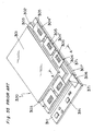
- a liquid crystal panel 320 is in general so structured that liquid crystals 321 are sealed in between a pair of glass substrates 301, 302 and a large number of electrode terminals 303 are disposed on a peripheral portion of one glass substrate 302.
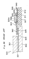
- Fig. 56 shows a section as viewed along the line A - A' in Fig. 55.
- the liquid crystal panel 320 has on a peripheral portion thereof: flexible wiring boards 304, 304', ...
- the common wiring board 307 has, on its one surface, a bus line (circuit wiring) 371, and electrode terminals 372 electrically conducting with the bus line 371 and corresponding to the flexible wiring boards 304, 304', ..., respectively.
- the flexible wiring board 304 has a wiring layer, which includes output terminals 342 and an input terminal 306, provided on a base material surface 340 having flexibility.
- the drive IC 305 is connected to the wiring layer by bump electrodes 305a, 305b (numeral 396 denotes resin).
- the glass substrate 302 and the common wiring board 307 are juxtaposed with the electrode terminals 303, 372 faced upward. Then the electrode terminals 303 and 372 are electrically connected to the output terminals 342 and input terminal 306 of the flexible wiring board 304 by means of an anisotropic conductive material 395 or solder (not shown), respectively. Also, as shown in Fig. 55, one end of the connector 308 is connected to the bus line 371 of the common wiring board 307, while the other end of the connector 308 is connected to a signal feed terminal (not shown) of the control board 311.
- a signal is fed to the bus line 371 of the common wiring board 307 from the control board 311 via the connector 308.
- the signal is inputted to the drive IC 305 of the flexible wiring boards 304, 304', ....
- the signal outputted by the drive IC 305 is applied to pixels through the output terminals 342 and the electrode terminals 303.
- the liquid crystal panel 320 is driven.
- the above-described conventional assembling structure has both the common wiring board 307 and the control board 311 disposed and spaced from each other on side portions of the liquid crystal panel 320, thus inevitably resulting in a rather large size module.
- the common wiring board 307 and the control board 311 are provided, the resulting module is increased in weight, making a difficulty for weight reduction.
- the number of parts is increased so that the material cost is also increased.
- the manufacturing man-hours required is increased, disadvantageously causing higher cost.
- the present invention has been developed with a view to substantially solving the above described disadvantages and aims to provide a structure of, and method for assembling, a flat panel device by which a panel having electrode terminals disposed on a peripheral portion thereof, typified by liquid crystal panels, can be assembled with small size, light weight, low cost, and high reliability.
- a control signal is fed to the substrate wiring on the panel from an external control board via a connector or the like.
- the control signal is inputted to the drive IC from the first junction terminal via the input terminal of the flexible wiring board.
- a signal outputted by the drive IC is fed to the inside of the panel via the output terminals of the flexible wiring board and the electrode terminals of the peripheral portion of the panel.
- the panel is driven.
- the control signal is passed sequentially through the board circuit wiring and the further output terminal of the flexible wiring board, the second junction terminal and the substrate circuit wiring of the peripheral portion of the panel, and thus fed to the first junction terminal corresponding to another flexible wiring board adjacent to the flexible wiring board.
- the signal is inputted to the drive IC from the first junction terminal via the input terminal of the adjacent flexible wiring board.
- a signal outputted by the drive IC is fed to the inside of the panel via the output terminals of the adjacent flexible wiring board and the electrode terminals of the peripheral portion of the panel. In this way, the control signal is fed to the electrode terminals corresponding to an adjacent flexible wiring board one after another.
- the common wiring board which would normally be disposed sideward of the panel in the prior art, is omitted. Accordingly, the module can be reduced in size compared with the prior art. Also the number of parts is reduced so that the weight of the module is reduced. Such reduction in the number of parts allows a reduction in material cost. Yet, the first junction terminal, electrode terminals, and second junction terminal of the peripheral portion of the panel are collectively connected to the input terminal, output terminals, and further output terminal of the flexible wiring board by means of, for example, an anisotropic conductive material. Also, there is no step of connecting the flexible wiring boards and a common wiring board (the control board is connected to the further wiring of the peripheral portion of the panel via a connector as in the prior art). Accordingly, the man-hours required are reduced so that the cost lowers.
- the module is less affected by any external force so that the rate of occurrence of defects lowers, accompanied by other advantages. As a result, the module reliability is enhanced.
- any flexible wiring board on which an IC has proved to be, or become, defective after assembling can be easily exchanged for a new one without the need of removing adhesive or for other process steps.
- a prober terminal for performance tests can be put in contact with the terminals through the portion where the base material surface has been removed, while the flexible wiring board is connected to the peripheral portion of the panel. As a result, performance tests for the panel and the drive ICs can be easily performed.
- the width of the peripheral portion of the panel is required only to be equivalent to the portions carrying the terminals, so that the width of the peripheral portion of the panel can be designed to be narrow. As a result, the module size can be further reduced.
- the width of the peripheral portion of the panel is required only to be equivalent to the portions carrying corresponding to the terminals so that the width of the peripheral portion of the panel can be designed narrow. As a result, the module size can be further reduced.
- the respective drive IC When the respective drive IC is mounted on that portion of the corresponding wiring board which is bent, the extent to which the flexible wiring board projects outwardly of the peripheral portion of the panel is reduced by an extent of the width of the drive IC. As a result, the module size can be further reduced.
- a control board for feeding a signal for driving the panel is electrically connected to the flexible wiring boards, in the arrangement on the flexible wiring boards there is provided a fourth junction terminal leading to the further output terminal via a third wiring; in an arrangement on one surface of the control board a signal feed terminal for feeding a signal for driving the panel is provided in a position corresponding to the fourth junction terminal of the flexible wiring boards; and the control board is overlaid on the flexible wiring boards so that the fourth junction terminal of the flexible wiring boards is electrically connected to the signal feed terminal of the control board.
- a signal is fed from the signal feed terminal of the control board to the fourth junction terminal of the flexible wiring board.
- This signal is inputted from the fourth junction terminal to the drive IC sequentially via the third wiring, the further output terminal, the board wiring, and the input terminal.
- a signal outputted by the drive IC is fed to the inside of the panel via the output terminals of the flexible wiring board and the electrode terminals of the peripheral portion of the panel (direct route).
- the panel is driven.
- the signal can be fed to the panel through a following indirect route.
- the signal branched by the further output terminal of the flexible wiring board passed sequentially through the second junction terminal and substrate wiring leading thereto of the peripheral portion of the panel, and thus fed to the first junction terminal corresponding to an adjacent flexible wiring board. Then the signal is inputted to the drive IC from the first junction terminal via the input terminal of the adjacent flexible wiring board.
- a signal outputted by the drive IC is fed to the inside of the panel via the output terminals of the adjacent flexible wiring board and the electrode terminals of the peripheral portion of the panel. In this way, the signal is fed to the electrode terminals corresponding to an adjacent flexible wiring board one after another.
- the signal is fed from the control board to the flexible wiring boards by a direct route, i.e. a shortest route as required. Accordingly, the wire resistance is reduced.
- the fourth junction terminal of part of the plurality of flexible wiring boards are not connected to the signal feed terminal of the control board, the number of connecting points between the flexible wiring boards and control board is reduced. As a result, the man-hours required and accordingly manufacturing cost is further reduced.
- the fourth junction terminal of the flexible wiring board may be connected to the signal feed terminal of the control board at a comer portion of the peripheral portion of the panel, while the fourth junction terminal of the flexible wiring boards is not connected to the signal feed terminal of the control board at places other than the corner portion.
- the flexible wiring boards are prepared as provided with a fourth junction terminal, and the fourth junction terminal is cut off and removed before starting the assembly. In such a case, design cost for the flexible wiring boards will never increase.
- the module size is further reduced.
- the module When the control board is overlaid on the peripheral portion of the panel directly or via a spacer and assembled integrally therewith, the module is increased in strength with its reliability enhanced. Also, it is no longer needed to provide any auxiliary reinforcement member for assembling the panel and the control board, so that the module can be designed for small size and light weight.
- the module size is further reduced.
- any flexible wiring board on which an IC has proved to be, or has become defective after assembling is mounted can be easily exchanged for a new one.
- a method for assembling a flat panel device in which a panel has a plurality of electrode terminals disposed along a peripheral portion of one surface thereof, a plurality of flexible wiring boards which each have a wiring layer on a flexible base material and on which a drive IC for driving the panel is mounted, are electrically connected to the electrode terminals of the panel, and a circuit wiring provided on the panel for transferring an externally fed signal is electrically connected to the flexible wiring boards
- the method for assembling the flat type device comprising the steps of: (A) providing, on the peripheral portion of the panel and for each flexible wiring board a corresponding, first junction terminal sharing the same layer with the electrode terminals and disposed spaced to one side of a group of the electrode terminals corresponding to that flexible wiring board in a direction extending along the peripheral portion of the panel, and providing a said circuit wiring for connection to each said first junction terminal of the flexible wiring boards, said circuit wiring being disposed in the region of a row along which said electrode and first junction
- the connecting process between the flexible wiring boards and the control board is reduced in burden to a level similar to or less than the connecting process for the common wiring board in the prior art.
- the connecting process for the connector is entirely obviated. Accordingly, the total man-hours required are reduced compared with the prior art. As a result, the cost lowers.
- the control board When the control board is overlaid directly or via a spacer on the surface of the peripheral portion of the panel opposite to the surface on which the electrode terminals are provided, and when the flexible wiring boards are wound around a peripheral portion of the panel and the control board, and further when a clip made of a shape memorizing member having a U shape in section is provided to pinch the peripheral portion of the panel and the control board on outside of the flexible wiring boards so that a group of the terminals on the peripheral portion of the panel and the corresponding terminals on the flexible wiring boards are pressed together, then the module size is further reduced. Yet, the terminals can be easily connected to each other so that the assembly work is facilitated.
- connection between the panel and the flexible wiring boards and connection between the flexible wiring boards and the control board can be achieved simultaneously and collectively. Accordingly, the man-hours required are reduced so that the manufacturing cost lowers.
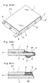
- Fig. 1 is a perspective view of the liquid crystal module which is not an embodiment of the present invention.
- a liquid crystal panel 20 has liquid crystals 21 (see Fig. 4 (b)) sealed between a pair of glass substrates 1, 2.
- Flexible wiring boards 4, 4', ... each having a drive IC 5 for driving the liquid crystal panel 20 mounted thereon are attached on the peripheral portion of one glass substrate 2.
- Fig. 2 is a plan view of the peripheral portion of the liquid crystal panel 20 of Fig. 1, while Fig. 3 is a sectional view taken along the line B - B' of Fig. 2 in the arrow direction.
- a bus line 73 as a circuit wiring is provided at a layer below the electrode terminals 3.
- the bus line 73 extends along the peripheral portion of the panel and is electrically insulated from the electrode terminals 3 with an insulating layer 9 interposed therebetween (a base coat 11 having insulating property is provided between the bus line 73 and the glass substrate 2).
- the insulating layer 9 has through holes 74 formed at specified points thereon.
- a junction terminal 45 is also provided so as to lead to the bus line 73 via the through holes 74.
- the junction terminal 45 shares the same layer with the electrode terminals 3 do.
- the flexible wiring board 4 is rectangular in shape, having an input terminal 44 and output terminals 42 of a strip shape provided along one side line of the rectangle on one surface of the flexible wiring board 4.
- the drive IC 5 is mounted along a side line opposite to that for the input terminal 44 and the output terminals 42 by means of gang bond (collective thermal press bonding) or use of solder or conductive paste. It is noted that the line 43 has a capacitor 55 for use of signal adjustment connected thereto. Adjacent to the flexible wiring board 4 is provided a flexible wiring board 4' having the completely same arrangement as in the board 4.
- the junction terminal 45 and the electrode terminals 3 are aligned with the input terminal 44 and the output terminals 42, respectively, in one-to-one correspondence. Then, as shown in Fig. 3, the junction terminal 45 and the electrode terminals 3 are pressed or thermally press bonded with the input terminal 44 and the output terminals 42 by means of an anisotropic conductive material 95. Thereby, the junction terminal 45 and the electrode terminals 3 are collectively electrically connected to the input terminal 44 and the output terminals 42, respectively. Also, as shown in Fig.
- a drive-use signal is fed to the bus line 73 of the peripheral portion of the panel via the connector 8 from external.
- This signal is inputted to the drive IC 5 sequentially through the junction terminal 45, the input terminal 44 of the flexible wiring board 4, and the line 43 as shown in Fig. 2.
- a signal outputted by the drive IC 5 is fed to pixels (not shown) of the liquid crystal panel 20 sequentially through the line 41, the output terminals 42, and the electrode terminals 3 of the peripheral portion of the panel.
- the liquid crystal panel 20 is driven.
- this liquid crystal module is provided with no common wiring board 307 that would be disposed on one side of the glass substrate 2 in the prior art (see Fig. 55), the size of the module can be reduced compared with the prior art. Also, the number of parts can be reduced so that the weight of the module can also be reduced. Such reduction in the number of parts allows a reduction in material cost. Yet, connection of the terminals 45, 3 of the peripheral portion of the panel and the terminals 44, 42 of the flexible wiring board can be accomplished only by a one-time connecting process. As a result, the man-hour required can be reduced compared with the prior art, leading to a cost reduction.
- portions where the peripheral portion of the liquid crystal panel 20 overlaps with the flexible wiring boards 4, 4', ... as well as the drive IC 5 may be firmly coated with an epoxic, ultraviolet-setting type protective resin 6 with high rigidity, which would tend to crack in the conventional structure so that it could not be used.
- an epoxic, ultraviolet-setting type protective resin 6 with high rigidity which would tend to crack in the conventional structure so that it could not be used.
- a silicone series, soft resin may be used to coat the portions as in the prior art.
- Figs 5 (a), (b) show an example in which the protective resin 6 is applied to the module of Fig. 1, while Figs.
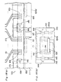
- Fig. 7 is a perspective view of a liquid crystal module which is an embodiment of the present invention.
- a liquid crystal panel 120 has liquid crystals 121 (see Fig. 9) sealed between a pair of glass substrates 101, 102.
- Flexible wiring boards 104, 104', 104'', 104S, and 104S' each having a drive IC 105 for driving the liquid crystal panel 120 mounted thereon are attached on the peripheral portion of one glass substrate 102.
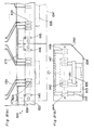
- Figs. 8 (a) and (b) are plan views of the peripheral portion of the liquid crystal panel 120 and the flexible wiring board 104, respectively.
- a first junction terminal 145 on the peripheral portion of the liquid crystal panel 120 (glass substrate 102), there are disposed a first junction terminal 145, electrode terminals 103, and a second junction terminal 146 at a specified pitch in a plurality in series, all of which terminals are strip shaped and share the same layer.
- the electrode terminals 103 lead to pixels (not shown) inside the panel via lines 131.
- a first circuit wiring 173, constituting the panel wiring referred to in the claims is provided on the panel's inner side of the junction terminals 146, 145.
- the first circuit wiring 173 extends along the peripheral portion of the panel, electrically connecting the junction terminal 146 and the junction terminal 145 to each other.
- the lines 131 and the first circuit wiring 173 are coated with an insulating layer 109.
- the flexible wiring board 104 is of an approximately rectangular shape, having a wiring layer including an input terminal 144, output terminals 142, and a third junction terminal 148, referred to in the claims as the further output terminal, provided to a flexible base material surface 140.
- the input terminal 144, the output terminals 142, and the third junction terminal 148 are all strip-shaped and provides at places corresponding to the terminals 145, 103, and 146, respectively, of the peripheral portion of the panel on the rear side of the flexible wiring board 104.
- a second circuit wiring 147, constituting the board wiring referred to in the claims, for connecting the input terminal 144 to the third junction terminal 148 is provided so as to extend along the row of the input terminal 144, output terminals 142, and the third junction terminal 148.
- the input terminal 144 and the output terminals 142 lead to the drive IC 105 via a line 143 and a line 141, respectively.
- the first junction terminal 145, the electrode terminals 103, and the second junction terminal 146 are aligned with the input terminal 144, the output terminals 142, and the third junction terminal 148, respectively, in one-to-one correspondence.
- the first junction terminal 145, the electrode terminals 103, and the second junction terminal 146 are thermally press bonded with the input terminal 144, the output terminals 142, and the third junction terminal 148 by means of an anisotropic conductive material 195.
- the various terminals are collectively electrically connected to their corresponding ones.
- the flexible wiring board 104 is overlapped with the peripheral portion of the panel in such a way that the row of the input terminal 144, the output terminals 142, and the third junction terminal 148 is located outside the second circuit wiring 147.
- the anisotropic conductive material 195 may be provided in such an extent as to cover the dimensions of the various terminals, or otherwise may be provided over the outer whole range of the insulating layer 109.
- solder, photo-setting resins, or other connecting materials may be used instead of the anisotropic conductive material 195. In this way, as shown in Fig.
- the signal is branched at the first junction terminal 145 so as to be fed to the first junction terminal 145 of another flexible wiring board 104' adjacent to the flexible wiring board 104, sequentially through the second circuit wiring 147 and third junction terminal 148 of the flexible wiring board 104, the second junction terminal 146 of the peripheral portion of the panel, and the first circuit wiring 173 leading thereto. Then the signal is inputted from the first junction terminal 145 via the input terminal of the flexible wiring board 104' to the drive IC 105. A signal outputted by this drive IC 105 is fed to the inside of the panel via the output terminals of the flexible wiring board 104' and the electrode terminals 103 of the peripheral portion of the panel.
- the signal is fed to the electrode terminals 103 of the flexible wiring boards 104, 104', ... adjacent to one another, in turn.
- the signal is similarly fed to the electrode terminals 103 of the flexible wiring boards 104S, 104S' adjacent to one another on another side of the liquid crystal panel 120 (Fig. 7).
- this liquid crystal module is provided with no common wiring board 307 that would be disposed sideward of the panel in the prior art (see Figs. 55 and 56), the size of the module can be reduced compared with the prior art. Also, the number of parts can be reduced so that the weight of the module can also be reduced. Such reduction in the number of parts allows a reduction in material cost. Yet, the first junction terminal 145, electrode terminals 103, and second junction terminal 146 of the peripheral portion of the panel are connected to the input terminal 144, output terminals 142, third junction terminal 148 of the flexible wiring board 104 collectively by means of the anisotropic conductive material 195. Further, the connection process of the flexible wiring boards 104, ...
- the control board is connected to the first circuit wiring of the peripheral portion of the panel via a connector as in the prior art.
- the man-hour required can be reduced compared with the prior art, leading to a cost reduction.
- a higher reliability also can be attained.
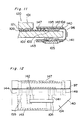
- Figs. 10 and 11 show a modification example of the above-described liquid crystal module.
- a slit 96 is provided at a portion of the base material surface 140 where the flexible wiring boards 104, ... are wound around the peripheral portion of the panel, in the direction along the peripheral portion. Further, the flexible wiring boards 104, ... are connected to the peripheral portion of the panel and thereafter bent by their portion projecting sideward of the peripheral portion of the liquid crystal panel 120 (glass substrate 102) so as to be wound around the peripheral portion of the panel. Thereby, the size of the module can be further reduced. It is noted that the provision of the slit 96 makes the flexible wiring boards 104, ... easy to bend, facilitating the assembling.
- a clip made of a shape memorizing alloy or shape memory plastics having a U shape in section may also be used to pinch the peripheral portion of the panel on the outer peripheral side of the flexible wiring boards 104, ... so that the various terminals involved are press bonded. As a result, the terminals can be easily connected to their corresponding ones.
- a slit 97 may be provided at a portion of the base material surface 140 corresponding to a gap between the row of the input terminal 144, the output terminals 142, and the third junction terminal 148 of the flexible wiring board 4 and the second circuit wiring 147, so that it ranges along the gap.
- the slit 97 since the slit 97 is in proximity to the row of the terminals 144, 142, and 148, any excessive portions of the anisotropic conductive material 195 will easily flow out uniformly among the terminals through the slit 97 when the flexible wiring board 104 is connected to the peripheral portion of the panel, as shown in Fig. 13. As a result, a stabler reliability of the connecting portions is attained.
- base material surface 140 of the flexible wiring board 104 corresponding to the input terminal 144, output terminals 142, and the third junction terminal 148 are removed and an opening 98 is provided.
- a prober terminal for performance tests can be thrown in contact with the input terminal 144, output terminals 142, or third junction terminal 148 of the flexible wiring board 104. Therefore, performance tests for the liquid crystal panel 120 and the drive ICs can be easily performed.
- a portion of the flexible wiring board 104 corresponding to the second circuit wiring 147 is bent 90 degrees to 180 degrees with respect to the portions of the input terminal 144, the output terminals 142, and the third junction terminal 148.
- the width of the peripheral portion of the panel is required only to be equivalent to the terminals 144, 142, and 148 so that the width of the peripheral portion of the panel can be designed narrow. As a result, the module size can be further reduced.
- the flexible wiring board 104 is overlaid on the peripheral portion of the panel so that the row of the input terminal 144, the output terminals 142, and the third junction terminal 148 is located inwardly of the second circuit wiring 147, and that a portion of the flexible wiring board 104 opposite to the second circuit wiring 147 is bent 90 degrees to 180 degrees with respect to the portions corresponding to the terminals 144, 142, and 148.
- numeral 109 denotes a rod-like member for giving the bent portion 100 of the flexible wiring board 104 a curvature. In such a case, as in the case of Fig.
- the flexible wiring board may be a front-and-rear double-layer wiring type with bumps. This makes it possible to design other different compact modules.
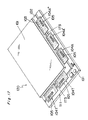
- Fig. 17 is a perspective view of a liquid crystal module which is another an embodiment according to the present invention.
- a liquid crystal panel 120 has liquid crystals 121 (see Fig. 22) sealed between a pair of rectangular glass substrates 101, 102.
- Five flexible wiring boards 104A, 104A', 104A'', 104T, and 104T' each having a drive IC 105 for driving the liquid crystal panel 120 mounted thereon are attached on the peripheral portion of one glass substrate 102.
- An L-shaped control board 111 for feeding signals for driving the liquid crystal panel 120 is provided along the peripheral portion of the liquid crystal panel 120 (numeral 191 denotes an electronic component).
- Figs. 18 (a) and (b) are plan views of the peripheral portion of the liquid crystal panel 120 and the flexible wiring board 104A, respectively.
- a first junction terminal 145 on the peripheral portion of the liquid crystal panel 120 (glass substrate 102), there are disposed a first junction terminal 145, electrode terminals 103, and a second junction terminal 146 at a specified pitch in a plurality in series, all of which terminals are strip shaped and share the same layer.
- the electrode terminals 103 lead to pixels (not shown) inside the panel via lines 131.
- a first circuit wiring 173 is provided on the panel's inner side of the junction terminals 146, 145.
- the first circuit wiring 173 extends along the peripheral portion of the panel, electrically connecting the junction terminal 146 and the junction terminal 145 to each other.
- the lines 131 and the first circuit wiring 173 are covered with an insulating layer 109.
- the flexible wiring board 104A is of an approximately rectangular shape, having a wiring layer including an input terminal 144, output terminals 142, a third junction terminal 148 provided to a base material surface 140 with a flexibility.
- the input terminal 144, the output terminals 142, and the third junction terminal 148 are all strip-shaped and provided at places corresponding to the terminals 145, 103, and 146, respectively, of the peripheral portion of the panel on the rear side of the flexible wiring board 104A.
- a second circuit wiring 147 for connecting the input terminal 144 to the third junction terminal 148 is provided so as to extend along the row of the input terminal 144, output terminals 142, and a third junction terminal 148.
- the input terminal 144 and the output terminals 142 lead to the drive IC 105 via a line 143 and a line 141, respectively.
- the first junction terminal 145, the electrode terminals 103, and the second junction terminal 146 are aligned with the input terminal 144, the output terminals 142, and the third junction terminal 148, respectively, in one-to-one correspondence.
- the first junction terminal 145, the electrode terminals 103, and the second junction terminal 146 are thermally press bonded with the input terminal 144, the output terminals 142, and the third junction terminal 148 by means of an anisotropic conductive material 195.
- the various terminals are collectively electrically connected to their corresponding ones.
- the flexible wiring board 104A is overlapped with the peripheral portion of the panel in such a way that the row of the input terminal 144, the output terminals 142, and the third junction terminal 148 is located outside the second circuit wiring 147.
- the anisotropic conductive material 195 may be provided in such an extent as to cover the dimensions of the various terminals, or otherwise may be provided over the outer whole range of the insulating layer 109. Also, solder or other connecting materials may be used instead of the anisotropic conductive material 195. In this way, as shown in Fig.
- a signal is fed from the signal feed terminal 151 of the control board 111 to the fourth junction terminal 149 of the flexible wiring board 104A.
- This signal is inputted to the drive IC 105 from the fourth junction terminal 149 sequentially through the third circuit wiring 150, the third junction terminal 148, the second circuit wiring 147, the input terminal 144, and the line 143, as shown in Fig. 18 (b).
- a signal outputted by the drive IC 105 is fed to pixels (not shown) of the liquid crystal panel 120 sequentially through the line 141 and output terminals 142 of the flexible wiring board 104A, the electrode terminals 103 of the peripheral portion of the panel, and the lines 131 (direct route).
- the liquid crystal panel 120 is driven at a shortest route and with less wire resistance.
- this liquid crystal module is provided with no common wiring board 307 or connector that would be disposed sideward of the panel in the prior art (see Figs. 55 and 56), the size of the module can be reduced compared with the prior art. Also, the number of parts can be reduced so that the weight of the module can also be reduced. Such reduction in the number of parts allows a reduction in material cost. Yet, the first junction terminal 145, electrode terminals 103, and second junction terminal 146 of the peripheral portion of the panel are connected to the input terminal 144, output terminals 142, third junction terminal 148 of the flexible wiring board 104A, ... collectively by means of the anisotropic conductive material 195. Further, the connection process of the flexible wiring boards 104A, ...
- control board 111 can be achieved by such less work as to be equivalent to the connection process for the common wiring board of the prior art.
- the connection process for the connector can be completely omitted.
- the man-hour required can be reduced as a whole, compared with the prior art, leading to a cost reduction.
- a higher reliability also can be attained.
- the control board 111 may be a board made of hard type glass epoxy, or otherwise of thin, soft type polyimide or polyester. The latter case allows further reduction in thickness and weight of the module.
- Figs. 19 to 21 each show a modification example of the above-described liquid crystal module.
- the fourth junction terminal 149 of the flexible wiring board 104T' is not connected to the signal feed terminal of a control board 111A (the control board 111A is so designed that its shorter side line of an L-shape become short for weight reduction, as compared with the control board 111 shown in Fig. 17).
- the control board 111A is so designed that its shorter side line of an L-shape become short for weight reduction, as compared with the control board 111 shown in Fig. 17).
- the drive-use signal is fed to the portions of the peripheral portion of the panel corresponding to the flexible wiring boards 104A, 104A', 104A'', and 104T via the aforementioned direct route, while the signal is fed to the portion of the peripheral portion of the panel corresponding to the flexible wiring board 104T' via the aforementioned indirect route.
- the fourth junction terminal 149 and the third circuit wiring 150 of the flexible wiring boards 104A, 104A', and 104T'' have been cut off and removed together with the base material surface 140 (a control board 111B is so designed that both its longer and shorter side lines of L-shape become short for weight reduction).
- a control board 111B is so designed that both its longer and shorter side lines of L-shape become short for weight reduction.
- the number of points where the flexible wiring board is connected to the control board 111B can be reduced, so that the man-hour required can be reduced with further cost reduction.
- the fourth junction terminal 149 and the third circuit wiring 150 may be cut off and removed before starting the assembling.
- the aforementioned drive-use signal is fed to the portions of the peripheral portion of the panel corresponding to the flexible wiring boards 104A, 104T via the aforementioned direct route, while the signal is fed to the portions of the peripheral portion of the panel corresponding to the flexible wiring board 104A', 104A'', and 104T'' via the aforementioned indirect route.
- the portions of the flexible wiring boards 104A', 104A'', and 104T', which are not connected to the control board 111B, that project sideward of the peripheral portion of the panel are bent so as to be wound around the peripheral portion of the panel.
- the number of points where the flexible wiring boards are connected to the control board 111B can be reduced.
- the module size can be further reduced.
- the control board 111 is mounted on a surface opposite to the surface on which the electrode terminals 103 of the peripheral portion of the panel are provided in such a way that the control board 111 is bonded by the adhesive 112 so as not to project sideward of the peripheral portion of the panel.
- the flexible wiring board 104A is bent so as to be wound around the peripheral portions of the liquid crystal panel 120 and the control board 111.
- the module size can be further reduced.
- the strength of the module can be increased so that its reliability can be enhanced and that the module can be designed to be lightweight.
- spacers 113, 113 may be provided between the glass substrate 102 and the control board 111 to ensure a clearance for the electronic component 191.
- a clip 110 made of a shape memorizing alloy or shape memory plastics having a U shape is used to pinch the peripheral portion of the panel and the control board 111 on the outer periphery of the flexible wiring board 104A, thereby pressing the corresponding terminals.
- Numeral 114 denotes a buffer material.
- the anisotropic conductive material or the like can be omitted between the corresponding terminals, facilitating the connection of the terminals.
- the liquid crystal panel 120 can be easily assembled.
- any defective drive ICs 105 if any can be easily replaced with new ones.
- the control board 111 does not project sideward of the liquid crystal panel 120, so that the module size can be further reduced.
- the strength of the module can be increased so that its reliability can be enhanced and that the module can be designed lightweight.
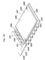
- Fig. 30 is a perspective view of a liquid crystal display device 221, which is another an embodiment according to the present invention.
- Fig. 31 is a plan view of the liquid crystal display device 221 around a flexible wiring board 230.
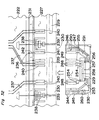
- Fig. 32 is an exploded perspective view of the liquid crystal display device 221 around the flexible wiring board.
- Fig. 33 is a sectional view as viewed along the cutting-plane line X33 - X33 of Fig. 31.
- Fig. 34 is a sectional view as viewed along the cutting-plane line X34 - X34 of Fig. 31.
- the liquid crystal display device 221 is taken as an example.
- the embodiments of the present invention can be applied to not only the liquid crystal display device 221 but also a wide variety of matrix-driven display devices including the EL display devices or plasma display devices.
- a drive IC 229 for driving the liquid crystal display device 221 is mounted on a peripheral portion 227 of one glass substrate 222 other than the range over which the glass substrate 222 overlaps the other glass substrate 223, there are mounted ten flexible wiring boards 230.
- a peripheral portion 227 is an L-shaped region extending along adjoining two sides of the glass substrate 222.
- the flexible wiring board 230 has an insulating film 243 (see Fig. 33) made of an electrically insulating material such as polyimide resin and polyester resin. On this insulating film 243, various terminals and wiring lines later described are formed.
- Common lines 231 for feeding signals or power to be fed in common to the flexible wiring boards 230 are formed continuously over the range over which the plurality of flexible wiring boards 230 are arranged on the peripheral portion 227.
- a signal or drive-use power to be fed in common to the flexible wiring boards 230 is fed to the common lines 231 from a control board 232 via a connector 233.
- the display device 221 is comprised of the display panel 228, the plurality of flexible wiring boards 230, and the control board 232.
- an insulating film 234 is formed on the glass substrate 222 of the display panel 228 by forming a Ta 2 O 5 film as an example.
- the plurality of common lines 231 are formed from such a material as ITO, Ta, Ti, Mo, Cu, Au, Al, and Ag paste, in a single-layer or multi-layer structure so as to be 50 nm or more in thickness, a few ⁇ m - a few mm in line width, and 0.1 ⁇ / ⁇ - several 100's ⁇ / ⁇ in resistance at a length ranging over approximately the entire length of the peripheral portion 227.
- an insulating film 235 is formed from such a material as SiN, SiO 2 , Ta 2 O 5 , or polyimide so as to have a plurality of through holes 236.
- signal lines 237 for example, each connected to a group of pixels corresponding to each row of the whole pixels arrayed in a matrix within the display section 226; and signal-use junction common lines 238 and power-use junction common lines 239 each having a length ranging between opposing terminals of adjacent flexible wiring boards 230 on the peripheral portion 227.
- the junction common lines 238, 239 are formed from such a material as ITO, Ta, Ti, Mo, Cu, Au, Al, and Ag paste in a single-layer or multilayer structure so as to be 50 nm or more in thickness, a few ⁇ m - a few mm in line width, and 0.1 ⁇ / ⁇ - several 100's ⁇ / ⁇ in resistance.
- the junction common lines 238, 239 as shown in Figs. 31 and 32, are arrayed in a direction perpendicular to the direction in which the plurality of flexible wiring boards 230 are arrayed on the peripheral portion 227 (lateral direction in Figs. 31 and 32). Rectangular connecting portions 240 are formed at an equal pitch at end portions of the signal lines 237.
- each lead-in line 242 is connected to a common line 231 via a through hole 236 of insulating film 235 and the other end of which extends toward an end of the peripheral portion 227.
- the end portion of each lead-in line 242 is connected to rectangular connecting portions 241 arrayed along the aforementioned array direction on the peripheral portion 227.
- An insulating film 263 is formed so as to cover the common lines 231 and the lead-in lines 242 as described above.
- output terminals 246, 247 for outputting signals of the same type as those inputted to the input terminals 244, 245 are arrayed in a direction perpendicular to the aforementioned array direction, at an end portion of the flexible wiring boards 230 opposite to the end portion where the input terminals 244, 245 are located, in the same arrayed state as in the input terminals 244, 245.
- the input terminals 244, 245 and the output terminals 246, 247 are formed from such a material as Sn- or Au-plated Cu and aluminum so as to be 10 - 60 ⁇ m in thickness and a few ⁇ m - a few mm in line width.
- accommodating hole 250 for accommodating the IC 229 are formed at positions away from the end portions of the flexible wiring boards 230.
- the IC 229 within the accommodating holes 250 is firmly coated with a protective resin layer 251, for example, of epoxy resin.
- the IC 229 is provided with a plurality of electrode bumps 252.
- a plurality of connecting lines 253, 254, 255 are formed for connecting the input terminals 244, 245, the electrode terminals 248, 249, and the output terminals 246, 247 to their corresponding electrode bumps 252 of the IC 229.
- alignment marks 290 are provided at positions corresponding to some of the electrode terminals 249.
- a connecting line 256 is formed for connecting the input terminal 245 directly to the output terminal 247, while a branch line 257 is formed for connecting the connecting line 256 to its corresponding electrode bump 252 of the IC 229.
- Some signals inputted from the input terminals 244 to one flexible wiring board 230 are to be transferred to another adjacent flexible wiring board 230.
- a plurality of internal lines 258 for connecting at the inside of the IC 229 the input-use connecting line 253 directly to an output-use connecting line 291 (see Fig. 32) in correspondence to the signal to be transferred are formed within the IC 229.
- a chip capacitor 260 for signal adjustment is connected to the connecting line 256 and part of the connecting lines 253. Thereby, any differences in display grade among the ICs 229 of the flexible wiring boards 230 are reduced.
- connection between the above-described display panel 228 and the flexible wiring boards 230 is achieved by using an anisotropic conductive film 259.
- Fig. 35 is a flow chart showing the process of manufacturing the display device 221, which process is an embodiment according to the present invention.
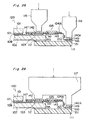
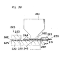
- Fig. 36 is a sectional view showing the manufacturing process.
- the connecting portions 240, 241, the electrode terminals 248, 249, the junction common lines 238, 239 and input/output terminals 244, 245, 246, 247 of one flexible wiring board 230 located at its both ends in the array direction are aligned for each flexible wiring board 230 in one-to-one correspondence, respectively.
- the display panel 228, on which the aligned flexible wiring boards 230 are mounted are heated by a thermal press head 261 having a single or plurality of press portions 262 which is shown in Fig. 36 and which have such a shape as to press the connecting portions to the display panel 228 of each flexible wiring board 230.
- thermal press bonding is achieved, as shown in Fig. 36, between the connecting portions 240, 241 and the electrode terminals 248, 249, and between the junction common lines 238, 239 and the input/output terminals 244, 245, 246, 247 located at both ends in the array direction of one flexible wiring board 230.
- opposing electrodes of the connecting portions 240, 241, the terminals 244, 245, 246, 247, 248, 249, and the junction common lines 238, 239 can be electrically connected collectively.
- the display device 221 can be provided in smaller size, thinner thickness, and less weight. Further, the display device 221 is less affected by any external force by virtue of its reduced size, so that the reliability of the display device 221 can be improved.
- a plurality of flexible wiring boards 230 which have the same wiring pattern and which serve for, for example, driving scanning lines of the display device 221 are connected to the display panel 228 along one side of the display device 221.
- flexible wiring boards 230 which have a wiring pattern different from that of the foregoing flexible wiring boards 230 and which serve for, for example, driving data lines of the display device 221 are connected to the display panel 228.
- a control board 232 for feeding signals for driving the display device 221 is connected to the common lines 231 and the junction common lines 238, 239 via the connector 233.
- a drive-use signal is fed from the control board 232 to the common lines 231 and the junction lines 238 of the peripheral portion 227 of the display device 221 via the connector 233.
- the signal drives the IC 229 from the connecting portions 241 and terminals 244, 245, as shown in Figs. 31 and 32, via the connecting lines 253, 251 of the flexible wiring boards 230, while output signals of the IC 229 are fed to the pixel electrodes (not shown) of the display device 221 via the connecting lines 254 and the electrode terminals 248. Thereby, the display device 221 is driven.
- the above drive-use signal is branched by the junction common line 238 and fed to the input terminals 244 of a flexible wiring board 230 adjacent to the foregoing flexible wiring board 230 via the input terminals 244 and connecting line 253 of the flexible wiring board 230, lower lines or internal lines 258 of the IC 229, the connecting lines 291, the output terminals 246, and the junction common lines 238. Then the signal is fed from the input terminals 244 via the connecting lines 253 of the adjacent flexible wiring boards 230 to the drive IC 229. A signal outputted by the drive IC 229 is fed to the inside of the display section 226 of the display panel 228 via the output terminals 246 of the flexible wiring boards 230 and the connecting portions 240 of the peripheral portion 227.
- the above drive-use signals are fed to the connecting portions 240 of a plurality of the flexible wiring boards 230 mounted on one side of the peripheral portion 227 of the liquid crystal display device 221.
- the same drive-use signals are similarly fed also to the connecting portions 240 of the flexible wiring boards 230 (see Fig. 30) mounted on another side of the liquid crystal display device.
- the liquid crystal display device 221 is provided with no common wiring board 307 (see Figs. 55 and 56) that would be disposed sideward of the liquid crystal display device 301 in the prior art, the size of the liquid crystal display device 221 can be reduced, so that the liquid crystal display device 221 can be offered in less thickness and weight. This also allows cost reduction of the liquid crystal display device 221.
- connection between the junction lines 238, 239 of the peripheral portion 227 of the liquid crystal display device 221 and the input terminals 244, 245 of the flexible wiring boards 230, connection between the output terminals 246, 247 of the flexible wiring boards 230 and the junction lines 238, 239, and connection between the connecting portions 240, 241 and the electrode terminals 248, 249 of the flexible wiring boards 230 are achieved collectively by means of the anisotropic conductive film 259.
- the connecting process for manufacturing the liquid crystal display device 221 can be reduced, so that the rate of occurrence of any defectives in the connecting process is reduced, and that the production yield in the assembling process is improved. Also, a cost reduction can be expected in terms of the manufacturing process.
- a signal to be transferred from one to another among the flexible wiring boards 230 is transferred via the junction common lines 238, 239 and the connecting line 256 within the flexible wiring boards 230. Accordingly, wire resistance involved in the transfer of a signal can be reduced more than when the signal is transferred by using only the common lines 231 formed on the peripheral portion 227 of the display panel 228 by the thin-film technique. Also, the input terminals 244, 245, output terminals 246, 247, and electrode terminals 248, 249 of the flexible wiring boards 230 can be increased in line width and, besides, the junction common lines 238, 239, connecting portions 240, 241 of the display panel 228 can also be increased in line width. As a result, connection resistance that results when the flexible wiring boards 230 are mounted onto the display panel 228 can be reduced.
- the flexible wiring boards 230 of this embodiment it is also possible that a resin having an electrical insulation property is applied to the surface on which the input terminals 244, 245, thereby forming an insulating coat, so that the plurality of input terminals 244, 245, terminals 248, 249, connecting terminals 253, 254, 255, 291, 256, and output terminals 246, 247 are increased in reliability on their mutual electrical insulation.
- Fig. 37 is a plan view of a flexible wiring board 230a which is a modification example of the flexible wiring boards 230 of the foregoing embodiment, for use in the liquid crystal display device 221.
- this modification flexible wiring board 230a corner portions at both ends of a side of an insulating film 243 (see Figs. 33, 34) of the flexible wiring boards 230 of the foregoing embodiment, the side being opposed to the display panel 228, have been cut out to form cutouts 266.
- the signal inputted to one of the plurality of input terminals 244 formed on the flexible wiring board 230 is a signal of a first type that should be inputted to the IC 229 mounted on the flexible wiring board 230
- the first type signal is inputted from an input terminal 244a through a connecting line 253 to the IC 229.
- the signal is processed at the inside of the IC 229, where a different waveform signal is generated and then passed through a connecting line 291 and a terminal 246a, thus fed to an adjacent flexible wiring board 230.
- the signal to be inputted as above is a signal of a second type that, for example, is inputted to the IC 229 and should be transferred to another adjacent flexible wiring board 230 without being changed in signal waveform
- the second type signal is inputted to an input terminal 244b that is connected to the IC 229 via the connecting line 253 and besides connected directly to an output terminal 246b corresponding to the input terminal 244b via the connecting line 256.
- the flexible wiring board 230a as described above is mounted to the display panel 228 in the same assembling process as in the foregoing embodiment. In this process, clearances due to the cutouts 266 are formed between a plurality of adjacent flexible wiring boards 230a mounted on the display panel 228. Through these clearances, as shown in Fig. 37, part of the input terminals 244b, 244c, part of the connecting lines 256, and part of the output terminals 246b, 246c are exposed to outside. Accordingly, when this flexible wiring board 230a is used, the clearances are coated with an insulating film made of such a material as SiN and polyimide, as an example, on the panel side.
- Fig. 38 is a perspective view of a liquid crystal display device 221a which is a further embodiment of the present invention.
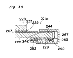
- Fig. 39 is a sectional view of this embodiment.
- the liquid crystal display device 221a of this embodiment is similar to the liquid crystal display device 221 of the foregoing embodiment of figure 30, where corresponding parts are designated by same reference numerals.
- the plurality of flexible wiring boards 230 are connected to the peripheral portion 227 of the display panel 228. Thereafter, portions of the flexible wiring boards 230 that project outward of the peripheral portion 227 of the display panel 228 are bent so as to be wound around the peripheral portion 227 of the display panel 228, as shown in Figs. 38 and 39. By this bending process, the display panel 228 of the liquid crystal display device 221 is pinched by the flexible wiring boards 230 at their peripheral portion 227.
- the size of the liquid crystal display device 221a can be further reduced by the bending extent of the flexible wiring boards 230.
- a clip 267 made of a shape memorizing alloy or shape memory plastics having a U shape in section is used to pinch the display panel 228 by its peripheral portion 227 on the outer peripheral side of the bent flexible wiring boards 230 and, in this state, the junction lines 238, 239 and the connecting portions 240, 241 and their corresponding input terminals 244, 245, output terminals 246, 247, and terminals 248, 249 are press bonded with each other.
- the terminals for connection of the display panel 228 and the flexible wiring boards 230 can be connected each other simply and firmly.
- a spacer 292 is mounted to the flexible wiring boards 230.
- the same effects as described in the foregoing embodiment can be achieved. Besides, the reliability of connection between the display panel 228 and the plurality of flexible wiring boards 230 can be further improved.
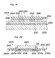
- Fig. 40 is a plan view of a liquid crystal display device 221b which is a further embodiment of the present invention.
- Fig. 41 is a sectional view taken along the line X41 - X41 of Fig. 40.
- Fig. 42 is a sectional view taken along the line X42 - X42 of Fig. 40.
- This embodiment is similar to the foregoing embodiment of figure 30 and 31, where corresponding parts are designated by same reference numerals.
- the third remarkable point of the present embodiment is that the input terminals 244, 245, the output terminals 246, 247, and the electrode terminals 248, 249 in the first embodiment are arrayed in the second direction (up and down direction in Figs. 32 and 40) perpendicular to the first direction (right and left direction in Figs. 31 and 40) in which the lead-in lines 242 in the display panel 228 are arrayed.
- the length of the flexible wiring boards 230 along the first direction can be reduced, compared with the case where the electrode terminals 248, 249 are arrayed in the first direction as in the first embodiment.
- the liquid crystal display device 221 can be reduced in size.
- Fig. 43 is a plan view of a liquid crystal display device 221c which is a further fourth embodiment of the present invention.
- Fig. 44 is a sectional view taken along the line X44 - X44 of Fig. 43. This embodiment is similar to the previous embodiment, where corresponding parts are designated by same reference numerals.
- the remarkable point of the present embodiment is that there are formed a plurality of connecting lines 269 for connecting all the input terminals 244, 245 and all the output terminals 246, 247 of the flexible wiring boards 230 separately and directly in the structure of the foregoing embodiment.
- the connecting lines 269 are formed of such a material as Sn- or Au-plated Cu.
- One end of the connecting lines 269 is connected to the input terminals 244, 245, while the other end is connected to the output terminals 246, 247.
- An intermediate portion of the connecting lines 269 is, as shown in Fig. 44, fixed at a position around the accommodating hole 250 which accommodates the ICs 229 and which is formed in the base material 243 of the flexible wiring boards 230, by using a protective resin 251 in the flexible wiring boards 230.
- In the connecting lines 269 underneath the IC 229 there are formed connecting portions 270 to be connected to a plurality of electrode bumps 252 of the IC 229.
- the same effects as described in the foregoing embodiments can be achieved. Further, since the present embodiment allows the internal lines 258 for use of signal transmission of the ICs 229, which have been used in the previous embodiment, to be omitted, the IC 229 can be simplified in their internal structure and therefore reduced in size. This makes it possible to downsize the structure of the liquid crystal display device 221c.
- Fig. 45 is a sectional view showing the structure of a first modification example of the above-described embodiment, or a sectional view of the display panel 228 taken at a cutting position corresponding to Fig. 44.
- the IC 229 to be mounted on the flexible wiring boards 230 may be also arranged on the side of the flexible wiring boards 230 on which the connecting lines 269 are formed.
- Fig. 46 is a sectional view showing the structure of a second modification example of the present embodiment, or a sectional view of the display panel 228 taken at a position corresponding to Fig. 44.
- the accommodating holes 250 are not formed in the flexible wiring boards 230 of this modification example.
- the connecting lines 269 are formed on the base material 243 of the flexible wiring boards 230.
- the IC 229 to be mounted are arranged on the base material 243 in the flexible wiring boards 230, for example, on the side on which the connecting lines 269 of the flexible wiring boards 230 are formed. Even in such a modification example, the effects of the present embodiment can be achieved.
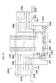
- Fig. 47 is a plan view of a liquid crystal display device 221 which is a further embodiment of the present invention.
- Fig. 48 is a sectional view taken along the line X48 - X48 of Fig. 47. This embodiment is similar to the figure 40 embodiment, where corresponding parts are designated by same reference numerals.
- the flexible wiring boards 230 have the accommodating holes 250 formed therein, where the IC 229 to be mounted are accommodated in the accommodating holes 250 and fixed to the base material 243 of the flexible wiring boards 230 by the protective layer 251.
- the input terminals 244, 245 and the output terminals 246, 247 are formed on one surface of the base material 243.
- a plurality of connecting lines 271 are formed on the base material 243 so as to directly connect the input terminals 244, 245 and the output terminals 246, 247 in such a wiring state as to detour the accommodating holes 250.
- the connecting lines 271 are made of such a material as Sn- or Au-plated Cu.
- the chip capacitor 260 is connected to specified connecting lines 271 such as one corresponding to the power line.
- connecting lines 271 should be connected to not only the output terminals 246, 247 but also the electrode bumps 252 of the IC 229.
- a plurality of connecting lines 272 for connection between the connecting lines 271 and the electrode bumps 252 of the IC 229 are formed on the base material 243 in order to connect the connecting lines 271 to the IC 229. More specifically, an insulating film 273 is formed on a region where at least the connecting lines 272 are coated. The insulating film 273 has through holes 274 formed at positions corresponding to the connecting lines 272. Over the range of the insulating film 273 and the range of the base material 243, the plurality of connecting lines 271 are formed. The connecting lines 271 are electrically connected to their corresponding connecting lines 272 via the through holes 274 of the insulating film 273. In such an embodiment, the same effects as described in the foregoing embodiments can be achieved.
- a plurality of output terminals 246, 247 and a plurality of connecting lines 276 one end of which is connected to the output terminals 246, 247 and extends along the second direction (up and down direction of Fig. 49) and the other end of which is positioned in an extension of the first direction (right and left direction of Fig. 49) of the IC 229.
- bypass wirings 277 are formed separately between the through holes 278 corresponding to the connecting lines 271 on the signal output side and the through holes 278 corresponding to the connecting lines 271 on the signal output side.
- the bypass wirings 277 are made of such a material as Sn- or Au-plated Cu.
- the same effects as described in the foregoing embodiments can be achieved.
- the connecting lines 271, 271, the connecting lines 272, and the bypass wirings 277 are formed so as to be separated between both surfaces of the base material 243 and overlaid on each other. Accordingly, wiring density in the both surfaces of the flexible wiring boards 230 can be increased so that the flexible wiring boards 230 and the liquid crystal display device 221e can be designed for smaller size.
- Fig. 51 is a sectional view of a liquid crystal display device 221f which is a further embodiment according to the present invention.
- Fig. 52 is a plan view of the liquid crystal display device 221f. This embodiment is similar to the figure 30, 31 embodiment, where corresponding parts are designated by same reference numerals.
- the region where the common lines 231 are formed is made larger than the peripheral portion 227 of the display panel 228. This allows the area of the peripheral portion 227 to be reduced and therefore the liquid crystal display device 221f to be downsized. Otherwise, arrangement density of the common lines 231 can be lowered, so that the common lines 231 can be prevented from shortcircuiting among themselves or from occurrence of insulating failures. As a result, the reliability of the liquid crystal display device 221f can be improved. Moreover, the production yield of the liquid crystal display device 221f can be improved at the same time.
- some of the common lines 231 are arranged by making the use of the region of the display panel 228 inner than the sealant 225 except the region of the opposite electrodes 280, whereby the line width of the common lines 231 is widened and the resistance is lowered. As a result, time delay of a signal transferred through the common lines 231 is reduced.
- the signal transferred when being an image signal, can be prevented from inclusion of noise that might cause the waveform of the image signal to be deformed undesirably.
- the resulting display image can be prevented from occurrence of failures.
- Fig. 53 is a sectional view of a liquid crystal display device 221g which is a further embodiment according to the present invention.
- Fig. 54 is a plan view of the liquid crystal display device 221g. This embodiment is similar to the foregoing Fig.52 embodiment, where corresponding parts are designated by same reference numerals.
- the liquid crystal display device 221g of this embodiment has nearly the same structure as the liquid crystal display device 221f.
- This embodiment is characterized in the arrangement of common lines 231 and common lines 231a.
- the plurality of common lines 231, 231a are formed over the entire regions including a range on the glass substrate 222 outer than the sealant 225, a region coated with the sealant 225, and a region inner than the sealant 225 and yet around the peripheral portion of the display section 226.
- these common lines 231, 231a some of the common lines 231a are provided as signal lines which transfer signals that do not easy pick up noise of the opposite electrodes 280 such as a clock signal.
- the common lines 231, 231a are coated with an insulating film 283 such as a known orientation film or protective film (passivation film).
- the common lines 231 may be formed on the glass substrate 222. In such an embodiment, the same effects as described in the seventh embodiment can be achieved.
- the connecting material for electrically connecting the display panel 228 to the flexible wiring boards 230 is not limited to the anisotropic conductive film 259. Instead, connection techniques other than the anisotropic conductive film 259 may be used, such as connection by the use of solder or photo-setting resins and clip press bonding.
Landscapes
- Physics & Mathematics (AREA)
- Nonlinear Science (AREA)
- Mathematical Physics (AREA)
- Chemical & Material Sciences (AREA)
- Crystallography & Structural Chemistry (AREA)
- General Physics & Mathematics (AREA)
- Optics & Photonics (AREA)
- Devices For Indicating Variable Information By Combining Individual Elements (AREA)
- Liquid Crystal (AREA)
- Combinations Of Printed Boards (AREA)
Claims (28)
- Flachtafelvorrichtung in welcher eine elektrisch steuerbare Flachtafel (120; 228) ein Feld von Elektrodenanschlüssen (103; 240) einschließt, die an und beabstandet entlang dem Umfangsabschnitt eines Substrats (102; 222) der Tafel bereitgestellt sind, und in welcher zumindest erste und zweite Verdrahtungsplatinen (104; 104A; 230), wobei jede eine Treiber-IC (105; 229) zum elektrischen Steuern der Tafel, einen Eingangsanschluss (144; 244, 245), der mit der jeweiligen Treiber-IC gekoppelt ist, und Ausgangsanschlüsse (142; 248), die mit der Treiber-IC gekoppelt sind, einschließt, nebeneinander an dem Umfangsabschnitt angebracht sind, wobei die Ausgangsanschlüsse (142; 248) elektrisch mit den Elektrodenanschlüssen (103; 240) verbunden sind, wobei die Vorrichtung eine Einrichtung zum Leiten von Steuersignalen für eine Versorgung zu den Treiber-IC's in einer Richtung entlang des Umfangsabschnitts einschließt, dadurch gekennzeichnet, dass die ersten und zweiten Verdrahtungsplatinen jeweils einen weiteren Ausgangsanschluss (148; 246, 247) aufweisen, der mit dem Eingangsanschluss (144; 244, 245) davon mittels eines Steuersignalpfads verbunden ist, der zumindest eine Platinenverdrahtung (147; 253, 255; 253, 291; 256; 253a; 269; 271) auf der Platine einschließt, wobei die Steuersignal-Leitungseinrichtung die Steuersignalpfade auf den Platinen einschließt, und wobei eine leitfähige Kopplungseinrichtung (145, 146, 173; 238, 239), die auf dem Substrat (102; 222) gehalten ist, den weiteren Ausgangsanschluss (148; 246, 247) der ersten Verdrahtungsplatine mit dem Eingangsanschluss (144; 244, 245) der zweiten Verdrahtungsplatine koppelt, wodurch der Leitungspfad für die Steuersignale zu der zweiten Verdrahtungsplatine teilweise auf der Tafel und teilweise auf der ersten Verdrahtungsplatine liegt.
- Flachtafelvorrichtung nach Anspruch 1, einschließend zumindest eine weitere Verdrahtungsplatine, die an dem Umfangsabschnitt angebracht ist, wobei die jeweiligen leitfähigen Kopplungseinrichtungen (145, 146, 173; 238, 239), die die jeweiligen Sätze der weiteren Ausgangs- und Eingangsanschlüsse benachbarter Paare von Verdrahtungsplatinen (104/104', 104'/104"; 104A/104A', 104A'/104A"; 230/230) koppelt, auf dem Umfangsabschnitt des Substrats gebildet sind und elektrisch voneinander isoliert sind.
- Flachtafelvorrichtung nach Anspruch 1 oder 2, dadurch gekennzeichnet, dass der Steuersignalpfad die Platinenverdrahtung (253, 255; 253, 291; 253a, 255a) und eine interne Leitung (258) der Treiber-IC einschließt.
- Flachtafelvorrichtung nach Anspruch 1 oder 2, dadurch gekennzeichnet, dass der Steuersignalpfad nur die Platinenverdrahtung (147; 256; 269; 271) einschließt.
- Flachtafelvorrichtung nach einem der voranstehenden Ansprüche, dadurch gekennzeichnet, dass
die Verdrahtungsplatinen flexibel sind und jeweils ein flexibles Grundmaterial (140; 243), auf welches die jeweilige Treiber-IC (105; 229) angebracht ist, und eine Verdrahtungsschicht, die den Eingangsanschluss (144; 244, 245), die Ausgangsanschlüsse (142; 248) und den weiteren Ausgangsanschluss (148; 246, 247) einschließt, umfassen;
die leitfähigen Kopplungseinrichtungen, die auf dem Substrat gehalten sind, umfassen:bezüglich jeder Verdrahtungsplatine einen ersten Verbindungsanschluss (145; 248), beabstandet zu einer Seite einer Gruppe der Elektrodenanschlüsse (103; 240), die dieser Verdrahtungsplatine entsprechen, in der Richtung entlang des Umfangsabschnitts, und einen zweiten Verbindungsanschluss (146; 238), beabstandet zu der anderen Seite der Gruppe von Elektrodenanschlüssen in der Richtung, wobei die ersten und zweiten Verbindungsanschlüsse die gleiche Schicht mit den Elektrodenanschlüssen teilen, undeine Substratverdrahtung (173; 238), die den zweiten Verbindungsanschluss, der einer der Verdrahtungsplatinen zugeordnet ist, mit dem ersten Verbindungsanschluss, der einer benachbarten Verdrahtungsplatine zugeordnet ist, verbindet, wobei das Substrat in dem Bereich einer Zeile angeordnet ist, entlang welcher die Elektrodenanschlüsse, die ersten Verbindungsanschlüsse und die zweiten Verbindungsanschlüsse ausgerichtet sind;der Eingangsanschluss (144; 244), die Ausgangsanschlüsse (142; 248) und der weitere Ausgangsanschluss (148; 246) auf jeder Verdrahtungsplatine an Stellen bereitgestellt sind, die jeweils dem ersten Verbindungsanschluss (145; 238), den Elektrodenanschlüssen (103; 240) und dem zweiten Verbindungsanschluss (146; 238) entsprechen; undjede Verdrahtungsplatine (104; 230) auf dem Umfangsabschnitt der Tafel (120; 228) aufgelegt ist, so dass der Eingangsanschluss (144, 244) die Ausgangsanschlüsse (142; 248) und der weitere Ausgangsanschluss (148; 246) der Verdrahtungsplatine (104; 230) jeweils elektrisch mit dem ersten Verbindungsanschluss (145; 238), den entsprechenden Elektrodenanschlüssen (103; 240) und dem entsprechenden zweiten Verbindungsanschluss (146; 238) des Umfangsabschnitts der Tafel (120; 228) verbunden sind. - Flachtafelvorrichtung nach Anspruch 5, dadurch gekennzeichnet, dass ein Abschnitt jeder flexiblen Verdrahtungsplatine (104; 230), der nach außen von dem Umfangsabschnitt der Tafel (120; 230) vorsteht, so gebogen ist, um den Umfangsabschnitt der Tafel (120; 228) gewickelt zu werden.
- Flachtafelvorrichtung nach Anspruch 6, dadurch gekennzeichnet, dass ein Schlitz (96) an einem Abschnitt des Grundmaterials (140) bereitgestellt ist, wo die flexiblen Verdrahtungsplatinen (104) um den Umfangsabschnitt der Tafel gewickelt sind, wobei der Schlitz in einer Richtung entlang des Umfangsabschnitts der Tafel (120) verläuft.
- Flachtafelvorrichtung nach Anspruch 5, dadurch gekennzeichnet, dass eine Klammer (110), die aus einem Formgedächtniselement ausgeführt ist, das eine U-Form im Schnitt aufweist, bereitgestellt ist, um den Umfangsabschnitt der Tafel (120) an die Außenseite jeder der flexiblen Verdrahtungsplatinen (104) zu klemmen, so dass eine Gruppe der Elektrodenanschlüsse (103) und der zugeordneten ersten und zweiten Verbindungsanschlüsse (145, 146), die einer der flexiblen Verdrahtungsplatinen (104) entsprechen, und die entsprechenden Anschlüsse auf der flexiblen Verdrahtungsplatine zusammengedrückt werden.
- Flachtafelvorrichtung nach Anspruch 5, dadurch gekennzeichnet, dass ein Schlitz (97) an einem Abschnitt des Grundmaterials (140) jeder der flexiblen Verdrahtungsplatinen (104) bereitgestellt ist, der einer Lücke zwischen der Zeile, die durch den Eingangsanschluss (144), die Ausgangsanschlüsse (142) und den weiteren Ausgangsanschluss (148) auf der einen Seite gebildet ist, und der Verdrahtungsplatine (147) auf der anderen Seite entspricht, wobei der Schlitz entlang der Lücke verläuft.
- Flachtafelvorrichtung nach Anspruch 5, dadurch gekennzeichnet, dass die Grundmaterialfläche (140) an einem Abschnitt jeder flexiblen Verdrahtungsplatine (104A', 104A", 104T") entfernt worden ist, der dem Eingangsanschluss (144), den Ausgangsanschlüssen (142) oder dem weiteren Ausgangsanschluss (148) entspricht.
- Flachtafelvorrichtung nach Anspruch 5, dadurch gekennzeichnet, dass die flexiblen Verdrahtungsplatinen (104) auf dem Umfangsabschnitt der Tafel (120) in einer derartigen Weise aufgelegt sind, dass die Zeile, die durch den Eingangsanschluss (144), die Ausgangsanschlüsse (142) und den weiteren Ausgangsanschluss (148) gebildet ist, außerhalb der Platinenverdrahtung (147) gelegen ist,
und dass ein Abschnitt jeder der flexiblen Verdrahtungsplatinen (104), der die Verdrahtungsplatine (147) trägt, im Wesentlichen 90 Grad bis im Wesentlichen 180 Grad bezüglich der Abschnitte gebogen ist, die die Eingangs-, Ausgangs- und weiteren Ausgangsanschlüsse (142, 144, 148) tragen. - Flachtafelvorrichtung nach Anspruch 5, dadurch gekennzeichnet, das die flexiblen Verdrahtungsplatinen (104) auf den Umfangsabschnitt der Tafel (120) in einer derartigen Weise aufgelegt sind, dass die Zeile, die durch den Eingangsanschluss (144), die Ausgangsanschlüsse (142) und den weiteren Ausgangsanschluss (148) gebildet ist, innerhalb der Platinenverdrahtung (147) gelegen ist,
und dass ein Abschnitt jeder der flexiblen Verdrahtungsplatinen (104) auf dieser Seite der Zeile der verschiedenen Anschlüsse (142, 144, 148), die gegenüberliegend zu der Seite ist, wo die Verdrahtungsplatine (147) gelegen ist, im Wesentlichen 90 Grad bis im Wesentlichen 180 Grad bezüglich der Abschnitte gebogen ist, die die Eingangs-, Ausgangs- und weiteren Ausgangsanschlüsse (142, 144, 148) tragen. - Flachtafelvorrichtung nach Anspruch 12, dadurch gekennzeichnet, dass die jeweilige Treiber-IC (105) an jenem Abschnitt der entsprechenden flexiblen Verdrahtungsplatine (104) angebracht ist, der gebogen ist.
- Flachtafelvorrichtung nach Anspruch 5, dadurch gekennzeichnet, dass die elektronischen Komponenten (155; 260) auf den flexiblen Verdrahtungsplatinen (104; 230) angebracht sind.
- Flachtafelvorrichtung nach Anspruch 5, in welcher eine Steuerplatine (111) zum Zuführen eines Signals, um die Tafel (120) zu treiben, elektrisch mit den flexiblen Verdrahtungsplatinen (104) verbunden ist,
wobei in der Anordnung auf den flexiblen Verdrahtungsplatinen (104A) ein vierter Verbindungsanschluss (149) bereitgestellt ist, der zu dem weiteren Ausgangsanschluss (148) über eine dritte Verdrahtung (150) führt;
wobei in einer Anordnung auf einer Fläche der Steuerplatine (111) ein Signalzufuhranschluss (151) zum Zuführen eines Signals, um die Tafel (120) zu treiben, in einer Position bereitgestellt ist, die dem vierten Verbindungsanschluss (149) der flexiblen Verdrahtungsplatinen (104A) entspricht;
und wobei die Steuerplatine (111) auf die flexiblen Verdrahtungsplatinen (104) aufgelegt ist, so dass der vierte Verbindungsanschluss (149) der flexiblen Verdrahtungsplatinen (104) elektrisch mit dem Signalzufuhranschluss (151) der Steuerplatine (111) verbunden ist. - Flachtafelvorrichtung nach Anspruch 15, dadurch gekennzeichnet, dass die Tafel (120) im Allgemeinen rechtwinklig geformt ist,
und dass die Steuerplatine (111) entlang des Umfangsabschnitts der Tafel (120) im Allgemeinen L-, U- oder quadratisch geformt ist. - Flachtafelvorrichtung nach Anspruch 15, dadurch gekennzeichnet, dass der vierte Verbindungsanschluss (149) eines Teils (104A', 104A", 104T") der Vielzahl flexibler Verdrahtungsplatinen nicht mit dem Signalzufuhranschluss (151) der Steuerplatine (111) verbunden ist.
- Flachtafelvorrichtung nach Anspruch 17, dadurch gekennzeichnet, dass der vierte Verbindungsanschluss (149) des Teils (104A', 104A", 104T") der flexiblen Verdrahtungsplatinen zusammen mit dem Grundmaterial (140) abgeschnitten ist.
- Flachtafelvorrichtung nach Anspruch 15, dadurch gekennzeichnet, dass ein Abschnitt des Teils der flexiblen Verdrahtungsplatinen (104A', 104A", 104T"), der außerhalb des Umfangsabschnitts der Tafel (120) vorsteht, zumindest einmal gebogen ist.
- Flachtafelvorrichtung nach Anspruch 15, dadurch gekennzeichnet, dass die Steuerplatine (111) auf den Umfangsabschnitt der Tafel (120) direkt oder über einen Abstandshalter (113) aufgelegt ist und integral damit zusammengesetzt ist.
- Flachtafelvorrichtung nach Anspruch 20, dadurch gekennzeichnet, dass die Steuerplatine (111) auf einer Fläche des Umfangsabschnitts der Tafel (120) gegenüberliegend der Fläche angebracht ist, auf welcher die Elektrodenanschlüsse (103) bereitgestellt sind,
und dass die flexiblen Verdrahtungsplatinen (104A) um einen Umfangsabschnitt der Tafel (120) und der Steuerplatine (111) gewickelt sind. - Flachtafelvorrichtung nach Anspruch 21, dadurch gekennzeichnet, dass eine Klammer (110), die aus einem Formgedächtniselement ausgeführt ist, das eine U-Form im Schnitt aufweist, bereitgestellt ist, um den Umfangsabschnitt der Tafel (120) und der Steuerplatine (111) an die Außenseite von zumindest einer (104A) der flexiblen Verdrahtungsplatinen zu klemmen, so dass eine Gruppe der Elektrodenanschlüsse (103) und der zugeordneten ersten und zweiten Verbindungsanschlüsse (145, 146), die der einen (104A) der flexiblen Verdrahtungsplatinen entspricht, und die entsprechenden Anschlüsse auf der flexiblen Verdrahtungsplatine zusammengedrückt werden.
- Flachtafelvorrichtung nach Anspruch 15, dadurch gekennzeichnet, dass die elektrische Verbindung zwischen dem Umfangsabschnitt der Tafel (120) und den flexiblen Verdrahtungsplatinen (104) und die Verbindung zwischen den flexiblen Verdrahtungsplatinen (104) und der Steuerplatine (111) durch ein identisches, elektrisch verbindendes Material (112) erreicht werden.
- Verfahren zum Zusammensetzen einer Flachtafelvorrichtung, in welcher eine Tafel (120) eine Vielzahl von Elektrodenanschlüssen (103) entlang eines Umfangsabschnitts einer Fläche davon angeordnet aufweist, eine Vielzahl flexibler Verdrahtungsplatinen (104), die jeweils eine Verdrahtungsschicht auf einem flexiblen Grundmaterial (140) aufweisen und auf welchen eine Treiber-IC (105) zum Treiben der Tafel (120) angebracht ist, elektrisch mit den Elektrodenanschlüssen (103) der Tafel (120) verbunden sind, und eine Schaltungsverdrahtung (173), die auf der Tafel zum Übertragen eines extern zugeführten Signals bereitgestellt ist, elektrisch mit den flexiblen Verdrahtungsplatinen (104) verbunden ist, wobei das Verfahren zum Zusammensetzen der Flachtypvorrichtung die Schritte umfasst:(A) Bereitstellen, auf dem Umfangsabschnitt der Tafel (120) und für jede flexible Verdrahtungsplatine (104), eines entsprechenden, ersten Verbindungsanschlusses (145), der die gleiche Schicht mit den Elektrodenanschlüssen (103) teilt und beabstandet zu einer Seite einer Gruppe der Elektrodenanschlüsse (103), die dieser flexiblen Verdrahtungsplatine entsprechen, in einer Richtung, die entlang des Umfangsabschnitts der Tafel (120) verläuft, angeordnet ist, und Bereitstellen der Schaltungsverdrahtung (173) zur Verbindung mit jedem ersten Verbindungsanschluss (145) der flexiblen Verdrahtungsplatinen, wobei die Schaltungsverdrahtung (173) in dem Bereich einer Zeile angeordnet ist, entlang welcher die Elektroden- und ersten Verbindungsanschlüsse ausgerichtet sind;(B) Bereitstellen, auf den flexiblen Verdrahtungsplatinen (104), eines Eingangsanschlusses (144) und von Ausgangsanschlüssen (142), die als Teil der Verdrahtungsschicht gebildet sind, und zu der Treiber-IC (105) an Stellen führen, die jeweils dem ersten Verbindungsanschluss (145) und den Elektrodenanschlüssen (103) auf dem Umfangsabschnitt der Tafel (120) entsprechen; und(C) Auflegen jeder flexiblen Verdrahtungsplatine (104; 230) auf den Umfangsabschnitt der Tafel (120; 228), so dass der Eingangsanschluss (144) und die Ausgangsanschlüsse (142) der flexiblen Verdrahtungsplatine (104) mit dem ersten Verbindungsanschluss (145) und den Elektrodenanschlüssen (103) auf dem Umfangsabschnitt der Tafel (120) jeweils ausgerichtet sind, und elektrisches Verbinden der entsprechenden Anschlüsse (103, 142; 145, 144; 146, 148) miteinander mittels eines elektrische verbindenden Materials (195), dadurch gekennzeichnet, dass
in dem Schritt (A) ein zweiter Verbindungsanschluss (146) auf dem Umfangsabschnitt der Tafel (120) für jede jeweilige flexible Verdrahtungsplatine bereitgestellt wird, wobei der zweite Verbindungsanschluss zu der anderen Seite der Gruppe von Elektrodenanschlüssen in der Richtung beabstandet ist und die Schaltungsverdrahtung (173) den zweiten Verbindungsanschluss (146), der einer der flexiblen Verdrahtungsplatinen zugeordnet ist, mit dem ersten Verbindungsanschluss (145) verbindet, der einer benachbarten flexiblen Verdrahtungsplatine zugeordnet ist;
in dem Schritt (B) ein weiterer Ausgangsanschluss (148) auf jeder flexiblen Verdrahtungsplatine (104) an einer Stelle bereitgestellt wird, die dem zweiten Verbindungsanschluss entspricht, und elektrisch mit dem Eingangsanschluss (144) auf dieser flexiblen Verdrahtungsplatine durch einen Signalpfad verbunden wird, der eine Platinenverdrahtung (147) umfasst; und
in dem Schritt (C) der weitere Ausgangsanschluss (148) jeder flexiblen Verdrahtungsplatine mit dem entsprechenden zweiten Verbindungsanschluss auf dem Umfangsabschnitt der Tafel (120) ausgerichtet wird. - Verfahren zum Zusammensetzen einer Flachtafelvorrichtung nach Anspruch 24, in welcher eine Steuerplatine (111) zum Zuführen eines extern zugeführten Signals elektrisch mit jeder der flexiblen Verdrahtungsplatinen (104) verbunden wird, wobei das Verfahren zum Zusammensetzen der Flachtafelvorrichtung weiter die Schritte umfasst:Bereitstellen, auf den flexiblen Verdrahtungsplatinen (104A), eines vierten Verbindungsanschlusses (149), der zu dem weiteren Ausgangsanschluss (148) über eine dritte Schaltungsverdrahtung (150) führt;Bereitstellen, auf einer Fläche der Steuerplatine (111), eines Signalzufuhranschlusses (151) zum Zuführen eines Signals, um die Tafel (120) zu treiben, in einer Position, die dem vierten Verbindungsanschluss (149) der flexiblen Verdrahtungsplatinen (104A) entspricht; undAuflegen der Steuerplatine (111) auf die flexiblen Verdrahtungsplatinen (104), so dass der vierte Verbindungsanschluss (149) der flexiblen Verdrahtungsplatinen (104) elektrisch mit dem Signalzufuhranschluss (151) der Steuerplatine (111) verbunden wird.
- Verfahren zum Zusammensetzen einer Flachtafelvorrichtung nach Anspruch 25, weiter umfassend die Schritte:Auflegen der Steuerplatine (111) direkt oder über einen Abstandshalter (113) auf die Fläche des Umfangsabschnitts der Tafel (120) gegenüberliegend der Fläche, auf welcher die Elektrodenanschlüsse (103) bereitgestellt sind;Wickeln der flexiblen Verdrahtungsplatinen (104A) um den Umfangsabschnitt der Tafel (120) und der Steuerplatine (111); undBereitstellen einer Klammer (110), die aus einem Formgedächtniselement ausgeführt ist, das eine U-Form im Schnitt aufweist, um den Umfangsabschnitt der Tafel (120) und der Steuerplatine (111) an die Außenseite der flexiblen Verdrahtungsplatine (104A) zu klemmen, so dass eine Gruppe der Anschlüsse (103, 145, 146) auf dem Umfangsabschnitt der Tafel (120) und die entsprechenden Anschlüsse (142, 144, 146) auf der flexiblen Verdrahtungsplatine zusammengedrückt werden.
- Verfahren zum Zusammensetzen einer Flachtafelvorrichtung nach Anspruch 25, weiter umfassend die Schritte:Bereitstellen eines Verbindungsmaterials (112), das durch ein Erwärmen und eine Druckbeaufschlagung oder durch ein Erwärmen, ein Kühlen und eine Druckbeaufschlagung ausgehärtet werden wird, zwischen dem Umfangsabschnitt der Tafel (120) und den flexiblen Verdrahtungsplatinen (104A), und zwischen den flexiblen Verdrahtungsplatinen (104A) und der Steuerplatine (111); und gleichzeitiges Schaffen einer Verbindung der Anschlüsse (103, 142; 145, 144; 146, 148) in ihrer Übereinstimmung durch zwei thermische Druckkopf- (115, 116) -Spitzen.
- Verfahren zum Zusammensetzen einer Flachtafelvorrichtung nach einem der Ansprüche 24 bis 27, dadurch gekennzeichnet, dass das elektrisch verbindende Material ein anisotropes leitfähiges Material ist.
Priority Applications (1)
| Application Number | Priority Date | Filing Date | Title |
|---|---|---|---|
| EP02076246A EP1221717A3 (de) | 1993-01-27 | 1994-01-27 | Montagestruktur einer flachen Baugruppe mit einer Platte mit Elektroden im peripheren Bereich und zugehörige Montagemethode |
Applications Claiming Priority (9)
| Application Number | Priority Date | Filing Date | Title |
|---|---|---|---|
| JP11728/93 | 1993-01-27 | ||
| JP5011728A JP2911082B2 (ja) | 1993-01-27 | 1993-01-27 | パネルの実装構造および実装方法 |
| JP1172893 | 1993-01-27 | ||
| JP5020295A JP2865968B2 (ja) | 1993-02-08 | 1993-02-08 | パネルの実装構造および実装方法 |
| JP20295/93 | 1993-02-08 | ||
| JP2029593 | 1993-02-08 | ||
| JP196416/93 | 1993-08-06 | ||
| JP19641693 | 1993-08-06 | ||
| JP19641693A JP3285168B2 (ja) | 1993-08-06 | 1993-08-06 | 表示装置の実装構造及び実装方法 |
Related Child Applications (1)
| Application Number | Title | Priority Date | Filing Date |
|---|---|---|---|
| EP02076246A Division EP1221717A3 (de) | 1993-01-27 | 1994-01-27 | Montagestruktur einer flachen Baugruppe mit einer Platte mit Elektroden im peripheren Bereich und zugehörige Montagemethode |
Publications (3)
| Publication Number | Publication Date |
|---|---|
| EP0609074A2 EP0609074A2 (de) | 1994-08-03 |
| EP0609074A3 EP0609074A3 (de) | 1994-11-23 |
| EP0609074B1 true EP0609074B1 (de) | 2002-09-04 |
Family
ID=27279545
Family Applications (2)
| Application Number | Title | Priority Date | Filing Date |
|---|---|---|---|
| EP94300593A Expired - Lifetime EP0609074B1 (de) | 1993-01-27 | 1994-01-27 | Zusammenbaustruktur einer Flachtyp-Anordnung |
| EP02076246A Withdrawn EP1221717A3 (de) | 1993-01-27 | 1994-01-27 | Montagestruktur einer flachen Baugruppe mit einer Platte mit Elektroden im peripheren Bereich und zugehörige Montagemethode |
Family Applications After (1)
| Application Number | Title | Priority Date | Filing Date |
|---|---|---|---|
| EP02076246A Withdrawn EP1221717A3 (de) | 1993-01-27 | 1994-01-27 | Montagestruktur einer flachen Baugruppe mit einer Platte mit Elektroden im peripheren Bereich und zugehörige Montagemethode |
Country Status (4)
| Country | Link |
|---|---|
| US (2) | US5592199A (de) |
| EP (2) | EP0609074B1 (de) |
| KR (1) | KR970010272B1 (de) |
| DE (1) | DE69431265T2 (de) |
Families Citing this family (135)
| Publication number | Priority date | Publication date | Assignee | Title |
|---|---|---|---|---|
| US5777610A (en) * | 1993-10-28 | 1998-07-07 | Sharp Kabushiki Kaisha | Small-sized, lightweight display device easy to rework and method of assembling the same |
| EP0680082B1 (de) * | 1993-11-12 | 2003-04-09 | Seiko Epson Corporation | Struktur zur montage eines halbleiters- und eines fluessigkristallanzeigeapparates |
| WO1996008746A1 (en) * | 1994-09-16 | 1996-03-21 | Seiko Epson Corporation | Liquid crystal display, its mounting structure, and electronic device |
| EP1211663A1 (de) * | 1994-12-14 | 2002-06-05 | Canon Kabushiki Kaisha | Anzeigeinrichtung mit Massenleitungen mit niedriger elektromagnetischer Induktion |
| JP3082129B2 (ja) * | 1995-03-27 | 2000-08-28 | セイコーインスツルメンツ株式会社 | 液晶表示装置 |
| US6025901A (en) * | 1995-08-14 | 2000-02-15 | Sharp Kabushiki Kaisha | Liquid crystal display device and method for producing the same |
| GB2307598B (en) * | 1995-11-24 | 2000-02-23 | Varintelligent | Combined printed circuit board and integrated circuit driver |
| US5936603A (en) * | 1996-01-29 | 1999-08-10 | Delco Electronics Corporation | Liquid crystal display with temperature compensated voltage |
| JP2776357B2 (ja) * | 1996-01-31 | 1998-07-16 | 日本電気株式会社 | 液晶表示装置 |
| JP2730572B2 (ja) * | 1996-03-21 | 1998-03-25 | 日本電気株式会社 | 液晶表示装置及びその製造方法 |
| US6525718B1 (en) * | 1997-02-05 | 2003-02-25 | Sharp Kabushiki Kaisha | Flexible circuit board and liquid crystal display device incorporating the same |
| JP3966614B2 (ja) | 1997-05-29 | 2007-08-29 | 三星電子株式会社 | 広視野角液晶表示装置 |
| JP3520396B2 (ja) * | 1997-07-02 | 2004-04-19 | セイコーエプソン株式会社 | アクティブマトリクス基板と表示装置 |
| JP3063831B2 (ja) * | 1997-08-11 | 2000-07-12 | 日本電気株式会社 | 表示装置及びその製造方法 |
| JP3580092B2 (ja) * | 1997-08-21 | 2004-10-20 | セイコーエプソン株式会社 | アクティブマトリクス型表示装置 |
| CN1155930C (zh) * | 1997-08-21 | 2004-06-30 | 精工爱普生株式会社 | 有源矩阵型显示装置 |
| JP3286582B2 (ja) * | 1997-10-23 | 2002-05-27 | セイコーインスツルメンツ株式会社 | 表示装置及び表示装置の製造方法 |
| US6052171A (en) * | 1998-03-05 | 2000-04-18 | Sharp Kabushiki Kaisha | Liquid crystal display with electrically connected integrated circuits and opposite voltage line between input and output wirings |
| JPH11261676A (ja) * | 1998-03-10 | 1999-09-24 | Toshiba Corp | 液晶表示器および液晶表示器を備えた小型電子機器 |
| KR100354904B1 (ko) * | 1998-05-19 | 2002-12-26 | 삼성전자 주식회사 | 광시야각액정표시장치 |
| JP2000019549A (ja) * | 1998-06-29 | 2000-01-21 | Hitachi Ltd | 液晶表示装置 |
| JP3678267B2 (ja) * | 1998-08-28 | 2005-08-03 | 富士ゼロックス株式会社 | ディスプレイシステム |
| JP3808224B2 (ja) | 1998-12-02 | 2006-08-09 | 株式会社 日立ディスプレイズ | 液晶表示装置 |
| JP2000172193A (ja) * | 1998-12-08 | 2000-06-23 | Fujitsu Ltd | マトリックス表示装置及びその製造方法並びに熱圧着接続用ヘッド |
| JP4381498B2 (ja) * | 1999-02-16 | 2009-12-09 | エーユー オプトロニクス コーポレイション | Cog構造の液晶表示装置 |
| KR100389492B1 (ko) | 1999-03-08 | 2003-06-27 | 세이코 엡슨 가부시키가이샤 | 액정장치 및 그 제조 방법 |
| JP2000276068A (ja) | 1999-03-26 | 2000-10-06 | Seiko Epson Corp | 表示装置及び電子機器 |
| US6664942B1 (en) * | 2000-04-17 | 2003-12-16 | Samsung Electronics Co., Ltd. | Signal transmission film and a liquid crystal display panel having the same |
| KR100304261B1 (ko) * | 1999-04-16 | 2001-09-26 | 윤종용 | 테이프 캐리어 패키지, 그를 포함한 액정표시패널 어셈블리,그를 채용한 액정표시장치 및 이들의 조립 방법 |
| US7339568B2 (en) * | 1999-04-16 | 2008-03-04 | Samsung Electronics Co., Ltd. | Signal transmission film and a liquid crystal display panel having the same |
| JP3595754B2 (ja) * | 1999-06-10 | 2004-12-02 | シャープ株式会社 | 液晶表示装置 |
| JP3746925B2 (ja) | 1999-08-27 | 2006-02-22 | セイコーエプソン株式会社 | 液晶装置および電子機器 |
| SG85719A1 (en) * | 1999-08-27 | 2002-01-15 | Swatch Group Man Serv Ag | Method for making a display module including a liquid crystal and a single-face printed circuit, and module obtained via said method |
| KR100666317B1 (ko) * | 1999-12-15 | 2007-01-09 | 삼성전자주식회사 | 구동 신호 인가시점 결정모듈, 이를 포함한 액정표시패널어셈블리 및 액정표시패널 어셈블리의 구동 방법 |
| JP3993725B2 (ja) * | 1999-12-16 | 2007-10-17 | 松下電器産業株式会社 | 液晶駆動回路,半導体集積回路及び液晶パネル |
| US6433414B2 (en) * | 2000-01-26 | 2002-08-13 | Casio Computer Co., Ltd. | Method of manufacturing flexible wiring board |
| JP4783890B2 (ja) | 2000-02-18 | 2011-09-28 | 株式会社 日立ディスプレイズ | 液晶表示装置 |
| TW487896B (en) * | 2000-02-24 | 2002-05-21 | Seiko Epson Corp | Mounting structure for semiconductor device, electro-optical device, and electronic apparatus |
| KR100596965B1 (ko) * | 2000-03-17 | 2006-07-04 | 삼성전자주식회사 | 구동신호 인가모듈, 이를 적용한 액정표시패널 어셈블리 및 이 액정표시패널 어셈블리의 구동신호 검사 방법 |
| KR100381046B1 (ko) * | 2000-03-31 | 2003-04-18 | 엘지.필립스 엘시디 주식회사 | 더미부를 가지는 테이프 캐리어 패키지와 이를 이용한 액정표시장치 |
| US6611108B2 (en) * | 2000-04-26 | 2003-08-26 | Semiconductor Energy Laboratory Co., Ltd. | Electronic device and driving method thereof |
| US7088322B2 (en) * | 2000-05-12 | 2006-08-08 | Semiconductor Energy Laboratory Co., Ltd. | Semiconductor device |
| JP3948883B2 (ja) * | 2000-06-19 | 2007-07-25 | シャープ株式会社 | 液晶表示装置 |
| KR100385082B1 (ko) * | 2000-07-27 | 2003-05-22 | 삼성전자주식회사 | 액정 표시 장치 |
| JP3739640B2 (ja) | 2000-08-28 | 2006-01-25 | シャープ株式会社 | 液晶モジュールの製造方法 |
| JP4689806B2 (ja) * | 2000-09-28 | 2011-05-25 | Nec液晶テクノロジー株式会社 | 液晶表示装置 |
| TW548479B (en) * | 2001-02-27 | 2003-08-21 | Matsushita Electric Industrial Co Ltd | Display device, display panel for the device, and the manufacturing method thereof |
| JP3608614B2 (ja) | 2001-03-28 | 2005-01-12 | 株式会社日立製作所 | 表示装置 |
| JP3845551B2 (ja) * | 2001-04-19 | 2006-11-15 | セイコーエプソン株式会社 | 電極駆動装置及び電子機器 |
| CN100565280C (zh) * | 2001-05-31 | 2009-12-02 | 夏普株式会社 | 液晶显示设备 |
| KR100774896B1 (ko) * | 2001-05-31 | 2007-11-08 | 샤프 가부시키가이샤 | 액정 패널과 직접 접속된 유연성 기판 상에 탑재된 구동ic를 구비한 액정 표시 장치 |
| JP2003046212A (ja) * | 2001-07-27 | 2003-02-14 | Seiko Epson Corp | 電子デバイス並びにその製造方法及びその設計方法、回路基板並びに電子機器 |
| KR100768182B1 (ko) | 2001-10-26 | 2007-10-17 | 삼성에스디아이 주식회사 | 유기 전자 발광 소자와 그 제조방법 |
| JP2003216057A (ja) * | 2001-11-14 | 2003-07-30 | Canon Inc | 画像表示装置 |
| JP2003197103A (ja) * | 2001-12-27 | 2003-07-11 | Toshiba Corp | 平面型表示装置の製造方法 |
| CN1311504C (zh) * | 2002-02-01 | 2007-04-18 | 松下电器产业株式会社 | 等离子体显示装置的制造方法 |
| JP3927840B2 (ja) * | 2002-02-28 | 2007-06-13 | セイコープレシジョン株式会社 | Elシート |
| KR100550725B1 (ko) * | 2002-03-14 | 2006-02-08 | 마츠시타 덴끼 산교 가부시키가이샤 | 플라즈마 디스플레이 장치 |
| JP2003295836A (ja) * | 2002-03-29 | 2003-10-15 | Fujitsu Display Technologies Corp | 液晶表示装置及びそのドライバ |
| JP3938367B2 (ja) * | 2002-09-03 | 2007-06-27 | シャープ株式会社 | 電子モジュールおよびそれに用いる駆動回路基板 |
| AU2003259397A1 (en) * | 2002-09-20 | 2004-04-08 | Koninklijke Philips Electronics N.V. | Electrical device, a method for manufacturing an electrical device, test structure, a method for manufacturing such a test structure and a method for testing a display panel |
| JP4059750B2 (ja) * | 2002-10-28 | 2008-03-12 | シャープ株式会社 | 電子モジュールおよびその製造方法 |
| JP4126610B2 (ja) * | 2002-12-26 | 2008-07-30 | エルジー ディスプレイ カンパニー リミテッド | 液晶表示装置 |
| JP4217090B2 (ja) * | 2003-03-20 | 2009-01-28 | 株式会社 日立ディスプレイズ | 表示装置 |
| KR100917008B1 (ko) * | 2003-06-10 | 2009-09-10 | 삼성전자주식회사 | 액정표시장치 |
| KR100949494B1 (ko) * | 2003-06-25 | 2010-03-24 | 엘지디스플레이 주식회사 | 라인 온 글래스형 액정 표시 장치 |
| TW594323B (en) * | 2003-10-21 | 2004-06-21 | Hannstar Display Corp | Liquid crystal system conductive line structure |
| KR101066473B1 (ko) * | 2003-11-21 | 2011-09-21 | 엘지디스플레이 주식회사 | 액정표시장치 |
| US20050253511A1 (en) * | 2004-05-11 | 2005-11-17 | World Properties, Inc. | Flexible EL lamp with reinforced leads |
| KR101075599B1 (ko) * | 2004-06-23 | 2011-10-20 | 삼성전자주식회사 | 표시장치 |
| JP4085281B2 (ja) * | 2004-11-18 | 2008-05-14 | セイコーエプソン株式会社 | 電子部品の製造方法 |
| KR101106557B1 (ko) * | 2004-12-28 | 2012-01-19 | 엘지디스플레이 주식회사 | 횡전계방식 액정표시장치 |
| WO2006136984A2 (en) * | 2005-06-21 | 2006-12-28 | Koninklijke Philips Electronics N.V. | Thin film circuit connections |
| JP5022576B2 (ja) * | 2005-07-08 | 2012-09-12 | 株式会社ジャパンディスプレイイースト | 表示パネルおよび表示装置 |
| JP4736614B2 (ja) * | 2005-08-12 | 2011-07-27 | セイコーエプソン株式会社 | 信号伝送回路及び電気光学装置並びに電子機器 |
| EP1764770A3 (de) * | 2005-09-16 | 2012-03-14 | Semiconductor Energy Laboratory Co., Ltd. | Anzeigevorrichtung und Ansteuerverfahren für eine Anzeigevorrichtung |
| CN101322170B (zh) * | 2005-12-02 | 2012-10-10 | 株式会社半导体能源研究所 | 显示模块以及使用其的电子设备 |
| KR101266506B1 (ko) * | 2005-12-08 | 2013-05-23 | 삼성디스플레이 주식회사 | 표시장치용 보호커버 및 이를 갖는 표시장치 |
| KR101199250B1 (ko) * | 2005-12-12 | 2012-11-09 | 삼성디스플레이 주식회사 | 연성회로필름 및 이를 갖는 표시패널 어셈블리 |
| KR101217083B1 (ko) * | 2006-01-13 | 2012-12-31 | 삼성디스플레이 주식회사 | 연성회로기판과, 이를 갖는 디스플레이 유닛 및 표시장치 |
| US8395746B2 (en) | 2006-01-31 | 2013-03-12 | Semiconductor Energy Laboratory Co., Ltd. | Display device |
| KR20070095029A (ko) * | 2006-03-20 | 2007-09-28 | 삼성전자주식회사 | 표시 장치 및 그의 제조 방법 |
| JP5043009B2 (ja) * | 2006-07-04 | 2012-10-10 | 株式会社日立製作所 | プラズマディスプレイ装置 |
| JP4224086B2 (ja) * | 2006-07-06 | 2009-02-12 | 三井金属鉱業株式会社 | 耐折性に優れた配線基板および半導体装置 |
| KR100765261B1 (ko) * | 2006-07-11 | 2007-10-09 | 삼성전자주식회사 | 표시장치 |
| KR20080014260A (ko) * | 2006-08-10 | 2008-02-14 | 삼성전자주식회사 | 유기 발광 표시 장치 |
| JP2008078205A (ja) * | 2006-09-19 | 2008-04-03 | Fujitsu Ltd | 基板組立体及びその製造方法、電子部品組立体及びその製造方法、電子装置 |
| JP2008112869A (ja) * | 2006-10-30 | 2008-05-15 | Fujitsu Ltd | 組立体モジュールの製造方法および組立体モジュール並びに電子機器 |
| KR100943946B1 (ko) * | 2006-11-08 | 2010-02-26 | 삼성에스디아이 주식회사 | 플라즈마 디스플레이 장치 |
| CN101287329B (zh) * | 2007-04-13 | 2011-04-20 | 群康科技(深圳)有限公司 | 显示装置 |
| TWM329818U (en) * | 2007-10-17 | 2008-04-01 | Universal Scient Ind Co Ltd | Portable electronic device with anisotropic conductive unit |
| JP4980960B2 (ja) * | 2008-03-14 | 2012-07-18 | ラピスセミコンダクタ株式会社 | テープ配線基板及び半導体チップパッケージ |
| JP2009288709A (ja) * | 2008-05-30 | 2009-12-10 | Hitachi Displays Ltd | 表示装置 |
| EP2323466A1 (de) * | 2008-08-11 | 2011-05-18 | Sharp Kabushiki Kaisha | Flexibles substrat und elektrische schaltstruktur |
| US8384634B2 (en) * | 2008-09-24 | 2013-02-26 | Apple Inc. | Display with reduced parasitic effects |
| KR20100041165A (ko) * | 2008-10-13 | 2010-04-22 | 삼성전자주식회사 | 표시 장치 및 그를 포함하는 멀티 표시 장치 |
| JP4543115B1 (ja) * | 2009-03-06 | 2010-09-15 | 株式会社東芝 | 電子機器及びフレキシブルプリント配線板 |
| JP2012226058A (ja) * | 2011-04-18 | 2012-11-15 | Japan Display East Co Ltd | 表示装置 |
| US8711570B2 (en) | 2011-06-21 | 2014-04-29 | Apple Inc. | Flexible circuit routing |
| US10261370B2 (en) * | 2011-10-05 | 2019-04-16 | Apple Inc. | Displays with minimized border regions having an apertured TFT layer for signal conductors |
| US9286826B2 (en) | 2011-10-28 | 2016-03-15 | Apple Inc. | Display with vias for concealed printed circuit and component attachment |
| US8665407B2 (en) * | 2011-11-16 | 2014-03-04 | Shenzhen China Star Optoelectronics Technology Co., Ltd. | Chip-on-film structure for liquid crystal panel |
| CN103135826B (zh) * | 2011-11-27 | 2015-10-21 | 宸鸿科技(厦门)有限公司 | 触控感测装置及其制造方法 |
| KR101957998B1 (ko) * | 2012-06-20 | 2019-07-03 | 삼성디스플레이 주식회사 | 표시 패널 및 이의 제조 방법 |
| US9226347B2 (en) | 2012-06-25 | 2015-12-29 | Apple Inc. | Displays with vias |
| KR101903568B1 (ko) | 2012-07-19 | 2018-10-04 | 삼성디스플레이 주식회사 | 표시 장치 |
| US9454025B2 (en) | 2012-08-31 | 2016-09-27 | Apple Inc. | Displays with reduced driver circuit ledges |
| TW201417363A (zh) * | 2012-10-19 | 2014-05-01 | Ultimate Image Corp | 有機發光二極體照明裝置 |
| US9601557B2 (en) | 2012-11-16 | 2017-03-21 | Apple Inc. | Flexible display |
| US9226408B2 (en) * | 2013-02-27 | 2015-12-29 | Lg Display Co., Ltd. | Display device |
| KR101998713B1 (ko) * | 2013-03-12 | 2019-07-11 | 삼성디스플레이 주식회사 | 표시 장치 |
| KR101538365B1 (ko) * | 2014-02-24 | 2015-07-21 | 삼성전자 주식회사 | 디스플레이 기기 |
| US9600112B2 (en) * | 2014-10-10 | 2017-03-21 | Apple Inc. | Signal trace patterns for flexible substrates |
| US9589521B2 (en) * | 2014-11-20 | 2017-03-07 | Shenzhen China Star Optoelectronics Technology Co., Ltd. | Liquid crystal display apparatus having wire-on-array structure |
| US10881387B2 (en) * | 2015-06-03 | 2021-01-05 | Obp Medical Corporation | Retractor |
| KR102708773B1 (ko) | 2016-12-26 | 2024-09-23 | 엘지디스플레이 주식회사 | 플렉서블 표시장치 |
| KR102582059B1 (ko) | 2016-12-30 | 2023-09-21 | 엘지디스플레이 주식회사 | 표시 장치 및 이를 이용한 멀티 스크린 표시 장치 |
| KR102612998B1 (ko) * | 2016-12-30 | 2023-12-11 | 엘지디스플레이 주식회사 | 표시 장치 및 이를 이용한 멀티 스크린 표시 장치 |
| KR102354514B1 (ko) * | 2017-05-11 | 2022-01-21 | 엘지디스플레이 주식회사 | 표시 장치 |
| CN107683020A (zh) * | 2017-10-17 | 2018-02-09 | 京东方科技集团股份有限公司 | 一种显示面板、其检测方法、柔性电路板及显示装置 |
| US20190363103A1 (en) * | 2018-05-22 | 2019-11-28 | Wuhan China Star Optoelectronics Technology Co., Ltd. | Irregular shape display panel |
| CN110557887B (zh) * | 2018-05-31 | 2021-10-12 | 京东方科技集团股份有限公司 | 电路对位组件及显示装置 |
| CN109143706A (zh) * | 2018-09-18 | 2019-01-04 | 武汉华星光电半导体显示技术有限公司 | 一种显示面板及显示装置 |
| JP7147412B2 (ja) | 2018-09-25 | 2022-10-05 | ブラザー工業株式会社 | 液体吐出装置及び配線部材 |
| KR102581839B1 (ko) * | 2018-10-02 | 2023-09-22 | 삼성디스플레이 주식회사 | 표시 장치 |
| CN109541834B (zh) * | 2018-12-29 | 2021-11-02 | 厦门天马微电子有限公司 | 显示面板及显示装置 |
| KR102769277B1 (ko) * | 2019-02-13 | 2025-02-21 | 삼성디스플레이 주식회사 | 표시 장치 및 이의 제조 방법 |
| CN110928078B (zh) * | 2019-12-12 | 2022-07-12 | 厦门天马微电子有限公司 | 一种显示面板及其制备方法、显示装置 |
| CN113644181B (zh) * | 2020-05-11 | 2024-04-16 | 京东方科技集团股份有限公司 | 发光基板及其制造方法、显示装置 |
| WO2023137656A1 (zh) * | 2022-01-20 | 2023-07-27 | 京东方科技集团股份有限公司 | 驱动ic及显示装置 |
| CN117083658A (zh) * | 2022-01-29 | 2023-11-17 | 京东方科技集团股份有限公司 | 显示面板和显示装置 |
| WO2023159607A1 (zh) * | 2022-02-28 | 2023-08-31 | 京东方科技集团股份有限公司 | 调光模组及其制作方法、调光玻璃 |
| JP2023179954A (ja) * | 2022-06-08 | 2023-12-20 | キヤノン株式会社 | 半導体装置、表示装置、光電変換装置、電子機器、および画像形成装置 |
| WO2024234293A1 (zh) * | 2023-05-16 | 2024-11-21 | 京东方科技集团股份有限公司 | 显示面板、显示装置及拼接显示装置 |
| TWI887996B (zh) * | 2024-02-01 | 2025-06-21 | 新加坡商鴻運科股份有限公司 | 電路板固定裝置 |
Family Cites Families (25)
| Publication number | Priority date | Publication date | Assignee | Title |
|---|---|---|---|---|
| JPS60149079A (ja) * | 1984-01-13 | 1985-08-06 | シャープ株式会社 | 表示体ユニツト接続装置 |
| US5476970A (en) * | 1984-02-16 | 1995-12-19 | Velsicol Chemical Corporation | Method for preparing aryl ketones |
| JPS61114226A (ja) * | 1984-11-09 | 1986-05-31 | Hitachi Ltd | 液晶表示素子 |
| JPS61121078A (ja) * | 1984-11-16 | 1986-06-09 | 松下電器産業株式会社 | 平板型デバイスの電極接続構造体 |
| US4766426A (en) * | 1985-02-14 | 1988-08-23 | Matsushita Electric Industrial Co., Ltd. | Display panel assembly having a plurality of film carrier tapes on each of which a semiconductor divice is mounted |
| JP2559702B2 (ja) * | 1986-04-09 | 1996-12-04 | 三菱電機株式会社 | 表示装置 |
| JPS63126292A (ja) * | 1986-11-14 | 1988-05-30 | シャープ株式会社 | 印刷配線基板の接続構造 |
| JPS63205074A (ja) * | 1987-02-19 | 1988-08-24 | シャープ株式会社 | テ−プキャリアデバイスの実装構造 |
| JPS649284A (en) * | 1987-06-30 | 1989-01-12 | Toshiba Corp | Cadmium tungstate single-crystal phosphor |
| DE3731787C2 (de) * | 1987-09-22 | 2000-11-16 | Aeg Ges Moderne Inf Sys Mbh | Anordnung von mehreren IC's auf einem Bandstreifen aus Isoliermaterial |
| US4934045A (en) * | 1988-02-05 | 1990-06-19 | Semiconductor Energy Laboratory Co., Ltd. | Method of producing electric circuit patterns |
| JPH0225974A (ja) * | 1988-07-14 | 1990-01-29 | Nec Corp | データベース更新検索方式 |
| JPH0227785A (ja) * | 1988-07-15 | 1990-01-30 | Matsushita Electric Ind Co Ltd | 集積回路素子およびその製造方法 |
| JPH02127621A (ja) * | 1988-11-08 | 1990-05-16 | Aichi Electric Co Ltd | 液晶表示装置の製造方法 |
| JPH07122714B2 (ja) * | 1989-03-22 | 1995-12-25 | 松下電器産業株式会社 | 液晶表示装置 |
| JPH02259728A (ja) * | 1989-03-31 | 1990-10-22 | Citizen Watch Co Ltd | 液晶表示装置 |
| DE3910963A1 (de) * | 1989-04-05 | 1990-10-11 | Licentia Gmbh | Schaltungsanordnung |
| EP0398628A3 (de) * | 1989-05-15 | 1991-09-25 | Kabushiki Kaisha Toshiba | Halbleiter-Speicheranordnung |
| US5072075A (en) * | 1989-06-28 | 1991-12-10 | Digital Equipment Corporation | Double-sided hybrid high density circuit board and method of making same |
| US5200847A (en) * | 1990-05-01 | 1993-04-06 | Casio Computer Co., Ltd. | Liquid crystal display device having driving circuit forming on a heat-resistant sub-substrate |
| JPH04115228A (ja) * | 1990-09-05 | 1992-04-16 | Ricoh Co Ltd | 液晶表示装置 |
| JP2820168B2 (ja) * | 1991-03-18 | 1998-11-05 | 三菱電機株式会社 | 液晶表示装置 |
| JPH04304427A (ja) * | 1991-04-02 | 1992-10-27 | Fujitsu Ltd | 液晶表示装置 |
| TW232065B (de) * | 1992-04-16 | 1994-10-11 | Sharp Kk | |
| JP2801487B2 (ja) * | 1992-04-30 | 1998-09-21 | シャープ株式会社 | パネルの実装構造および実装方法並びに樹脂供給硬化方法 |
-
1994
- 1994-01-25 US US08/186,455 patent/US5592199A/en not_active Expired - Lifetime
- 1994-01-27 EP EP94300593A patent/EP0609074B1/de not_active Expired - Lifetime
- 1994-01-27 KR KR94001505A patent/KR970010272B1/ko not_active Expired - Lifetime
- 1994-01-27 EP EP02076246A patent/EP1221717A3/de not_active Withdrawn
- 1994-01-27 DE DE69431265T patent/DE69431265T2/de not_active Expired - Lifetime
-
1996
- 1996-10-11 US US08/730,665 patent/US5670994A/en not_active Expired - Lifetime
Also Published As
| Publication number | Publication date |
|---|---|
| EP0609074A2 (de) | 1994-08-03 |
| DE69431265D1 (de) | 2002-10-10 |
| DE69431265T2 (de) | 2003-05-15 |
| EP1221717A2 (de) | 2002-07-10 |
| US5592199A (en) | 1997-01-07 |
| EP0609074A3 (de) | 1994-11-23 |
| KR970010272B1 (en) | 1997-06-23 |
| EP1221717A3 (de) | 2004-05-12 |
| US5670994A (en) | 1997-09-23 |
Similar Documents
| Publication | Publication Date | Title |
|---|---|---|
| US5592199A (en) | Assembly structure of a flat type device including a panel having electrode terminals disposed on a peripheral portion thereof and method for assembling the same | |
| JP3579903B2 (ja) | 半導体素子の実装構造及び半導体装置の実装構造並びに液晶表示装置 | |
| JP3343642B2 (ja) | テープキャリアパッケージ及び液晶表示装置 | |
| JP3063831B2 (ja) | 表示装置及びその製造方法 | |
| CN100399126C (zh) | 平面显示面板及其组装方法 | |
| JP3285168B2 (ja) | 表示装置の実装構造及び実装方法 | |
| CN100410785C (zh) | 矩阵型显示装置及其制造方法和热压键合头 | |
| US20010009299A1 (en) | Flexible wiring board, method of manufacturing flexible wiring board and display device equipped with flexible wiring board | |
| JPH11119241A (ja) | 印刷回路基板構造及びこれを利用したlcdモジュール | |
| JP2865968B2 (ja) | パネルの実装構造および実装方法 | |
| JP2000137445A (ja) | 平面表示装置 | |
| JP3404446B2 (ja) | テープキャリアパッケージ及びそのテープキャリアパッケージを備えた液晶表示装置 | |
| JP2002236458A (ja) | 表示装置の実装構造 | |
| JP3601455B2 (ja) | 液晶表示装置 | |
| JP2911082B2 (ja) | パネルの実装構造および実装方法 | |
| JP2803699B2 (ja) | Icチップの実装構造 | |
| JPH04304427A (ja) | 液晶表示装置 | |
| JP2002246404A (ja) | バンプ付き半導体素子 | |
| JP3224848B2 (ja) | 液晶表示装置 | |
| JP3004317B2 (ja) | 液晶表示装置 | |
| JP3987288B2 (ja) | 半導体素子の実装構造及び液晶表示装置 | |
| JPH05165413A (ja) | 表示装置 | |
| JP2810571B2 (ja) | 液晶表示装置 | |
| WO2025251352A1 (zh) | 显示面板及显示装置 | |
| JP2504106B2 (ja) | 液晶表示装置 |
Legal Events
| Date | Code | Title | Description |
|---|---|---|---|
| PUAI | Public reference made under article 153(3) epc to a published international application that has entered the european phase |
Free format text: ORIGINAL CODE: 0009012 |
|
| AK | Designated contracting states |
Kind code of ref document: A2 Designated state(s): DE FR GB NL |
|
| PUAL | Search report despatched |
Free format text: ORIGINAL CODE: 0009013 |
|
| AK | Designated contracting states |
Kind code of ref document: A3 Designated state(s): DE FR GB NL |
|
| 17P | Request for examination filed |
Effective date: 19950123 |
|
| 17Q | First examination report despatched |
Effective date: 19970812 |
|
| GRAG | Despatch of communication of intention to grant |
Free format text: ORIGINAL CODE: EPIDOS AGRA |
|
| GRAG | Despatch of communication of intention to grant |
Free format text: ORIGINAL CODE: EPIDOS AGRA |
|
| GRAH | Despatch of communication of intention to grant a patent |
Free format text: ORIGINAL CODE: EPIDOS IGRA |
|
| GRAH | Despatch of communication of intention to grant a patent |
Free format text: ORIGINAL CODE: EPIDOS IGRA |
|
| GRAA | (expected) grant |
Free format text: ORIGINAL CODE: 0009210 |
|
| AK | Designated contracting states |
Kind code of ref document: B1 Designated state(s): DE FR GB NL |
|
| PG25 | Lapsed in a contracting state [announced via postgrant information from national office to epo] |
Ref country code: NL Free format text: LAPSE BECAUSE OF FAILURE TO SUBMIT A TRANSLATION OF THE DESCRIPTION OR TO PAY THE FEE WITHIN THE PRESCRIBED TIME-LIMIT Effective date: 20020904 Ref country code: FR Free format text: LAPSE BECAUSE OF NON-PAYMENT OF DUE FEES Effective date: 20020904 |
|
| REG | Reference to a national code |
Ref country code: GB Ref legal event code: FG4D |
|
| REF | Corresponds to: |
Ref document number: 69431265 Country of ref document: DE Date of ref document: 20021010 |
|
| NLV1 | Nl: lapsed or annulled due to failure to fulfill the requirements of art. 29p and 29m of the patents act | ||
| EN | Fr: translation not filed | ||
| PLBE | No opposition filed within time limit |
Free format text: ORIGINAL CODE: 0009261 |
|
| STAA | Information on the status of an ep patent application or granted ep patent |
Free format text: STATUS: NO OPPOSITION FILED WITHIN TIME LIMIT |
|
| 26N | No opposition filed |
Effective date: 20030605 |
|
| PGFP | Annual fee paid to national office [announced via postgrant information from national office to epo] |
Ref country code: DE Payment date: 20120125 Year of fee payment: 19 |
|
| PGFP | Annual fee paid to national office [announced via postgrant information from national office to epo] |
Ref country code: GB Payment date: 20130123 Year of fee payment: 20 |
|
| PG25 | Lapsed in a contracting state [announced via postgrant information from national office to epo] |
Ref country code: DE Free format text: LAPSE BECAUSE OF NON-PAYMENT OF DUE FEES Effective date: 20130801 |
|
| REG | Reference to a national code |
Ref country code: DE Ref legal event code: R119 Ref document number: 69431265 Country of ref document: DE Effective date: 20130801 |
|
| REG | Reference to a national code |
Ref country code: GB Ref legal event code: PE20 Expiry date: 20140126 |
|
| PG25 | Lapsed in a contracting state [announced via postgrant information from national office to epo] |
Ref country code: GB Free format text: LAPSE BECAUSE OF EXPIRATION OF PROTECTION Effective date: 20140126 |