EP0609635A1 - Procédé comportant un enrobage de tungstène pour la formation simultanée de plots de contact et de lignes d'interconnexion ne formant qu'un - Google Patents
Procédé comportant un enrobage de tungstène pour la formation simultanée de plots de contact et de lignes d'interconnexion ne formant qu'un Download PDFInfo
- Publication number
- EP0609635A1 EP0609635A1 EP93480233A EP93480233A EP0609635A1 EP 0609635 A1 EP0609635 A1 EP 0609635A1 EP 93480233 A EP93480233 A EP 93480233A EP 93480233 A EP93480233 A EP 93480233A EP 0609635 A1 EP0609635 A1 EP 0609635A1
- Authority
- EP
- European Patent Office
- Prior art keywords
- layer
- contact
- tungsten
- studs
- insulator
- Prior art date
- Legal status (The legal status is an assumption and is not a legal conclusion. Google has not performed a legal analysis and makes no representation as to the accuracy of the status listed.)
- Withdrawn
Links
Images


Classifications
-
- H—ELECTRICITY
- H10—SEMICONDUCTOR DEVICES; ELECTRIC SOLID-STATE DEVICES NOT OTHERWISE PROVIDED FOR
- H10W—GENERIC PACKAGES, INTERCONNECTIONS, CONNECTORS OR OTHER CONSTRUCTIONAL DETAILS OF DEVICES COVERED BY CLASS H10
- H10W20/00—Interconnections in chips, wafers or substrates
- H10W20/01—Manufacture or treatment
- H10W20/031—Manufacture or treatment of conductive parts of the interconnections
- H10W20/032—Manufacture or treatment of conductive parts of the interconnections of conductive barrier, adhesion or liner layers
- H10W20/042—Manufacture or treatment of conductive parts of the interconnections of conductive barrier, adhesion or liner layers the barrier, adhesion or liner layers being seed or nucleation layers
- H10W20/045—Manufacture or treatment of conductive parts of the interconnections of conductive barrier, adhesion or liner layers the barrier, adhesion or liner layers being seed or nucleation layers for deposition from the gaseous phase, e.g. for chemical vapour deposition [CVD]
-
- H—ELECTRICITY
- H10—SEMICONDUCTOR DEVICES; ELECTRIC SOLID-STATE DEVICES NOT OTHERWISE PROVIDED FOR
- H10W—GENERIC PACKAGES, INTERCONNECTIONS, CONNECTORS OR OTHER CONSTRUCTIONAL DETAILS OF DEVICES COVERED BY CLASS H10
- H10W20/00—Interconnections in chips, wafers or substrates
- H10W20/01—Manufacture or treatment
- H10W20/031—Manufacture or treatment of conductive parts of the interconnections
- H10W20/032—Manufacture or treatment of conductive parts of the interconnections of conductive barrier, adhesion or liner layers
- H10W20/033—Manufacture or treatment of conductive parts of the interconnections of conductive barrier, adhesion or liner layers in openings in dielectrics
- H10W20/035—Manufacture or treatment of conductive parts of the interconnections of conductive barrier, adhesion or liner layers in openings in dielectrics combinations of barrier, adhesion or liner layers, e.g. multi-layered barrier layers
-
- H—ELECTRICITY
- H10—SEMICONDUCTOR DEVICES; ELECTRIC SOLID-STATE DEVICES NOT OTHERWISE PROVIDED FOR
- H10W—GENERIC PACKAGES, INTERCONNECTIONS, CONNECTORS OR OTHER CONSTRUCTIONAL DETAILS OF DEVICES COVERED BY CLASS H10
- H10W20/00—Interconnections in chips, wafers or substrates
- H10W20/01—Manufacture or treatment
- H10W20/031—Manufacture or treatment of conductive parts of the interconnections
- H10W20/056—Manufacture or treatment of conductive parts of the interconnections by filling conductive material into holes, grooves or trenches
- H10W20/058—Manufacture or treatment of conductive parts of the interconnections by filling conductive material into holes, grooves or trenches by depositing on sacrificial masks, e.g. using lift-off
-
- H—ELECTRICITY
- H10—SEMICONDUCTOR DEVICES; ELECTRIC SOLID-STATE DEVICES NOT OTHERWISE PROVIDED FOR
- H10W—GENERIC PACKAGES, INTERCONNECTIONS, CONNECTORS OR OTHER CONSTRUCTIONAL DETAILS OF DEVICES COVERED BY CLASS H10
- H10W20/00—Interconnections in chips, wafers or substrates
- H10W20/01—Manufacture or treatment
- H10W20/031—Manufacture or treatment of conductive parts of the interconnections
- H10W20/063—Manufacture or treatment of conductive parts of the interconnections by forming conductive members before forming protective insulating material
-
- H—ELECTRICITY
- H10—SEMICONDUCTOR DEVICES; ELECTRIC SOLID-STATE DEVICES NOT OTHERWISE PROVIDED FOR
- H10W—GENERIC PACKAGES, INTERCONNECTIONS, CONNECTORS OR OTHER CONSTRUCTIONAL DETAILS OF DEVICES COVERED BY CLASS H10
- H10W20/00—Interconnections in chips, wafers or substrates
- H10W20/01—Manufacture or treatment
- H10W20/031—Manufacture or treatment of conductive parts of the interconnections
- H10W20/069—Manufacture or treatment of conductive parts of the interconnections by forming self-aligned vias or self-aligned contact plugs
Definitions
- the present invention is generally related to the manufacture of semiconductor devices and, more particularly, to a process of making tungsten contact studs without etching oxide or oxide-etch stop and forming tungsten liners for interconnection metallurgy.
- the invention also relates to providing an improved single metallurgical system for forming both ohmic as well as high- and low-barrier Schottky contacts and an integral metallurgical structure comprised of interconnection lines and contact or interlevel via studs.
- An integrated circuit generally includes a semiconductor substrate in which a number of device regions are formed by diffusion or ion implantation of suitable dopants.
- This substrate usually involves a passivating and an insulating layer required to form different device regions. The total thickness of these layers is usually less than one micron. Openings through these layers (called contact holes) allow electrical contact to be made selectively to the underlying device regions.
- a conducting material is used to fill these holes, called via studs, which then make contact to semiconductor devices.
- One of the techniques for making via studs employs a selective tungsten process. In this method, tungsten plugs are made by selective deposition in the contact holes.
- the deposition is through nucleation phenomenon which is difficult to control, resulting for example in missing studs or tungsten being deposited at unwanted sites. Additionally, during processing fluorine entrapment and silicon encroachment may take place resulting in poor circuit yield and low reliability.
- Another process for making plugs is the Damascene method.
- a layer of alumina and a layer of an oxide insulator is deposited, contact holes aligned to the semiconductor devices are etched, a blanket layer of aluminum metallurgy or tungsten is deposited, and then the excess metal is removed by etching or by chemical-mechanical polishing.
- the layer of alumina acts as an etch barrier while oxide insulator is being etched.
- the alumina layer is subsequently removed by a suitable etchant.
- a problem with this method is the undercut of alumina where tungsten is deposited by chemical vapor deposition (CVD), reducing the separation between the adjacent studs, thereby causing leakage or shorts.
- CVD chemical vapor deposition
- Mo discloses a process in which metal lines and studs are processed in two different steps. In the Mo process, metal planarization is through selective tungsten deposition which is known to suffer from repeatability. Peterman et al. disclose a process in which metal is deposited by plain evaporation or sputtering into a deep cavity.
- Chaloux et al. discloses a process wherein the stud is defined by Damascene process and the metal line pattern is defined in separate process steps by ion etching.
- the Chaloux et al. process like that of Mo, involves oxide deposition after the metal lines are defined. This method is known to suffer from voids in the oxide between the closely spaced metal lines.
- a further object of the present invention is to form tungsten studs making low resistance thermally stable ohmic or Schottky contacts to active devices on a semiconductor substrate, wherein the contact studs and interconnect wiring are simultaneously formed as an integral unit, substantially coplanar with insulating films on said substrate.
- the invention employs a unique method where contact studs of a triplex metallurgical structure are first defined.
- the triplex metallurgical structure includes an ohmic layer, a barrier layer and a sacrificial layer.
- a blanket layer of insulator is deposited and polished, or etched, or both, until the stud metallurgy is exposed.
- the sacrificial layer is then etched out, leaving holes self-aligned to the contacts and to the ohmic and the barrier layers.
- a blanket layer of CVD tungsten is then deposited and the substrate is polished, or etched, or both, to remove excess tungsten.
- the invention also provides a process for forming metal contact studs simultaneously with patterned interconnection lines which are self-aligned to each other and also to semiconductor contacts.
- This vertical integration is achieved by depositing a layer of insulator just prior to the step of etching the sacrificial layer as mentioned above.
- An interconnection pattern is defined photolithographically on top of this insulator, and the insulator is etched until the metallurgy of the contact studs is exposed.
- the sacrificial layer of the contact studs is then etched away.
- a relatively thin layer of CVD tungsten is then deposited, followed by deposition of a conductive metal.
- the wafer is then polished, etched, or both, to remove the excess metallurgy, thus leaving behind a simultaneously formed, tungsten lined, self-aligned interconnection lines and contact studs as an integral structure.
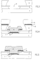
- FIG. 1 there are shown respectively conventional bipolar and Field Effect Transistor (FET) structures to illustrate contact hole structures.
- FET Field Effect Transistor
- a p-substrate 1 has formed therein n-, p+ and n+ regions by known techniques to produce a conventional NPN bipolar transistor structure.
- a insulation layer 2 and a passivation layer 3 are deposited through which holes 4 have been formed for purposes of making electrical contact with collector, base and emitter regions of the bipolar transistor structure.
- an FET structure has been formed in the substrate 1 wherein holes 4 in the insulation layer 2 and device passivation layer 3 have been formed for the purposes of making electrical contact with source and drain regions of the FET structure.
- holes 4 in the insulation layer 2 and device passivation layer 3 have been formed for the purposes of making electrical contact with source and drain regions of the FET structure.
- other examples will suggest themselves to those skilled in the art where electrical contact is required to be made to a semiconductor structure as, for example, Schottky barrier contacts.
- the present invention includes defining on a substrate, which has been processed to the point of being ready for the contact stud metallurgy such as shown in Figures 1 and 2, a lift-off stencil depicting the required stud pattern and aligned to the underlying semiconductor device contacts, and then Ti/Cr-CrO x /Al-Cu metallurgy is deposited by evaporation.
- Cr-CrO x as used herein represents chromium containing chromium oxide.
- the sacrificial aluminum alloy is then chemically etched out, leaving behind a pattern of holes in the insulating layer while the semiconductor surface is protected by the Ti/Cr-CrO x layers.
- a thin layer of Ti and tungsten is sputter deposited to act as adhesive and seed layers for the subsequent CVD tungsten deposition.
- the substrates are chemically-mechanically polished to remove excess metals. This leaves a pattern of tungsten studs self-aligned to the device contacts.
- the advantage of this process is that the semiconductor surface never comes in contact with any reactive chemicals, since it is protected by Ti and Cr-CrO x films. This also prevents any undesirable effects of the CVD tungsten, such as silicon encroachment. The added chrome further restricts any seepage of tungsten hexafluoride into the silicon surface. A reliable low ohmic contact is achieved, because the contact metallurgy of titanium is deposited at the very beginning.
- the substrate 1 represents a typical silicon wafer in which a plurality of semiconductor devices such as FET transistors, bipolar transistors, Schottky diodes, non-volatile devices, or a combination of them, are previously fabricated as represented in Figures 1 and 2.
- the device insulation and passivation layers 2 and 3 have holes 4, only one of which is illustrated for the sake of simplification, to make contact to semiconductor devices underneath.
- a lift-off stencil 5 is defined by a known lift-off technique.
- the stencil pattern corresponds to the set of contact holes 4 in a semiconductor substrate. If desired, this pattern may be personalized to have openings corresponding only to a select group of semiconductor contact holes 4.
- the total thickness of this composite metallurgy is adjusted by the aluminum alloy 8 to a total height of approximately 1.5X the predetermined height of the stud.
- the polymer of the lift-off stencil 5 is dissolved by standard methods as employed in various lift-off techniques, leaving an array of contact studs, represented by the single stud 8 shown in Figure 5.
- a layer of oxide, nitride or polyimide insulation 9 is then deposited to a thickness of 1.1X the predetermined stud height, as shown in Figure 6.
- the wafer is then planarized by any of the known processes, e.g., chemical-mechanical polishing, RIE or a combination of them, to the desired stud height, as shown in Figure 7.
- the aluminum alloy 8 is etched out by standard phosphoric-nitric acid etch, leaving intact the Ti/Cr-CrO x layers and an array of holes in the insulation layer 9, as shown in Figure 8. Then, a thin layer of titanium 10 and tungsten 11 is physically vapor deposited by thermal evaporation or sputtering in Figure 9. The titanium layer 10 is required here to make a low resistance contact with Cr-CrO x , and the tungsten layer 11 provides a seed layer for the next step of CVD tungsten deposition 12, shown in Figure 10.
- the CVD tungsten layer 12 is deposited with any of the known methods to a thickness of 0.9X the thickness of the insulator layer 10, and the excess tungsten is removed by chemical-mechanical polishing to produce the structure shown in Figure 11. This makes an array of planarized tungsten plugs 12 self-aligned and making low resistance ohmic contacts to semiconductor devices while protecting the semiconductor surface from harsh in-process chemical reactions causing silicon encroachment.
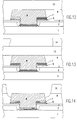
- a blanket layer of, for example, SiO2 insulator is deposited, and an interconnection line pattern is defined in a multi-layer structure of photoresist.
- the line pattern is etched into the insulator until the top surface of the studs are exposed.
- the sacrificial aluminum alloy is then chemically etched out, leaving cavities corresponding to contact stud pattern and self aligned to device contact holes.
- a thin layer of titanium and tungsten is sputter deposited to act as adhesive and seed layer followed by a thin layer of CVD tungsten deposition. Desired thickness of aluminum alloy is then deposited and the excess metallurgy is polished away by a chemical-mechanical polishing method. This method makes an integral structure of aluminum alloy contact stud and interconnection wire having tungsten lining on the sides and at base.
- the semiconductor surface protection and ohmic contact formation is still with Ti and Cr-CrO x layers.
- the process steps up to Figure 7 are exactly the same.
- a layer of insulation 13 e.g., oxide, nitride, polyimide or any combination of them, is deposited.
- the thickness of this insulation layer 13 is about 1.2X predetermined thickness of the interconnection lines.
- a pattern of interconnection lines is defined photolithographically on top of this insulation layer 13 using a multi-layer resist system 14, as shown in Figure 13.
- the insulation layer 13 is then reactively etched until the top surface of the underlying stud 8 is exposed. A slight over-etching is desirable to account for any variation in insulation thickness or its etch rate.
- the multi-layer resist 14 is stripped by oxygen plasma leaving the structure shown in Figure 14. Then, the exposed aluminum 8 is etched out by phosphoric-nitric acid in Figure 15.
- the structure shown in Figure 16 is built up beginning with a thin layer of titanium 14 and tungsten which is sputter deposited for a seed layer, followed by deposition of approximately 0.1 - 0.3 micron of CVD tungsten 15. A thin layer of titanium 16, and an alloy of Al-Cu 17 is next physical vapor deposited. The thickness of aluminum-copper alloy 17 is the sum of the interconnection line thickness and the stud thickness. The excess metallurgy is chemical-mechanical polished in Figure 17.
- Figure 17 shows the final configuration in accordance with the present invention comprising an integral contact stud and interconnection line of a conductor metal 17 lined with tungsten 15.
- Tungsten liner 15 acts as a barrier for alloying of the conductor metal (e.g., Al-Cu alloy here) with silicon of the substrate 1.
- Tungsten is deposited by CVD which conformally coats any fine crevice in the intricate contact hole geometry, and also provides a coaxial coating of the contact stud, thereby providing an efficient barrier.
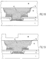
- an integral unit of tungsten lined interconnect wiring over, and together with coaxially tungsten-coated interlevel via studs making contact to lower level interconnections through an insulating layer is made by photolithographically defining the via stud pattern and reactive ion etching. This is shown in Figures 18 through 21.
- the interconnection lines on higher levels and the via stud connections to interconnection lines on lower levels are fabricated simultaneously as an integral structure. Starting with wafers or substrates processed to the step shown in Figure 17, an insulating layer 18 with thickness equivalent to about 1.2X the sum of predetermined thicknesses of second interconnection line metallurgy and via stud is deposited in Figure 18.
- a second level of interconnection line pattern is photolithographically defined on top of insulator 18, and the insulator is reactively etched to a depth approximately twenty percent thicker than the desired, predetermined interconnection metallurgy thickness, and the resist removed, as shown in Figure 19. Substrates are recoated with a multilayer resist to define the interlevel via stud pattern. The insulator 18 is further etched in Figure 20 until the top surface of the metallurgy 17 underneath is exposed, and the resist is then removed.
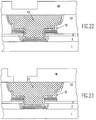
- the integral unit of tungsten lined interconnect wiring over, and together with coaxially tungsten-coated interlevel via studs making contact to lower level interconnections through an insulating layer is made as shown in Figures 22 and 23.
- the interconnection lines on higher levels and the via stud connections to interconnection lines on lower levels are fabricated simultaneously as an integral structure, but with a slightly different order in the processing steps.
- an insulating layer 18 with thickness equivalent to about 1.2X the sum of predetermined thicknesses of second interconnection line metallurgy and via stud is deposited as in Figure 18.
- the via stud pattern is first photolithographically defined on top of insulator 18, and the insulator is reactively etched and the resist removed, as shown in Figure 22. Substrates are recoated with a multi layer resist to define the interconnection line pattern.
- the insulator 18 is further etched in Figure 22 until the top surface of the metallurgy 17 underneath is exposed, and the resist is then removed. Further process steps are in accordance with process steps described above with respect to Figures 16 and 17. It should be apparent that given the guidance and the illustrations set forth herein, alternate embodiments of the processes and structures of the present invention may be suggested to a skilled artisan.
- titanium containing nitrogen, tantalum or tantalum containing nitrogen could be substituted for Cr-CrO x as the barrier layer.
- the insulator could include an organic or inorganic component or a combination thereof.
Landscapes
- Internal Circuitry In Semiconductor Integrated Circuit Devices (AREA)
- Electrodes Of Semiconductors (AREA)
Applications Claiming Priority (2)
| Application Number | Priority Date | Filing Date | Title |
|---|---|---|---|
| US08/005,961 US5434451A (en) | 1993-01-19 | 1993-01-19 | Tungsten liner process for simultaneous formation of integral contact studs and interconnect lines |
| US5961 | 2001-12-03 |
Publications (1)
| Publication Number | Publication Date |
|---|---|
| EP0609635A1 true EP0609635A1 (fr) | 1994-08-10 |
Family
ID=21718580
Family Applications (1)
| Application Number | Title | Priority Date | Filing Date |
|---|---|---|---|
| EP93480233A Withdrawn EP0609635A1 (fr) | 1993-01-19 | 1993-12-22 | Procédé comportant un enrobage de tungstène pour la formation simultanée de plots de contact et de lignes d'interconnexion ne formant qu'un |
Country Status (3)
| Country | Link |
|---|---|
| US (1) | US5434451A (fr) |
| EP (1) | EP0609635A1 (fr) |
| JP (1) | JP2576820B2 (fr) |
Cited By (1)
| Publication number | Priority date | Publication date | Assignee | Title |
|---|---|---|---|---|
| EP0890984A1 (fr) * | 1997-06-30 | 1999-01-13 | Siemens Aktiengesellschaft | Structure à double damasquinage et son procéde de fabrication |
Families Citing this family (23)
| Publication number | Priority date | Publication date | Assignee | Title |
|---|---|---|---|---|
| US5357397A (en) * | 1993-03-15 | 1994-10-18 | Hewlett-Packard Company | Electric field emitter device for electrostatic discharge protection of integrated circuits |
| US5448111A (en) * | 1993-09-20 | 1995-09-05 | Fujitsu Limited | Semiconductor device and method for fabricating the same |
| JP3469976B2 (ja) * | 1995-10-19 | 2003-11-25 | 三菱電機株式会社 | 多層配線の形成方法 |
| US5830774A (en) * | 1996-06-24 | 1998-11-03 | Motorola, Inc. | Method for forming a metal pattern on a substrate |
| US5795831A (en) * | 1996-10-16 | 1998-08-18 | Ulvac Technologies, Inc. | Cold processes for cleaning and stripping photoresist from surfaces of semiconductor wafers |
| US5963828A (en) * | 1996-12-23 | 1999-10-05 | Lsi Logic Corporation | Method for tungsten nucleation from WF6 using titanium as a reducing agent |
| US5981374A (en) * | 1997-04-29 | 1999-11-09 | International Business Machines Corporation | Sub-half-micron multi-level interconnection structure and process thereof |
| US5899738A (en) * | 1997-05-23 | 1999-05-04 | Taiwan Semiconductor Manufacturing Company, Ltd. | Method for making metal plugs in stacked vias for multilevel interconnections and contact openings while retaining the alignment marks without requiring extra masking steps |
| US6130161A (en) * | 1997-05-30 | 2000-10-10 | International Business Machines Corporation | Method of forming copper interconnections with enhanced electromigration resistance and reduced defect sensitivity |
| US6069068A (en) * | 1997-05-30 | 2000-05-30 | International Business Machines Corporation | Sub-quarter-micron copper interconnections with improved electromigration resistance and reduced defect sensitivity |
| US6133139A (en) * | 1997-10-08 | 2000-10-17 | International Business Machines Corporation | Self-aligned composite insulator with sub-half-micron multilevel high density electrical interconnections and process thereof |
| KR100526573B1 (ko) * | 1998-06-30 | 2006-01-12 | 주식회사 하이닉스반도체 | 반도체 소자의 금속 배선 형성 방법 |
| US6245668B1 (en) * | 1998-09-18 | 2001-06-12 | International Business Machines Corporation | Sputtered tungsten diffusion barrier for improved interconnect robustness |
| US6436814B1 (en) | 2000-11-21 | 2002-08-20 | International Business Machines Corporation | Interconnection structure and method for fabricating same |
| US6869853B1 (en) | 2002-12-18 | 2005-03-22 | Cypress Semiconductor Corporation | Fabrication of a bipolar transistor using a sacrificial emitter |
| US7273808B1 (en) | 2003-02-03 | 2007-09-25 | Novellus Systems, Inc. | Reactive barrier/seed preclean process for damascene process |
| US6825561B1 (en) | 2003-06-19 | 2004-11-30 | International Business Machines Corporation | Structure and method for eliminating time dependent dielectric breakdown failure of low-k material |
| US7435648B2 (en) * | 2006-07-26 | 2008-10-14 | Macronix International Co., Ltd. | Methods of trench and contact formation in memory cells |
| US7531443B2 (en) * | 2006-12-08 | 2009-05-12 | Micron Technology, Inc. | Method and system for fabricating semiconductor components with through interconnects and back side redistribution conductors |
| US8691687B2 (en) | 2010-01-07 | 2014-04-08 | International Business Machines Corporation | Superfilled metal contact vias for semiconductor devices |
| DE102013104953B4 (de) * | 2013-05-14 | 2023-03-02 | OSRAM Opto Semiconductors Gesellschaft mit beschränkter Haftung | Optoelektronisches Bauelement und Verfahren zu seiner Herstellung |
| US9773737B2 (en) | 2015-11-23 | 2017-09-26 | International Business Machines Corporation | Advanced metallization for damage repair |
| US9601432B1 (en) | 2015-11-23 | 2017-03-21 | International Business Machines Corporation | Advanced metallization for damage repair |
Citations (5)
| Publication number | Priority date | Publication date | Assignee | Title |
|---|---|---|---|---|
| US4214256A (en) * | 1978-09-08 | 1980-07-22 | International Business Machines Corporation | Tantalum semiconductor contacts and method for fabricating same |
| DE3021206A1 (de) * | 1979-06-06 | 1980-12-11 | Tokyo Shibaura Electric Co | Verfahren zur herstellung einer halbleitervorrichtung |
| EP0425787A2 (fr) * | 1989-10-31 | 1991-05-08 | International Business Machines Corporation | Procédé de fabrication de lignes de métaux à haute densité auto-alignée aux fenêtres de contact |
| EP0453644A2 (fr) * | 1990-04-27 | 1991-10-30 | Siemens Aktiengesellschaft | Procédé pour la fabrication d'un trou dans une structure semi-conductrice en couches et son utilisation pour la fabrication des trous de contact |
| EP0506129A1 (fr) * | 1991-03-29 | 1992-09-30 | Applied Materials, Inc. | Procédé de formation d'un contact électrique à travers une couche isolante sur une pastille semi-conductrice |
Family Cites Families (11)
| Publication number | Priority date | Publication date | Assignee | Title |
|---|---|---|---|---|
| US4029562A (en) * | 1976-04-29 | 1977-06-14 | Ibm Corporation | Forming feedthrough connections for multi-level interconnections metallurgy systems |
| US4410622A (en) * | 1978-12-29 | 1983-10-18 | International Business Machines Corporation | Forming interconnections for multilevel interconnection metallurgy systems |
| US4519872A (en) * | 1984-06-11 | 1985-05-28 | International Business Machines Corporation | Use of depolymerizable polymers in the fabrication of lift-off structure for multilevel metal processes |
| JPS62274715A (ja) * | 1986-05-23 | 1987-11-28 | Nec Corp | 半導体装置の製造方法 |
| US4884123A (en) * | 1987-02-19 | 1989-11-28 | Advanced Micro Devices, Inc. | Contact plug and interconnect employing a barrier lining and a backfilled conductor material |
| US5008216A (en) * | 1988-10-03 | 1991-04-16 | International Business Machines Corporation | Process for improved contact stud structure for semiconductor devices |
| JPH04199628A (ja) * | 1990-11-29 | 1992-07-20 | Seiko Epson Corp | 半導体装置の製造方法 |
| JP2660359B2 (ja) * | 1991-01-30 | 1997-10-08 | 三菱電機株式会社 | 半導体装置 |
| JPH0567615A (ja) * | 1991-04-03 | 1993-03-19 | Sharp Corp | 半導体装置及びその製造方法 |
| JPH05234935A (ja) * | 1992-02-20 | 1993-09-10 | Matsushita Electron Corp | 半導体装置及びその製造方法 |
| JPH05283536A (ja) * | 1992-03-31 | 1993-10-29 | Nec Corp | 半導体装置のコンタクトホール埋め込み方法 |
-
1993
- 1993-01-19 US US08/005,961 patent/US5434451A/en not_active Expired - Lifetime
- 1993-12-22 EP EP93480233A patent/EP0609635A1/fr not_active Withdrawn
- 1993-12-28 JP JP5334516A patent/JP2576820B2/ja not_active Expired - Lifetime
Patent Citations (5)
| Publication number | Priority date | Publication date | Assignee | Title |
|---|---|---|---|---|
| US4214256A (en) * | 1978-09-08 | 1980-07-22 | International Business Machines Corporation | Tantalum semiconductor contacts and method for fabricating same |
| DE3021206A1 (de) * | 1979-06-06 | 1980-12-11 | Tokyo Shibaura Electric Co | Verfahren zur herstellung einer halbleitervorrichtung |
| EP0425787A2 (fr) * | 1989-10-31 | 1991-05-08 | International Business Machines Corporation | Procédé de fabrication de lignes de métaux à haute densité auto-alignée aux fenêtres de contact |
| EP0453644A2 (fr) * | 1990-04-27 | 1991-10-30 | Siemens Aktiengesellschaft | Procédé pour la fabrication d'un trou dans une structure semi-conductrice en couches et son utilisation pour la fabrication des trous de contact |
| EP0506129A1 (fr) * | 1991-03-29 | 1992-09-30 | Applied Materials, Inc. | Procédé de formation d'un contact électrique à travers une couche isolante sur une pastille semi-conductrice |
Cited By (1)
| Publication number | Priority date | Publication date | Assignee | Title |
|---|---|---|---|---|
| EP0890984A1 (fr) * | 1997-06-30 | 1999-01-13 | Siemens Aktiengesellschaft | Structure à double damasquinage et son procéde de fabrication |
Also Published As
| Publication number | Publication date |
|---|---|
| JPH06244135A (ja) | 1994-09-02 |
| JP2576820B2 (ja) | 1997-01-29 |
| US5434451A (en) | 1995-07-18 |
Similar Documents
| Publication | Publication Date | Title |
|---|---|---|
| US5434451A (en) | Tungsten liner process for simultaneous formation of integral contact studs and interconnect lines | |
| US6445073B1 (en) | Damascene metallization process and structure | |
| EP0279588B1 (fr) | Contact dans une perforation dans un semi-conducteur et procédé pour sa fabrication | |
| US6211049B1 (en) | Forming submicron integrated-circuit wiring from gold, silver, copper, and other metals | |
| US6426289B1 (en) | Method of fabricating a barrier layer associated with a conductor layer in damascene structures | |
| US6133139A (en) | Self-aligned composite insulator with sub-half-micron multilevel high density electrical interconnections and process thereof | |
| US8461692B2 (en) | Semiconductor device structures including damascene trenches with conductive structures and related method | |
| EP0761014B1 (fr) | Procede simplifie de double damasquinage servant a effectuer une metallisation a des niveaux multiples et a realiser une structure d'interconnexion | |
| US6492722B1 (en) | Metallized interconnection structure | |
| US4960732A (en) | Contact plug and interconnect employing a barrier lining and a backfilled conductor material | |
| US5981374A (en) | Sub-half-micron multi-level interconnection structure and process thereof | |
| US5227335A (en) | Tungsten metallization | |
| US6653737B2 (en) | Interconnection structure and method for fabricating same | |
| US6051880A (en) | Base layer structure covering a hole of decreasing diameter in an insulation layer in a semiconductor device | |
| US6180509B1 (en) | Method for forming planarized multilevel metallization in an integrated circuit | |
| US6001734A (en) | Formation method of contact/ through hole | |
| US20040171256A1 (en) | Mask layer and interconnect structure for dual damascene semiconductor manufacturing | |
| KR100554210B1 (ko) | 자기 정렬 상호접속 비아를 이용하는 이중 다마신법 | |
| KR0178406B1 (ko) | 반도체 장치 제조방법 | |
| JPS63244858A (ja) | 金属配線の形成方法 | |
| JP2618460B2 (ja) | 電気接続体の形成方法 | |
| EP0507881A1 (fr) | Structure d'interconnexion pour dispositif semiconducteur utilisant un isolateur en polyimide | |
| EP1317772B1 (fr) | Structure d'interconnexion semi-conductrice et son procede de fabrication | |
| US6297144B1 (en) | Damascene local interconnect process | |
| KR100396687B1 (ko) | 반도채장치의금속배선형성방법 |
Legal Events
| Date | Code | Title | Description |
|---|---|---|---|
| PUAI | Public reference made under article 153(3) epc to a published international application that has entered the european phase |
Free format text: ORIGINAL CODE: 0009012 |
|
| AK | Designated contracting states |
Kind code of ref document: A1 Designated state(s): DE FR GB |
|
| 17P | Request for examination filed |
Effective date: 19941125 |
|
| 17Q | First examination report despatched |
Effective date: 19960430 |
|
| STAA | Information on the status of an ep patent application or granted ep patent |
Free format text: STATUS: THE APPLICATION IS DEEMED TO BE WITHDRAWN |
|
| 18D | Application deemed to be withdrawn |
Effective date: 19980701 |