EP0611203A1 - Einen thermischen Isolator aus expandiertem Polymer enthaltender thermischer Detector - Google Patents
Einen thermischen Isolator aus expandiertem Polymer enthaltender thermischer Detector Download PDFInfo
- Publication number
- EP0611203A1 EP0611203A1 EP94400267A EP94400267A EP0611203A1 EP 0611203 A1 EP0611203 A1 EP 0611203A1 EP 94400267 A EP94400267 A EP 94400267A EP 94400267 A EP94400267 A EP 94400267A EP 0611203 A1 EP0611203 A1 EP 0611203A1
- Authority
- EP
- European Patent Office
- Prior art keywords
- layer
- polymer
- detector according
- thermal detector
- thermal
- Prior art date
- Legal status (The legal status is an assumption and is not a legal conclusion. Google has not performed a legal analysis and makes no representation as to the accuracy of the status listed.)
- Granted
Links
- 229920000642 polymer Polymers 0.000 title claims abstract description 53
- 239000012212 insulator Substances 0.000 title description 2
- 239000000463 material Substances 0.000 claims abstract description 38
- 239000000758 substrate Substances 0.000 claims abstract description 29
- 230000005855 radiation Effects 0.000 claims abstract description 7
- 239000002904 solvent Substances 0.000 claims description 28
- 239000004642 Polyimide Substances 0.000 claims description 18
- 238000000034 method Methods 0.000 claims description 18
- 229920001721 polyimide Polymers 0.000 claims description 18
- 238000004519 manufacturing process Methods 0.000 claims description 17
- 238000009413 insulation Methods 0.000 claims description 9
- 230000008569 process Effects 0.000 claims description 8
- 238000010438 heat treatment Methods 0.000 claims description 7
- 239000002243 precursor Substances 0.000 claims description 7
- 229910052724 xenon Inorganic materials 0.000 claims description 7
- FHNFHKCVQCLJFQ-UHFFFAOYSA-N xenon atom Chemical compound [Xe] FHNFHKCVQCLJFQ-UHFFFAOYSA-N 0.000 claims description 7
- OKKJLVBELUTLKV-UHFFFAOYSA-N Methanol Chemical group OC OKKJLVBELUTLKV-UHFFFAOYSA-N 0.000 claims description 6
- 239000000126 substance Substances 0.000 claims description 6
- 239000011159 matrix material Substances 0.000 claims description 5
- 239000002033 PVDF binder Substances 0.000 claims description 4
- 238000005530 etching Methods 0.000 claims description 4
- 238000001465 metallisation Methods 0.000 claims description 4
- 229920002981 polyvinylidene fluoride Polymers 0.000 claims description 4
- SECXISVLQFMRJM-UHFFFAOYSA-N N-Methylpyrrolidone Chemical compound CN1CCCC1=O SECXISVLQFMRJM-UHFFFAOYSA-N 0.000 claims description 3
- 239000012298 atmosphere Substances 0.000 claims description 3
- 239000000919 ceramic Substances 0.000 claims description 3
- 230000008030 elimination Effects 0.000 claims description 3
- 238000003379 elimination reaction Methods 0.000 claims description 3
- 229920005575 poly(amic acid) Polymers 0.000 claims description 3
- 230000004044 response Effects 0.000 claims description 3
- 238000007654 immersion Methods 0.000 claims 1
- 238000000206 photolithography Methods 0.000 claims 1
- -1 polyvinylene fluoride-trifluoroethylene Polymers 0.000 claims 1
- 239000010409 thin film Substances 0.000 abstract description 2
- 239000000243 solution Substances 0.000 description 13
- ZMXDDKWLCZADIW-UHFFFAOYSA-N N,N-Dimethylformamide Chemical compound CN(C)C=O ZMXDDKWLCZADIW-UHFFFAOYSA-N 0.000 description 6
- 239000010408 film Substances 0.000 description 6
- 238000005119 centrifugation Methods 0.000 description 5
- 238000001035 drying Methods 0.000 description 5
- 229910052782 aluminium Inorganic materials 0.000 description 4
- XAGFODPZIPBFFR-UHFFFAOYSA-N aluminium Chemical compound [Al] XAGFODPZIPBFFR-UHFFFAOYSA-N 0.000 description 4
- 238000004377 microelectronic Methods 0.000 description 4
- 239000011148 porous material Substances 0.000 description 4
- XUIMIQQOPSSXEZ-UHFFFAOYSA-N Silicon Chemical compound [Si] XUIMIQQOPSSXEZ-UHFFFAOYSA-N 0.000 description 3
- 229910052710 silicon Inorganic materials 0.000 description 3
- 239000010703 silicon Substances 0.000 description 3
- 230000004888 barrier function Effects 0.000 description 2
- 230000008901 benefit Effects 0.000 description 2
- 238000005345 coagulation Methods 0.000 description 2
- 230000015271 coagulation Effects 0.000 description 2
- 238000009792 diffusion process Methods 0.000 description 2
- 238000001704 evaporation Methods 0.000 description 2
- 230000008020 evaporation Effects 0.000 description 2
- 238000005191 phase separation Methods 0.000 description 2
- 238000001020 plasma etching Methods 0.000 description 2
- 239000004065 semiconductor Substances 0.000 description 2
- VYZAMTAEIAYCRO-UHFFFAOYSA-N Chromium Chemical compound [Cr] VYZAMTAEIAYCRO-UHFFFAOYSA-N 0.000 description 1
- RTAQQCXQSZGOHL-UHFFFAOYSA-N Titanium Chemical compound [Ti] RTAQQCXQSZGOHL-UHFFFAOYSA-N 0.000 description 1
- 239000002250 absorbent Substances 0.000 description 1
- 230000002745 absorbent Effects 0.000 description 1
- 239000002318 adhesion promoter Substances 0.000 description 1
- 238000000137 annealing Methods 0.000 description 1
- 210000003850 cellular structure Anatomy 0.000 description 1
- 239000013522 chelant Substances 0.000 description 1
- 229910052804 chromium Inorganic materials 0.000 description 1
- 239000011651 chromium Substances 0.000 description 1
- 238000000576 coating method Methods 0.000 description 1
- 239000004020 conductor Substances 0.000 description 1
- 238000001816 cooling Methods 0.000 description 1
- 229920001577 copolymer Polymers 0.000 description 1
- 238000000151 deposition Methods 0.000 description 1
- 238000010790 dilution Methods 0.000 description 1
- 239000012895 dilution Substances 0.000 description 1
- 230000005684 electric field Effects 0.000 description 1
- 239000003822 epoxy resin Substances 0.000 description 1
- 239000007789 gas Substances 0.000 description 1
- 230000006872 improvement Effects 0.000 description 1
- 238000003331 infrared imaging Methods 0.000 description 1
- 239000007788 liquid Substances 0.000 description 1
- 229910052751 metal Inorganic materials 0.000 description 1
- 239000002184 metal Substances 0.000 description 1
- 239000012299 nitrogen atmosphere Substances 0.000 description 1
- 238000000614 phase inversion technique Methods 0.000 description 1
- 229920000647 polyepoxide Polymers 0.000 description 1
- 239000002861 polymer material Substances 0.000 description 1
- 229920000131 polyvinylidene Polymers 0.000 description 1
- HNJBEVLQSNELDL-UHFFFAOYSA-N pyrrolidin-2-one Chemical compound O=C1CCCN1 HNJBEVLQSNELDL-UHFFFAOYSA-N 0.000 description 1
- 230000000284 resting effect Effects 0.000 description 1
- 238000007789 sealing Methods 0.000 description 1
- 230000035945 sensitivity Effects 0.000 description 1
- FZHAPNGMFPVSLP-UHFFFAOYSA-N silanamine Chemical class [SiH3]N FZHAPNGMFPVSLP-UHFFFAOYSA-N 0.000 description 1
- 239000007787 solid Substances 0.000 description 1
- 239000007921 spray Substances 0.000 description 1
- 238000003756 stirring Methods 0.000 description 1
- 239000010936 titanium Substances 0.000 description 1
- 229910052719 titanium Inorganic materials 0.000 description 1
- 238000007738 vacuum evaporation Methods 0.000 description 1
Images

Classifications
-
- H—ELECTRICITY
- H10—SEMICONDUCTOR DEVICES; ELECTRIC SOLID-STATE DEVICES NOT OTHERWISE PROVIDED FOR
- H10N—ELECTRIC SOLID-STATE DEVICES NOT OTHERWISE PROVIDED FOR
- H10N15/00—Thermoelectric devices without a junction of dissimilar materials; Thermomagnetic devices, e.g. using the Nernst-Ettingshausen effect
- H10N15/10—Thermoelectric devices using thermal change of the dielectric constant, e.g. working above and below the Curie point
Definitions
- the present invention relates to the general field of infrared detectors operating at ambient temperature and in particular detectors comprising a pyroelectric material.
- thermal detectors making it possible in particular to produce infrared imagers, these detectors operating at room temperature without a cooling system.
- the sensitive material included in the detector is heated by infrared radiation. Under the rise in temperature, charges may appear (pyroelectric detector), variations in dielectric constant (dielectric bolometer), variations in resistance (resistive bolometer) ...
- the major problem of these detectors is to confine the heat to within the sensitive material, avoiding as much as possible the losses by diffusion within the substrate comprising the circuits for reading the response of the sensitive material.
- Another solution proposes using pyroelectric polymers of low conductivity as sensitive layers which can accommodate less sophisticated thermal insulation (FR 89 08799). It is notably proposed to use for example a conventional dielectric layer of polyimide type, between the silicon reading circuit and the pyroelectric polymer. We thus manage to reduce the losses by diffusion at the sensitive layer, with a collective manufacturing method of microelectronics type but the performances and the sensitivities of these detectors still require to turn to other solutions to further improve the insulation. thermal.
- the subject of the invention is a thermal detector comprising a layer of material sensitive to infrared radiation comprised between electrodes, a substrate comprising a circuit for reading the response of the sensitive material, characterized in that the detector comprises between the layer of sensitive material and the substrate, a layer of thermostable polymer of microporous structure having a reduced thermal conductivity.
- thermostable polymer can advantageously be of the polyimide type.
- the sensitive material can advantageously be ferroelectric, it can be a polymer or a ceramic.
- the pyroelectric material can advantageously be comprised between a continuous electrode and a set of conductive pads arranged matrix on the layer of polymer of microporous structure, so as to define image or pixel elements, the layer of this polymer further comprising vias. conductors connecting the conductive pads to the reading circuit integrated into the substrate.
- the sensitive material can also be a thermoresistive material such as VO2 oxide.
- the demixing step can advantageously be obtained by immersing the layer C1 on the substrate in a product B which is non-solvent for the polymer and miscible with solvent A.
- the removal of the solvent can then be carried out simultaneously with that of product B by treatment. thermal.
- the polymer dissolved in solvent A can advantageously be a precursor of the polyimide.
- the solvent removal step A is in this case, followed by a high temperature heat treatment so as to transform the precursor into polyimide.
- the demixing step can also be obtained by heat treatment at a temperature T1 such that there is appearance of phase separation at this temperature the solvent of the polymer is then evaporated under vacuum at this temperature.
- the sensitive material of layer C2 can be of the pyroelectric polymer type which can easily be deposited in a thin layer. It may especially be a polymer of polyvinylidene fluoride type or of polyvinylidene fluoride-trifluoroethylene type.
- the sensitive material of layer C2 can also be a ferroelectric ceramic that can be deposited in a thin layer, in particular by sol-gel techniques.
- the advantage of these production methods is that they only use thin film techniques which make it possible to obtain small infrared detectors.
- an improvement of the invention consists in ensuring that the micropores of the polymer layer are filled not with air but with a substance having better thermal insulation properties than air, for result in an even more thermally insulating layer.
- Xenon is particularly suitable: it can easily be incorporated into the layer and remain trapped there.
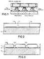
- FIG. 1 represents an infrared detector based on pyroelectric material according to the Hugues Patent Application cited above.
- This detector comprises elements made of pyroelectric material, one per pixel, between a continuous electrode and elementary electrodes. Conductive pads electrically connect the elementary electrodes to the inputs of processing circuits developed on a semiconductor substrate.
- This type of hybrid structure remains much more complex than structures achievable only by collective techniques in thin layers such as those used in microelectronics. This is why the invention proposes a thermal detector in which the use of a thermostable material which can be deposited in a thin layer and of significantly reduced thermal conductivity makes it possible to develop a structure in which a thin layer of sensitive material is produced on a substrate. comprising a reading circuit, said layer being thermally decoupled from the substrate by a layer of thermostable material.
- the substrate used can advantageously be a semiconductor substrate of the silicon type comprising reading circuits.
- the substrate may include processing circuits and a 2-dimensional matrix of read switches.
- the thermal detector according to the invention comprises a layer constituting the thermal barrier, this layer being provided with conductive vias, making it possible to ensure the electrical contacts between the elements of the reading circuit and the lower electrodes with which the layer of sensitive material is provided. we want to record the physical variations during a temperature variation.
- the layer constituting the thermal barrier is a layer of thermostable polymer of the polyimide type.
- This layer can be obtained from a solution by a conventional coating process (spray, centrifugation, pouring ). It is advantageous to use a polymer precursor solution of the polyimide type (the polyimide being hardly soluble) conventionally used for the production of insulating layers in microelectronics.
- phase separation or phase inversion Before drying of this solution, the technique known as phase separation or phase inversion is applied, the aim of which is to transform in this layer, the solution, initially homogeneous, into a two-phase system making it possible to obtain a phase rich in polymer which will constitute after drying a solid network, and, a phase poor in polymer which will constitute a network of pores.
- This complex structure thus leads to the development of a polymer with a microporous structure, the thermal conductivity of which is significantly lowered, after evaporation of a solvent from the initial solution containing the thermostable polymer.
- phase inversion operation can be obtained by coagulation of the solution by immersing it in a bath of non-solvent for the polymer, but miscible with the solvent of said solution.
- an "expanded" polymer After removing the solvent and the non-solvent by drying and after heat treatment in order to stabilize the structure, in particular in the case of a polyimide precursor which it is desired to imidize, an "expanded" polymer is obtained whose microporous structure gives it a low density and thus reduced thermal conductivity.
- the layer thus obtained can typically have a thickness of between 1 micron and a few hundred microns.
- a C0 bonding layer or an adhesion promoter In the particular case, it may be polyimides, aminosilanes or aluminum chelate. It is also possible to produce, before depositing the layer of polymer which will be made porous, a thin layer of polymer (preferably the same) dried but not fully annealed in order to be able to ally with this layer during the final heat treatment. .
- a surface area C ′ 1a by subjecting the upper face of the deposit to brief drying before the phase inversion step.
- This summary drying is carried out by carrying out a temperature gradient within the layer.
- the etching of the connection vias can be carried out in a similar manner to that of the conventional polymers used in microelectronics. It can be plasma etching or photoablation by Excimer laser.
- the thermally insulating layer makes it possible to etch the latter at a speed greater than that of the same unexpanded polymer, which thus makes it possible to produce layers of greater thickness while retaining the same etching process.
- a first thin layer of polyamic acid solution is applied (for example the material referenced PIQ 13 HITACHI) precursor of polyimide dissolved in solvent A or N Methyl-Pyrrolidone, by centrifugation at the spinner.
- the dilution of the solution and the centrifugation speed are adjusted in order to obtain a final thickness of the order of 0.5 ⁇ m.
- This layer is then dried for 10 minutes at 200 ° C and constitutes a bonding layer C0 on the substrate (S). On this layer, the layer intended to be expanded is deposited. The solution is then more concentrated and the centrifugation speed is reduced to obtain a greater thickness (of the order of 10 ⁇ m).
- the solvent A is briefly evaporated on the surface of the deposit in a ventilated oven at 80 ° C for 2 minutes.
- phase inversion is then carried out by immersing the substrate covered with the bonding layer and the partially densified layer, in a large quantity of non-solvent B with stirring.
- This non-solvent can be methanol or a chlorinated solvent, miscible with N-Methyl Pyrrolidone. After a few minutes, the originally transparent layer becomes completely diffusing when the medium is separated into two phases.
- the layer is dried under vacuum and then heat treated at 300 ° C to transform the polyamic acid into polyimide. We then obtain the layer C′1 and a structure illustrated in FIG. 2.
- connection vias (VC) are then etched in this layer of expanded polymer to access the reading elements as illustrated in FIG. 3, by reactive ion etching.
- the layer of sensitive material is then deposited, for example a layer of pyroelectric polymer of reduced thermal conductivity: for example, a PVDF - TrFE 75- copolymer 25 (75% by mole of PVDF for 25% by mole of TrFE) in dimethylformamide (DMF).
- a PVDF - TrFE 75- copolymer 25 75% by mole of PVDF for 25% by mole of TrFE
- DMF dimethylformamide
- a continuous electrode (E) is then deposited to form a counter-electrode, for example in the form of an aluminum layer 1000 Angstroms thick, by vacuum evaporation.
- a last layer of infrared absorbent (A) can finally be deposited on the continuous electrode (E); it may especially be aluminum black obtained by evaporation of aluminum under a nitrogen atmosphere according to a known technique.
- the continuous electrode (E) can also ensure the function of the layer (A) by being made of metal of titanium or chromium type.
- the thermal detector After having polarized the pyroelectric polymer material, typically with a continuous electric field close to 100 V / ⁇ m, the thermal detector thus obtained is able to function.
- a pyroelectric current normalized to 1 is measured under the influence of a CO2 laser radiation at 10.6 ⁇ m at a frequency of 50 Hz.
- the micropores of the layer are filled not with air but with a substance which has a better thermal insulation coefficient than that of air.
- the substance can be liquid or gaseous.
- the pores can be filled with xenon which is better thermal insulator than air. Xenon is placed in the pores for example if the solvent elimination annealing is carried out in a xenon atmosphere instead of being carried out in an ambient atmosphere. After the microporous layer has formed, the xenon remains trapped in the pores.
Landscapes
- Photometry And Measurement Of Optical Pulse Characteristics (AREA)
- Radiation Pyrometers (AREA)
Applications Claiming Priority (2)
| Application Number | Priority Date | Filing Date | Title |
|---|---|---|---|
| FR9301609 | 1993-02-12 | ||
| FR9301609A FR2701602B1 (fr) | 1993-02-12 | 1993-02-12 | Détecteur thermique comprenant un isolant thermique en polymère expansé. |
Publications (2)
| Publication Number | Publication Date |
|---|---|
| EP0611203A1 true EP0611203A1 (de) | 1994-08-17 |
| EP0611203B1 EP0611203B1 (de) | 1998-05-06 |
Family
ID=9444010
Family Applications (1)
| Application Number | Title | Priority Date | Filing Date |
|---|---|---|---|
| EP94400267A Expired - Lifetime EP0611203B1 (de) | 1993-02-12 | 1994-02-08 | Verfahren zur Herstellung eines thermischen Detektors |
Country Status (6)
| Country | Link |
|---|---|
| US (2) | US5418365A (de) |
| EP (1) | EP0611203B1 (de) |
| JP (1) | JPH06300622A (de) |
| CA (1) | CA2115400C (de) |
| DE (1) | DE69409990T2 (de) |
| FR (1) | FR2701602B1 (de) |
Cited By (1)
| Publication number | Priority date | Publication date | Assignee | Title |
|---|---|---|---|---|
| CN112557158A (zh) * | 2021-02-28 | 2021-03-26 | 中国工程物理研究院核物理与化学研究所 | 一种用于空气样品中氙的分离纯化收集装置 |
Families Citing this family (15)
| Publication number | Priority date | Publication date | Assignee | Title |
|---|---|---|---|---|
| FR2724750B1 (fr) * | 1994-09-16 | 1996-12-06 | Thomson Csf | Carte electronique avec voyant de bon fonctionnement |
| FR2770932B1 (fr) | 1997-11-07 | 2001-11-16 | Thomson Csf | Procede de fabrication d'une sonde acoustique |
| FR2779575B1 (fr) | 1998-06-05 | 2003-05-30 | Thomson Csf | Sonde acoustique multielements comprenant un film composite conducteur et procede de fabrication |
| ATE323132T1 (de) | 1998-11-24 | 2006-04-15 | Dow Global Technologies Inc | Eine zusammensetzung enthaltend einen vernetzbaren matrixpercursor und eine porenstruktur bildendes material und eine daraus hergestellte poröse matrix |
| FR2789822B1 (fr) | 1999-02-12 | 2001-06-08 | Thomson Csf | Dispositif a ondes de surface connecte a une embase avec un adhesif conducteur |
| FR2799883B1 (fr) | 1999-10-15 | 2003-05-30 | Thomson Csf | Procede d'encapsulation de composants electroniques |
| US20020095307A1 (en) * | 2000-10-27 | 2002-07-18 | Manugistics, Inc. | System and method for inventory and capacity availability management |
| US7668761B2 (en) * | 2000-10-27 | 2010-02-23 | Jda Software Group | System and method for ensuring order fulfillment |
| FR2819143B1 (fr) * | 2000-12-28 | 2003-03-07 | Thomson Csf | Procede de realisation de plots de connexion sur un circuit imprime |
| US7579070B2 (en) * | 2005-08-30 | 2009-08-25 | Intel Corporation | Multiple layer deposition for improving adhesion |
| US7408158B2 (en) * | 2006-05-26 | 2008-08-05 | Mengel Arthur H | Gas sensor apparatus |
| US9219264B2 (en) * | 2012-07-10 | 2015-12-22 | Samsung Sdi Co., Ltd. | Separator for rechargeable lithium battery and rechargeable lithium battery including the same |
| WO2014047523A2 (en) * | 2012-09-21 | 2014-03-27 | California Institute Of Technology | Methods and devices for sample lysis |
| FR3074574B1 (fr) * | 2017-12-04 | 2020-01-03 | Commissariat A L'energie Atomique Et Aux Energies Alternatives | Capteur de motif thermique a capacite pyroelectrique |
| CN115241364A (zh) * | 2022-07-25 | 2022-10-25 | 江苏大学 | 一种钽酸锂热释电红外探测器及其制造方法 |
Citations (4)
| Publication number | Priority date | Publication date | Assignee | Title |
|---|---|---|---|---|
| JPS58154151A (ja) * | 1982-03-09 | 1983-09-13 | Matsushita Electric Ind Co Ltd | タ−ゲツト構体 |
| EP0284131A1 (de) * | 1987-03-13 | 1988-09-28 | Philips Electronics Uk Limited | Thermischer Bildsensor und dessen Herstellungsmethode |
| EP0413461A1 (de) * | 1989-07-31 | 1991-02-20 | Texas Instruments Incorporated | Polyimid-Mesa zur thermischen Isolierung von thermischen Bildaufnahmegeräten |
| EP0435397A1 (de) * | 1989-12-29 | 1991-07-03 | Laboratoires D'electronique Philips | Pyroelektrisches Sensorelement und Vorrichtungen zur Erfassung thermischer Erscheinungen |
Family Cites Families (7)
| Publication number | Priority date | Publication date | Assignee | Title |
|---|---|---|---|---|
| FR2581482B1 (fr) * | 1985-05-03 | 1987-07-10 | Labo Electronique Physique | Photodiode pin a faible courant de fuite |
| EP0228712B1 (de) * | 1986-01-06 | 1995-08-09 | Sel Semiconductor Energy Laboratory Co., Ltd. | Photoelektrische Umwandlungsvorrichtung mit hoher Ansprechgeschwindigkeit und Herstellungsverfahren |
| US4740700A (en) * | 1986-09-02 | 1988-04-26 | Hughes Aircraft Company | Thermally insulative and electrically conductive interconnect and process for making same |
| FR2649247B1 (fr) * | 1989-06-30 | 1991-09-13 | Thomson Csf | Detecteur infrarouge a base de materiau pyroelectrique |
| US5034608A (en) * | 1989-09-08 | 1991-07-23 | Massachusetts Institute Of Technology | Infrared sensor operable without cooling |
| FR2670325B1 (fr) * | 1990-12-11 | 1993-01-22 | Thomson Composants Militaires | Detecteur infrarouge monolithique a materiau pyroelectrique. |
| GB2263084B (en) * | 1991-12-20 | 1995-07-05 | Micropore International Ltd | Shaping panels of microporous thermal insulation |
-
1993
- 1993-02-12 FR FR9301609A patent/FR2701602B1/fr not_active Expired - Fee Related
-
1994
- 1994-02-08 EP EP94400267A patent/EP0611203B1/de not_active Expired - Lifetime
- 1994-02-08 DE DE69409990T patent/DE69409990T2/de not_active Expired - Lifetime
- 1994-02-09 US US08/193,741 patent/US5418365A/en not_active Expired - Lifetime
- 1994-02-10 CA CA002115400A patent/CA2115400C/fr not_active Expired - Fee Related
- 1994-02-14 JP JP6039141A patent/JPH06300622A/ja active Pending
-
1995
- 1995-02-15 US US08/389,143 patent/US5618737A/en not_active Expired - Lifetime
Patent Citations (4)
| Publication number | Priority date | Publication date | Assignee | Title |
|---|---|---|---|---|
| JPS58154151A (ja) * | 1982-03-09 | 1983-09-13 | Matsushita Electric Ind Co Ltd | タ−ゲツト構体 |
| EP0284131A1 (de) * | 1987-03-13 | 1988-09-28 | Philips Electronics Uk Limited | Thermischer Bildsensor und dessen Herstellungsmethode |
| EP0413461A1 (de) * | 1989-07-31 | 1991-02-20 | Texas Instruments Incorporated | Polyimid-Mesa zur thermischen Isolierung von thermischen Bildaufnahmegeräten |
| EP0435397A1 (de) * | 1989-12-29 | 1991-07-03 | Laboratoires D'electronique Philips | Pyroelektrisches Sensorelement und Vorrichtungen zur Erfassung thermischer Erscheinungen |
Non-Patent Citations (1)
| Title |
|---|
| PATENT ABSTRACTS OF JAPAN vol. 7, no. 272 (E - 214) 13 December 1983 (1983-12-13) * |
Cited By (1)
| Publication number | Priority date | Publication date | Assignee | Title |
|---|---|---|---|---|
| CN112557158A (zh) * | 2021-02-28 | 2021-03-26 | 中国工程物理研究院核物理与化学研究所 | 一种用于空气样品中氙的分离纯化收集装置 |
Also Published As
| Publication number | Publication date |
|---|---|
| CA2115400C (fr) | 2009-04-21 |
| US5418365A (en) | 1995-05-23 |
| US5618737A (en) | 1997-04-08 |
| FR2701602A1 (fr) | 1994-08-19 |
| CA2115400A1 (fr) | 1994-08-13 |
| JPH06300622A (ja) | 1994-10-28 |
| FR2701602B1 (fr) | 1995-03-31 |
| DE69409990T2 (de) | 1998-09-03 |
| EP0611203B1 (de) | 1998-05-06 |
| DE69409990D1 (de) | 1998-06-10 |
Similar Documents
| Publication | Publication Date | Title |
|---|---|---|
| EP0611203B1 (de) | Verfahren zur Herstellung eines thermischen Detektors | |
| EP1636130B1 (de) | Integrierte schaltung auf hochleistungschip | |
| EP1058837B1 (de) | Kapazitive sensoren zur messung der feuchtigkeit und deren verfahren zur herstellung | |
| CA1195011A (fr) | Procede de realisation d'un hygrometre capacitif a dielectrique mince et hygrometre obtenu par ce procede | |
| FR2480673A1 (fr) | Couches portantes, et procede pour leur fabrication, en particulier pour des detecteurs sur des moteurs a combustion interne | |
| KR100530440B1 (ko) | 열 검출기 어레이 | |
| FR2689314A1 (fr) | Circuit intégré comprenant un film isolant intercouche et procédé pour sa production. | |
| FR2697675A1 (fr) | Procédé de fabrication de transducteurs capacitifs intégrés. | |
| FR2815953A1 (fr) | Composant micromecanique et procede de fabrication d'un tel composant | |
| FR2554237A1 (fr) | Capteur d'humidite et son procede de fabrication | |
| FR3045148A1 (fr) | Dispositif de detection a membranes bolometriques suspendues a fort rendement d'absorption et rapport signal sur bruit | |
| EP3994722A1 (de) | Halbleiterstruktur mit einer unterirdischen porösen schicht für hf-anwendungen | |
| EP0122822B1 (de) | Verfahren zur Herstellung einer Halbleiteranordnung vom Typ mit mindestens einer auf einem isolierenden Substrat abgelagerten Siliziumschicht | |
| EP1399722A1 (de) | Mikrobolometer und verfahren zu dessen herstellung | |
| FR2925765A1 (fr) | Procede de fabrication de capteurs a couche de co-polymere p(vdf-trfe) et capteur correspondant | |
| FR2639784A1 (fr) | Structure monolithique de detection ou d'imagerie infrarouge et son procede de fabrication | |
| EP4189343A1 (de) | Infrarotbildgebungsmikrobolometer und zugehörige herstellungsverfahren | |
| FR3046874A1 (fr) | Procede de fabrication de structures semi-conductrices incluant une couche a haute resistivite, et structures semi-conductrices apparentees | |
| FR3125359A1 (fr) | Dispositif électronique destiné à connecter un premier composant électronique à un deuxième composant électronique, système comprenant un tel dispositif et procédés permettant d’obtenir un tel dispositif | |
| EP1692475A1 (de) | Verbesserte strahlungsenergiemesseinrichtung mit zwei positionen | |
| EP0951067A1 (de) | Integrierte Schaltung mit einer Ätz-Stoppschicht und Herstellungsverfahren | |
| FR3113126A1 (fr) | Micro-bolometre d’imagerie infrarouge et procedes de realisation associes | |
| FR2620860A1 (fr) | Procede et structure pour obtenir une faible resistance de contact avec l'aluminium et ses alliages avec depot selectif de tungstene | |
| EP0645003B1 (de) | Thermischer bolometrischer detektor | |
| FR2700883A1 (fr) | Procédé d'obtention de polymère à permittivité réduite. |
Legal Events
| Date | Code | Title | Description |
|---|---|---|---|
| PUAI | Public reference made under article 153(3) epc to a published international application that has entered the european phase |
Free format text: ORIGINAL CODE: 0009012 |
|
| AK | Designated contracting states |
Kind code of ref document: A1 Designated state(s): BE CH DE FR GB IT LI NL SE |
|
| 17P | Request for examination filed |
Effective date: 19950208 |
|
| 17Q | First examination report despatched |
Effective date: 19960105 |
|
| GRAG | Despatch of communication of intention to grant |
Free format text: ORIGINAL CODE: EPIDOS AGRA |
|
| GRAG | Despatch of communication of intention to grant |
Free format text: ORIGINAL CODE: EPIDOS AGRA |
|
| GRAG | Despatch of communication of intention to grant |
Free format text: ORIGINAL CODE: EPIDOS AGRA |
|
| GRAH | Despatch of communication of intention to grant a patent |
Free format text: ORIGINAL CODE: EPIDOS IGRA |
|
| GRAH | Despatch of communication of intention to grant a patent |
Free format text: ORIGINAL CODE: EPIDOS IGRA |
|
| GRAA | (expected) grant |
Free format text: ORIGINAL CODE: 0009210 |
|
| AK | Designated contracting states |
Kind code of ref document: B1 Designated state(s): BE CH DE FR GB IT LI NL SE |
|
| ITF | It: translation for a ep patent filed | ||
| REG | Reference to a national code |
Ref country code: CH Ref legal event code: EP |
|
| REF | Corresponds to: |
Ref document number: 69409990 Country of ref document: DE Date of ref document: 19980610 |
|
| GBT | Gb: translation of ep patent filed (gb section 77(6)(a)/1977) |
Effective date: 19980710 |
|
| PG25 | Lapsed in a contracting state [announced via postgrant information from national office to epo] |
Ref country code: LI Free format text: LAPSE BECAUSE OF NON-PAYMENT OF DUE FEES Effective date: 19990228 Ref country code: CH Free format text: LAPSE BECAUSE OF NON-PAYMENT OF DUE FEES Effective date: 19990228 |
|
| PLBE | No opposition filed within time limit |
Free format text: ORIGINAL CODE: 0009261 |
|
| STAA | Information on the status of an ep patent application or granted ep patent |
Free format text: STATUS: NO OPPOSITION FILED WITHIN TIME LIMIT |
|
| 26N | No opposition filed | ||
| REG | Reference to a national code |
Ref country code: CH Ref legal event code: PL |
|
| REG | Reference to a national code |
Ref country code: GB Ref legal event code: IF02 |
|
| REG | Reference to a national code |
Ref country code: FR Ref legal event code: TP |
|
| PGFP | Annual fee paid to national office [announced via postgrant information from national office to epo] |
Ref country code: SE Payment date: 20110211 Year of fee payment: 18 Ref country code: DE Payment date: 20110208 Year of fee payment: 18 Ref country code: IT Payment date: 20110212 Year of fee payment: 18 Ref country code: FR Payment date: 20110218 Year of fee payment: 18 Ref country code: NL Payment date: 20110216 Year of fee payment: 18 |
|
| PGFP | Annual fee paid to national office [announced via postgrant information from national office to epo] |
Ref country code: GB Payment date: 20110209 Year of fee payment: 18 |
|
| PGFP | Annual fee paid to national office [announced via postgrant information from national office to epo] |
Ref country code: BE Payment date: 20110722 Year of fee payment: 18 |
|
| BERE | Be: lapsed |
Owner name: *THOMSON-CSF Effective date: 20120228 |
|
| REG | Reference to a national code |
Ref country code: NL Ref legal event code: V1 Effective date: 20120901 |
|
| GBPC | Gb: european patent ceased through non-payment of renewal fee |
Effective date: 20120208 |
|
| PG25 | Lapsed in a contracting state [announced via postgrant information from national office to epo] |
Ref country code: SE Free format text: LAPSE BECAUSE OF NON-PAYMENT OF DUE FEES Effective date: 20120209 |
|
| REG | Reference to a national code |
Ref country code: FR Ref legal event code: ST Effective date: 20121031 |
|
| PG25 | Lapsed in a contracting state [announced via postgrant information from national office to epo] |
Ref country code: IT Free format text: LAPSE BECAUSE OF NON-PAYMENT OF DUE FEES Effective date: 20120208 |
|
| REG | Reference to a national code |
Ref country code: DE Ref legal event code: R119 Ref document number: 69409990 Country of ref document: DE Effective date: 20120901 |
|
| PG25 | Lapsed in a contracting state [announced via postgrant information from national office to epo] |
Ref country code: BE Free format text: LAPSE BECAUSE OF NON-PAYMENT OF DUE FEES Effective date: 20120228 |
|
| PG25 | Lapsed in a contracting state [announced via postgrant information from national office to epo] |
Ref country code: FR Free format text: LAPSE BECAUSE OF NON-PAYMENT OF DUE FEES Effective date: 20120229 Ref country code: GB Free format text: LAPSE BECAUSE OF NON-PAYMENT OF DUE FEES Effective date: 20120208 Ref country code: NL Free format text: LAPSE BECAUSE OF NON-PAYMENT OF DUE FEES Effective date: 20120901 |
|
| PG25 | Lapsed in a contracting state [announced via postgrant information from national office to epo] |
Ref country code: DE Free format text: LAPSE BECAUSE OF NON-PAYMENT OF DUE FEES Effective date: 20120901 |