EP0612063B1 - Dispositif et méthode d'équilibrage automatique d'un détecteur d'écart de focalisation - Google Patents
Dispositif et méthode d'équilibrage automatique d'un détecteur d'écart de focalisation Download PDFInfo
- Publication number
- EP0612063B1 EP0612063B1 EP94102288A EP94102288A EP0612063B1 EP 0612063 B1 EP0612063 B1 EP 0612063B1 EP 94102288 A EP94102288 A EP 94102288A EP 94102288 A EP94102288 A EP 94102288A EP 0612063 B1 EP0612063 B1 EP 0612063B1
- Authority
- EP
- European Patent Office
- Prior art keywords
- signal
- focus
- output
- level
- disturbance
- Prior art date
- Legal status (The legal status is an assumption and is not a legal conclusion. Google has not performed a legal analysis and makes no representation as to the accuracy of the status listed.)
- Expired - Lifetime
Links
- 238000000034 method Methods 0.000 title claims description 29
- 101001108239 Homo sapiens Pro-FMRFamide-related neuropeptide VF Proteins 0.000 claims description 27
- 102100021876 Pro-FMRFamide-related neuropeptide VF Human genes 0.000 claims description 27
- 238000012545 processing Methods 0.000 claims description 27
- 238000001514 detection method Methods 0.000 claims description 26
- 230000003287 optical effect Effects 0.000 claims description 24
- 230000008030 elimination Effects 0.000 claims 1
- 238000003379 elimination reaction Methods 0.000 claims 1
- 239000003990 capacitor Substances 0.000 description 15
- 238000010276 construction Methods 0.000 description 13
- 238000010586 diagram Methods 0.000 description 9
- 201000009310 astigmatism Diseases 0.000 description 7
- 230000000694 effects Effects 0.000 description 6
- 238000004519 manufacturing process Methods 0.000 description 6
- 238000012937 correction Methods 0.000 description 3
- 230000006866 deterioration Effects 0.000 description 3
- 239000004065 semiconductor Substances 0.000 description 3
- 230000005236 sound signal Effects 0.000 description 3
- 238000006243 chemical reaction Methods 0.000 description 2
- 238000013075 data extraction Methods 0.000 description 2
- 238000009826 distribution Methods 0.000 description 2
- 238000012544 monitoring process Methods 0.000 description 2
- 230000002093 peripheral effect Effects 0.000 description 2
- 230000035945 sensitivity Effects 0.000 description 2
- 230000004075 alteration Effects 0.000 description 1
- 230000002950 deficient Effects 0.000 description 1
- 230000001419 dependent effect Effects 0.000 description 1
- 238000011161 development Methods 0.000 description 1
- 230000018109 developmental process Effects 0.000 description 1
- 238000012423 maintenance Methods 0.000 description 1
- 238000003860 storage Methods 0.000 description 1
Images


Classifications
-
- G—PHYSICS
- G11—INFORMATION STORAGE
- G11B—INFORMATION STORAGE BASED ON RELATIVE MOVEMENT BETWEEN RECORD CARRIER AND TRANSDUCER
- G11B7/00—Recording or reproducing by optical means, e.g. recording using a thermal beam of optical radiation by modifying optical properties or the physical structure, reproducing using an optical beam at lower power by sensing optical properties; Record carriers therefor
- G11B7/08—Disposition or mounting of heads or light sources relatively to record carriers
- G11B7/09—Disposition or mounting of heads or light sources relatively to record carriers with provision for moving the light beam or focus plane for the purpose of maintaining alignment of the light beam relative to the record carrier during transducing operation, e.g. to compensate for surface irregularities of the latter or for track following
- G11B7/094—Methods and circuits for servo offset compensation
-
- G—PHYSICS
- G11—INFORMATION STORAGE
- G11B—INFORMATION STORAGE BASED ON RELATIVE MOVEMENT BETWEEN RECORD CARRIER AND TRANSDUCER
- G11B7/00—Recording or reproducing by optical means, e.g. recording using a thermal beam of optical radiation by modifying optical properties or the physical structure, reproducing using an optical beam at lower power by sensing optical properties; Record carriers therefor
- G11B7/08—Disposition or mounting of heads or light sources relatively to record carriers
- G11B7/09—Disposition or mounting of heads or light sources relatively to record carriers with provision for moving the light beam or focus plane for the purpose of maintaining alignment of the light beam relative to the record carrier during transducing operation, e.g. to compensate for surface irregularities of the latter or for track following
- G11B7/0945—Methods for initialising servos, start-up sequences
-
- G—PHYSICS
- G11—INFORMATION STORAGE
- G11B—INFORMATION STORAGE BASED ON RELATIVE MOVEMENT BETWEEN RECORD CARRIER AND TRANSDUCER
- G11B7/00—Recording or reproducing by optical means, e.g. recording using a thermal beam of optical radiation by modifying optical properties or the physical structure, reproducing using an optical beam at lower power by sensing optical properties; Record carriers therefor
- G11B7/08—Disposition or mounting of heads or light sources relatively to record carriers
- G11B7/09—Disposition or mounting of heads or light sources relatively to record carriers with provision for moving the light beam or focus plane for the purpose of maintaining alignment of the light beam relative to the record carrier during transducing operation, e.g. to compensate for surface irregularities of the latter or for track following
- G11B7/0908—Disposition or mounting of heads or light sources relatively to record carriers with provision for moving the light beam or focus plane for the purpose of maintaining alignment of the light beam relative to the record carrier during transducing operation, e.g. to compensate for surface irregularities of the latter or for track following for focusing only
- G11B7/0909—Disposition or mounting of heads or light sources relatively to record carriers with provision for moving the light beam or focus plane for the purpose of maintaining alignment of the light beam relative to the record carrier during transducing operation, e.g. to compensate for surface irregularities of the latter or for track following for focusing only by astigmatic methods
Definitions
- This invention relates to a disk reproducing device such as a CD (compact disk) player for optically reading information stored on a disk, and more particularly to a focus balance automatic adjusting device and automatic adjusting method for adjusting the focus balance by controlling a focus servo.
- a disk reproducing device such as a CD (compact disk) player for optically reading information stored on a disk
- a focus balance automatic adjusting device and automatic adjusting method for adjusting the focus balance by controlling a focus servo for controlling a focus servo.
- a digital storage/reproduction system for converting an audio signal into a digital signal by the PCM (Pulse Code Modulation) technique, storing the signal on a recording medium such as a disk or magnetic tape and reproducing the signal is used.
- PCM Pulse Code Modulation
- a CD player for creating a bit (or pit) string corresponding to digital data on a disk with a diameter of 12 cm and optically reading the bit string is now most widely used.
- recorded data is read by moving an optical pickup unit having a semiconductor laser, photoelectric converting element or the like disposed therein in a direction from the inner periphery to the outer periphery of the disk by the linear tracking and rotating the disk with the constant linear velocity (CLV).
- a semiconductor laser is used as the pickup element, a laser beam is applied from the pickup element to the track on the disk to detect the presence or absence of a pit based on the intensity of the reflected light and recorded digital data is reproduced based on the result of detection.
- the pickup element In order to always create the smallest spot by the laser beam on the track of the disk on which data is recorded, it is necessary for the pickup element to follow the fluctuation of the focus position caused by a variation in the thickness of the disk, the warping thereof and the like.
- the error detection method of the focus servo to serve the above purpose, a large number of methods such as an astigmatism method, knife-edge method, wedge prism method and critical angle method are known. Among the above methods, the astigmatism method is most often used.
- a plane-parallel plate or cylindrical lens is disposed in a return path of the laser beam or focusing light path of the reflected beam to intentionally cause a large astigmatism, detect an elliptical beam form before and after the circle of least confusion (circular beam form) and derive a focus error signal. If a detector is disposed in the position of the circle of least confusion with the disk set in the focused position, the light amount distribution on the detector is changed into an elliptical form in the out-of-focus position. Therefore, a focus error signal can be obtained by adding the detection signals on portions of the respective diagonal lines of the four-divided detector and deriving the difference therebetween.
- This method has an advantage that the optical system can be made small and the detection sensitivity can be made high.
- a four-divided detector 11 constructed by a photodiode, for example, is designed to permit signals (currents) to be derived from four divided portions.
- the signal currents on portions lying on the respective diagonal lines are added together and the results of addition are respectively supplied to current-voltage converters 12-1 and 12-2 and respectively supplied to an inverting input terminal (-) and non-inverting input terminal (+) of a differential amplifier 13 via resistors R1 and R2.
- a difference between the two signals output from the detector 11 is derived by the differential amplifier 13.
- a parallel circuit of a resistor R3 and a capacitor C1 is connected between the inverting input terminal (-) and an output terminal of the differential amplifier 13. Further, a capacitor C2 and a semi-fixed resistor (volume) 19 is connected between the non-inverting input terminal (+) of the differential amplifier 13 and a ground terminal.
- An output of the differential amplifier 13 is supplied to a focus equalizer 15 as a focus error signal FE and the gain and phase thereof are compensated for by the equalizer 15. Whether the focus error signal FE is supplied to the equalizer 15 or not is controlled by use of a loop ON/OFF switch 14.
- the focus error signal FE is supplied to the equalizer 15, and when the switch 14 is set in the ON state, the potential of the input terminal of the equalizer 15 is set to the ground potential.
- An output signal of the focus equalizer 15 is supplied to a selection switch 16.
- the selection switch 16 is switched to select the output signal of the equalizer 15 or a focus search signal FS and supplies a selected signal to a driver 17. Then, a focus actuator 18 is driven by the driver 17.
- Output signals of the current-voltage converters 12-1 and 12-2 are supplied to an inverting input terminal (-) of a differential amplifier 20 via resistors R4 and R5, respectively.
- a resistor R6 is connected between the inverting input terminal (-) and an output terminal of the differential amplifier 20 and the non-inverting input terminal (+) thereof is connected to the ground terminal.
- the differential amplifier 20 acts as an adder.
- a total sum signal of the four-divided detector 11 is derived by the adder, and as a result, an RF (radio frequency band) signal (which is also called as a HF signal) which is information data is created.
- the RF signal is binary coded by a data extraction circuit 22 and supplied to a signal processing circuit 23 as an EFM (eight to fourteen modulation) signal.
- EFM electronic FM
- the EFM demodulation, sub-code demodulation, error correction processing and the like are effected and the results of the processings are supplied to a digital/analog converter (DAC) 24 as data DA.
- DAC digital/analog converter
- An output of the DAC 24 is supplied to a low-pass filter (LPF) 25 and the high frequency component thereof is cut off. Then, an output of the LPF 25 is output as a reproduced audio signal A OUT .
- LPF low-pass filter
- the focus balance adjusting operation is effected by use of the semi-fixed resistor (volume) 19. That is, the focus balance is adjusted by connecting the semi-fixed resistor 19 to one of the signal paths via which two signals obtained by adding outputs of portions on the respective diagonal lines of the four-divided detector 11 are supplied to the differential amplifier 13 and changing the gain of the differential amplifier 13.
- a target to be adjusted is not determined and varies depending on the type of the pickup and the error detection method. Since the performances of recent pickups are made stable, a method for setting the target to the jitter minimum point of the RF signal and amplitude maximum point may be often used.
- the RF signal is subjected to the EFM, but a method for extracting only the signal component called 3T which most frequently occurs in the signal components of the RF signal by use of a band pass filter or the like and adjusting the extracted signal level to the maximum point can be used. Since the performance of an optical pickup head of a CD player or the like is stable, the focus balance adjustment can be effected by setting the adjusted point to a point at which the amplitude of the RF signal becomes maximum.
- FIG. 2 shows another focus balance adjusting circuit of the focus servo in the conventional disk reproduction device using the astigmatism.
- the circuit shown in FIG. 2 is different from the circuit of FIG. 1 in that an offset adding section formed of a semi-fixed resistor 21A and a resistor 21B is connected to the inverting input terminal (-) of the differential amplifier 13.
- the circuit of FIG. 1 is based on a system for adjusting the gain of one of the differential inputs
- FIG. 2 is based on a adjusting system by offset addition.
- the other circuit construction is substantially the same as the circuit of FIG. 1 simply by replacing the semi-fixed resistor 19 by the resistor R7. However, in either case, it is always necessary to adjust the focus position at the time of focus servo operation in the manufacturing process.
- the balance adjustment in the conventional focus servo system is effected by adjusting the gain of an amplifier (differential amplifier 13) for creating a focus error signal FE to control the degree of out-of-focus caused by variations in the detectors 11 and variations in the optical parts or controlling the offset amount applied to the focus servo system. That is, the focused position is adjusted by controlling the focus servo loop.
- the adjustment of the focused position is effected by reproducing a reference disk or the like on the manufacturing line at the time of mass production of sets and adjusting the semi-fixed resistor (volume) 19 or 21A.
- the effect obtained only by the above volume adjustment is not satisfactory from the viewpoint of the enhancement of the playability, omission of the adjustment of the set and maintenance of the performance against deterioration with time which are required for the disk reproduction device.
- the focus balance adjustment has not been practiced since the automatic operation thereof is difficult from the viewpoint of the performance of the pickup. Therefore, the adjustment was effected by a robot or a person by reproducing a reference disk on the manufacturing line at the time of mass production of sets. As a result, the condition of the adjustment is limited to the condition set at a specified time and it is impossible to adjust a slight deviation of the adjustment point during the operation caused by deterioration of the constant of the parts and the pickup element and variation in the temperature environment.
- the conventional focus balance automatic adjusting device devices disclosed in Japanese Patent Disclosures (KOKAI) No. H.2-118923 and H.3-3121 are known.
- the former device uses a detector for an amplitude of the RF signal sensitive to the de-focus to adjust the conversion gain of the first-stage differential amplifier.
- the de-focus characteristic displays a parabolic characteristic, a problem that the direction in which the differential gain should be changed cannot be determined at the starting time of the adjusting process occurs. Therefore, it becomes necessary to change the differential gain in one direction, detect a variation in the state caused at this time and determine the direction in which the feedback must be effected. As a result, the adjustment becomes complicated.
- EP-A-0 478 367 discloses a device with a focus control using a disturbance signal with opposite offset levels. The difference of the output of the focus error signal for these two offsets is measured and the focus error signal is corrected correspondingly.
- JP 2 118 923 describes a focus balance automatic adjusting device for an optical disk reproducing device including a detector outputting an amplitude at a band susceptible to an amplitude change due to a defocus among RF signals as a digital value.
- a maximum amplitude detector is provided in which the maximum value of the RF signal is obtained when a distance between a lens and a disk is varied.
- a gain control signal controls the gain of variable gain amplifiers.
- US 4.862,446 describes an optical pickup device having an optical detector divided into first, second and third regions for detecting a reflected light beam. The regions are arranged such that the effects of diffracted light of the tracks of a disk reflecting the light are cancelled. Aberrations are introduced to the light beam applied to the optical detector and a focus error signal is generated. A gain control of the gain of at least one of the signals reflected to eliminate a resultant offset of a focus can be eliminated.
- a focus balance automatic adjustment device according to claim 1 and a focus balance automatic adjustment method according to claim 11.
- the dependent claims 2 to 8 show advantageous further developments of the focus balance automatic adjustment device according to claim 1.
- Claims 9 and 10 define a disk reproduction device and a signal processing device, respectively, making use of the focus balance automatic adjustment device according to claim 1.
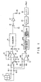
- FIG. 3 shows an example of the construction of a focus balance automatic adjusting device in a disk reproducing device according to a first embodiment of this invention.
- a four-divided detector 11 formed of photodiodes or the like is so designed that signals (currents) can be derived from four divided portions. Signal currents from the portions lying on the respective diagonal lines are added together and the results of addition are respectively supplied to current-voltage converters 31-1, 31-2 and to the inverting input terminal (-) and non-inverting input terminal (+) of a differential amplifier 13 via resistors R1, R2.
- the current-voltage converters 31-1, 31-2 convert the two added signal currents into voltages.
- the current-voltage converter 31-2 is designed such that the gain thereof can be converted and the gain thereof is controlled by a focus balance adjusting signal FB which will be described later.
- a parallel circuit of a resistor R3 and a capacitor C1 is connected between the inverting input terminal (-) and an output terminal of the differential amplifier 13. Further, a capacitor C2 and a resistor R7 is connected between the non-inverting input terminal (+) of the differential amplifier 13 and a ground terminal.
- An output of the differential amplifier 13 is supplied to a focus equalizer 15 as a focus error signal FE and the gain and phase thereof are compensated for by the equalizer 15. Whether the focus error signal FE is supplied to the equalizer 15 or not is controlled by use of a loop ON/OFF switch 14.
- the focus error signal FE is supplied to the equalizer 15, and when the switch 14 is set in the ON state, the potential of the input terminal of the equalizer 15 is set to the ground potential.
- a disturbance signal of stepped form (having first and second levels) created by a disturbance generator 32 is added to an output signal of the focus equalizer 15 and the result of addition is supplied to a selection switch 16.
- the selection switch 16 is switched to select the output signal of the equalizer 15 or a focus search signal FS and supplies a selected signal to a driver 17. Then, a focus actuator 18 is driven by the driver 17.
- Output signals of the current-voltage converters 31-1 and 31-2 are supplied to the inverting input terminal (-) of a differential amplifier 20 via resistors R4 and R5, respectively.
- a resistor R6 is connected between the inverting input terminal (-) and an output terminal of the differential amplifier 20 and the non-inverting input terminal (+) thereof is connected to the ground terminal.
- the differential amplifier 20 acts as an adder.
- a total sum signal of the four-divided detector 11 is derived by the adder, and as a result, an RF (radio frequency band) signal (which is also called an HF signal) which is information data is created.
- the RF signal is binary-coded by a data extraction circuit 22 and supplied to a signal processing circuit 23 as an EFM signal.
- the EFM demodulation, sub-code demodulation, error correction processing and the like are effected and the results of the processings are supplied to a digital/analog converter (DAC) 24 as data DA.
- DAC digital/analog converter
- An output of the DAC 24 is supplied to a low-pass filter (LPF) 25 and the high frequency component thereof is cut off. Then, an output of the LPF 25 is output as a reproduced audio signal A OUT .
- LPF low-pass filter
- the RF signal is supplied to a high-pass filter (HPF) and the D.C. component thereof is cut off.
- the high-pass filter is constructed by a differential amplifier 33, resistors R8, R9 and capacitor C3.
- One electrode of the capacitor C3 is connected to the output terminal of the differential amplifier 20 and the other electrode thereof is connected to one end of the resistor R8.
- the other end of the resistor R8 is connected to an inverting input terminal (-) of the differential amplifier 33.
- the resistor R9 is connected between the inverting input terminal (-) and an output terminal of the differential amplifier 33 and the non-inverting input terminal (+) of the differential amplifier 33 is connected to a ground terminal.
- An output of the differential amplifier 33 is supplied to an envelop detector circuit (detector) 34 to effect the peak detection and bottom detection and a difference therebetween is supplied to an analog/digital converter (ADC) 35 as an RFRP signal.
- ADC analog/digital converter
- the RFRP signal is converted into digital data by the ADC 35 and the digital data is supplied to a signal processing section 36.
- the signal processing section 36 is also supplied with a disturbance signal from the disturbance generator 32, receives values of the RFRP signal (digital signal) obtained when the disturbance signal is positive and negative, and derives a difference between the values thereof.
- An output of the signal processing section 36 is supplied to a pulse width modulation (PWM) circuit 37 to create a focus balance adjusting signal FB.
- PWM pulse width modulation
- the signal FB is supplied to the current-voltage converter 31-2 via a carrier rejection filter 38 formed of a resistor R14 and a capacitor C6 so as to control the gain.
- FIG. 4 shows an example of the detail construction of the envelop detection circuit 34.
- An RFRP signal is created based on the RF signal by the high-pass filter HPF and the envelop detection circuit 34.
- the envelop detection circuit 34 includes diodes D1, D2, current sources I1, I2, capacitors C4, C5, buffer amplifiers 26, 27, resistors R10 to R13, and differential amplifier 28.
- An output terminal of the differential amplifier 33 in the high-pass filter HPF is connected to the cathode of the diode D1 and the anode of the diode D2.
- the anode of the diode D1 is connected to an input terminal of the buffer amplifier 26 and the cathode of the diode D2 is connected to an input terminal of the buffer amplifier 27.
- the current source I1 is connected between the input terminal of the buffer amplifier 26 and the power source +Vcc and the capacitor C4 is connected between the input terminal thereof and the ground terminal.
- the current source I2 is connected between the input terminal of the buffer amplifier 27 and the power source -Vcc and the capacitor C5 is connected between the input terminal thereof and the ground terminal.
- An output terminal of the buffer amplifier 26 is connected to the non-inverting input terminal (+) of the differential amplifier 28 via a resistor R10, an output terminal of the buffer amplifier 27 is connected to one end of the resistor R11, and the other end of the resistor R11 is connected to the inverting input terminal (-) of the differential amplifier 28.
- a resistor R12 is connected between the non-inverting input terminal (+) of the differential amplifier 28 and the ground terminal and a resistor R13 is connected between the inverting input terminal (-) and an output terminal of the differential amplifier 28.
- An RFRP signal is derived from the output terminal of the differential amplifier 28.
- the value of a lower envelop of the RF signal is detected by means of the diode D1, current source I1, capacitor C4 and buffer amplifier 26 and the value of an upper envelop of the RF signal is detected by means of the diode D2, current source I2, capacitor C5 and buffer amplifier 27.
- An RFRP signal is created by deriving a difference between the above envelop values by use of the differential amplifier 28 and resistors R10 to R13.
- FIGS. 5 and 6 are diagrams each showing the relation between the de-focus amount and the amplitude of the RF signal.
- the de-focus amount of "0" indicates the position in which the focus position of the laser beam for the respective pickups is precisely set on the disk surface and the amplitude of the RF signal is set at the maximum level. If the focus position of the laser beam before adjustment is set at the point "B" of FIG. 5, the RF level (V) indicating the amplitude of the RF signal indicates a value of "A0". If, in this state, a disturbance signal as shown in FIG.
- the focus position is de-focused ("B+ds” and “B-ds") by “ds” with the point "B” set at the center.
- the amplitude of the RF signal becomes “Ap” when the de-focus amount is “B+ds” and it becomes “An” when the de-focus amount is “B-ds”.
- the levels of the RFRP signal corresponding to "Ap” and “An” of the RF signal are detected and the balance is adjusted to set the two levels equal to each other.
- the levels of the RFRP signal corresponding to "Ap” and “An” of the RF signal are set at "Apr” and "Anr" as shown in FIG.
- ds K ⁇ Gd ⁇ Vd/(1+HL) ( ⁇ m)
- the amplitude of the RF signal in the de-focus state becomes small.
- the operations of moving the focus position in a direction (positive) approaching the disk and in a direction (negative) departing from the disk are alternately effected and the gain of the first-stage current-voltage converter 31-2 is set to suppress the fluctuation in the amplitude of the RF signal at the respective times to a minimum as shown in FIG. 6.
- an RFRP signal which is a difference signal between the upper envelop and the lower envelop of the RF signal having amplitude information of the RF signal is used as a monitor signal.
- the RFRP signal is subjected to the AD conversion, a difference ⁇ L between the peak level of the RFRP signal at the time of positive side de-focus and the peak level of the RFRP signal at the time of negative side de-focus is derived, and the gain of the current-voltage converter 31-2 is adjusted to set the difference ⁇ L to "0".
- the tracking servo may be set in the ON or OFF state.
- the focus balance adjustment which was conventionally effected by the operator by use of the semi-fixed resistor or the like can be automatically effected. Further, the percent defective caused by the mis-adjustment in the mass production line of sets can be suppressed.
- the adjustment for the service condition of the set can be made and the adjustment deviation by deterioration of the pickup and electric parts with time can be prevented. Further, by adequately effecting the focus balance adjustment at the time of system operation, for example, the focus servo system can be set in the optimum condition according to the environment in which it is used.
- FIG. 8 illustrates a second embodiment of this invention and shows another example of the construction of the focus balance automatic adjustment device in the disk reproduction device.
- a four-divided detector 11 formed of photodiodes or the like is so designed that signals (currents) can be derived from four divided portions. Signals (currents) from the portions lying on each of the diagonal lines are added together and the results of addition are respectively supplied to current-voltage converters 12-1, 12-2 and to the inverting input terminal (-) and non-inverting input terminal (+) of a differential amplifier 39 via resistors R1, R2.
- the current-voltage converters 12-1, 12-2 each convert the two added signals (currents) into voltages.
- a parallel circuit of a resistor R3 and a capacitor C1 is connected between the inverting input terminal (-) and an output terminal of the differential amplifier 39. Further, a capacitor C2 and a resistor R7 are connected between the non-inverting input terminal (+) of the differential amplifier 39 and a ground terminal.
- the inverting input terminal (-) of the differential amplifier 39 is supplied with a focus balance adjustment signal FB output from a carrier rejection filter 38.
- a difference between the two signal currents output from the detector 11 can be derived by the differential amplifier 39 and difference signal is added to the focus balance adjustment signal FB to create a focus error signal FE.
- An output of the differential amplifier 39 is supplied to a focus equalizer 15 as a focus error signal FE and the gain and phase thereof are compensated for by the equalizer 15.
- the focus balance adjustment signal FB is added to the difference value of the signal current derived by the differential amplifier 39 for creating the focus error signal FE and thus the focus error signal is derived and used to effect the focus balance adjustment.
- the focus balance automatic adjustment device shown in FIG. 8 is different from the circuit of FIG. 3 in that the focus balance adjustment signal FB is added to the difference signal output from the differential amplifier 39 to create the focus error signal FE, but the other basic operation and effect are the same.
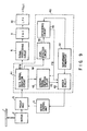
- FIG. 9 is a block diagram for illustrating a third embodiment of this invention and showing the schematic construction of a signal processing device having a focus balance automatic adjustment device and the peripheral unit thereof.
- the signal processing device 40 includes a data signal creation circuit 41, control signal creation circuit 42, adder circuit 43, level detection circuit 44, difference circuit 45 and disturbance generator 32.
- the data signal creation circuit 41 includes an adder constructed by the differential amplifier 20 and the resistors R4 to R6, and the current-voltage converters 31-1, 31-2 (or 12-1, 12-2) in the circuit shown in FIGS. 3 and 4.
- the control signal creation circuit 42 includes the differential amplifier 13 (or 39), resistors R1 to R3, R7, capacitors C1, C2, loop ON/OFF switch 14 and focus equalizer 15.
- the level detection circuit 44 includes the high-pass filter HPF and envelop detector circuit 34.
- the difference circuit 45 includes the ADC 35, signal processing section 36, PWM 37 and carrier rejection filter 38.
- the disk 1 having information recorded thereon is rotated by the motor 2.
- a laser beam which is generated from the semiconductor laser provided in the optical pickup unit 3 is applied to the disk 1, the reflected light is received by the four-divided detector in the unit 3, and current signals are derived from the four divided portions thereof.
- the current signals from the portions lying on each of the diagonal lines are added together.
- Two signals obtained by the addition are supplied to a data signal creation circuit 41. After the two signals supplied to the data signal creation circuit 41 are converted into voltages by the current-voltage converter, they are added together to create an RF signal, binary-coded and then supplied to a signal processing circuit 6 as an EFM signal.
- the EFM demodulation, sub-code demodulation, error correction process and the like are effected and an output thereof is supplied to a digital/analog converter (DAC) 9.
- An analog signal output from the DAC 9 is supplied to a low-pass filter (LPF) 10 and the high frequency component thereof is eliminated.
- a reproduction signal D OUT of data recorded on the disk 1 is output from the LPF 10.
- a signal supplied from the data signal creation circuit 41 to the control signal creation circuit 42 is added to a focus balance adjusting signal FB output from the difference circuit 45 to create a focus control signal FC (which is the same as the focus error FE of FIGS. 3 and 8) as a first control signal.
- the focus control signal FC is added to a disturbance signal having a first and second levels created by the disturbance generator 32 by the adder circuit 43 and the result of addition is supplied to the focus servo control circuit in the servo control unit 5.
- the focus servo control circuit drives the focus actuator in the pickup unit 3 to correct the focus position of the beam spot.
- a data signal (RF signal) created in the data signal creation circuit 41 is supplied to the level detection circuit 44.
- the first amplitude level of the data signal is detected according to the first level of the disturbance signal generated from the disturbance generator 32 by the circuit 44 and the second amplitude level of the data signal is detected according to the second level of the disturbance signal.
- An output of the level detection circuit 44 is supplied to the difference circuit 45 and a second control signal FB corresponding to a difference between the first and second amplitude levels of the data signal is created by the circuit 45.
- the second control signal FB is supplied to the control signal creation circuit 42 and a focus control signal FC is created according to the control signal FB by the circuit 42.
- the second control signal FB may be additionally supplied to the adder circuit 43 as indicated by broken lines in addition to the sum of the signal FC created by the control signal creation circuit 42 and the disturbance signal.
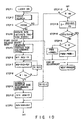
- FIG. 10 is a flowchart for illustrating the focus balance adjustment method effected by use of the control signal creation circuit 42, difference circuit 45, disturbance generator 32 and adder circuit 43 of the signal processing circuit shown in FIG. 9.
- the operation called the focus search is effected (STEP 2)
- the focus actuator is forcedly driven to a position near the focus position and the focus servo is closed.
- the focus servo is operated or not is determined (STEP 3) by monitoring the RF signal. If it is detected that the focus servo is operated, the disk 1 is rotated by the motor 2 (and the tracking servo is activated) to start the focus balance automatic adjustment (STEP 4).
- a positive disturbance signal is generated from the disturbance generator 32 (STEP 5) and supplied to the servo circuit. Then, an averaged number N is set to "1" and a register AVp used for calculating the average value is set to "0" (STEP 6). Next, Apr data is fetched and added to data of the register AVp (STEP 7). Then, whether the fetched sample number N is set to a value n 0 or not is checked (STEP 8), and if it is detected that the number is not set to n 0 , Apr data is repeatedly fetched.
- the disturbance signal is changed to the negative side (STEP 9), the averaged number N is set to "1", and a register AVn used for calculating the average number is initialized to "0" (STEP 10).
- Anr data items of n 0 are accumulatively added in the same manner as in the case of positive value (STEP 11, 12). After fetching Anr data items of n 0 , (Apr/Anr)/n 0 is calculated and a difference value D of the average level of RFRP signals for each sample is calculated (STEP 13). Then, whether the difference value D lies in the range of the window from "- ⁇ D" to "+ ⁇ D" or not is determined (STEP 14).
- the windows "- ⁇ D" and “+ ⁇ D” are minute values near "0" and " ⁇ D" are called the adjustment precision.
- control signal output from the PWM is subjected to the up/down control by one step at a time according to the sign of the value D.
- step (STEP 5) of generating the positive disturbance signal is effected again and the same process is repeatedly effected until the value D comes into the range of the window between "- ⁇ D" and "+ ⁇ D".
- the focus balance automatic adjustment operation is effected as described above, and after the completion of the process, the next process including data fetch is effected.
- the focus balance automatic adjustment device in the disk reproducing device of this invention since the positive and negative de-focus positions are formed according to a disturbance signal output from the disturbance generator and a difference between them is calculated each time the central position thereof is moved, time required for the adjustment becomes shorter as the initial condition is nearer to the final adjustment point and thus the adjustment time can be reduced.
- the adjustment is started by the disturbance signal from the disturbance generator 32, the position in which the focus position is set on the parabolic curve of the de-focus characteristic can be determined. Therefore, by de-focusing the focus position by a minute amount in the positive direction and negative direction from the above position, the direction towards the adjustment point can be determined according to whether the two difference values are positive or negative. Further, since only determination whether a difference value between RF signals fetched in the two de-focus conditions is "0" or not is made, the circuit construction can be made simple and the processing time can be reduced.
Landscapes
- Optical Recording Or Reproduction (AREA)
Claims (11)
- Appareil d'ajustement automatique d'équilibrage de focalisation, comprenant
un dispositif d'ajustement de foyer (31-1, 31-2, 13, 14, 15, 16, 17, 18) destiné à ajuster la position du foyer d'un faisceau lumineux dans une unité formant capteur optique pour la lecture d'informations enregistrées sur un disque par application d'un faisceau lumineux au disque et réception de la lumière réfléchie,
un dispositif (37, 38) de réglage de foyer destiné à créer un signal de commande du dispositif d'ajustement de foyer (31-1, 31-2, 13, 14, 15, 16, 17, 18),
un dispositif (32) générateur d'un signal de perturbation destiné à créer un signal de perturbation ayant un premier et un second niveau destinés à écarter la position du foyer du faisceau lumineux dans des directions opposées,
un dispositif (20, R4 à R6) de détection de niveau destiné à détecter les niveaux des signaux de sortie de l'unité formant capteur créés lorsque le premier et le second niveau du signal de perturbation sont transmis,
un dispositif (C3, R8, R9, 33, 34) de dérivation de différence de niveau destiné à dériver une différence entre le niveau de sortie de l'unité formant capteur optique détecté par le dispositif de détection de niveau (20, R4 à R6) lorsque le signal de perturbation est mis à un premier niveau et le signal de sortie de l'unité formant capteur optique détecté lorsque le signal de perturbation est établi à un second niveau, et
un dispositif (35, 36) de traitement de signaux destiné à commander le dispositif (37, 38) de réglage de foyer en fonction de la différence de niveau transmise par le dispositif de dérivation de différence de niveau (HPF, 34),
dans lequel
le dispositif de dérivation de différence de niveau (C3, R8, R9, 33, 34) comprend un filtre passe-haut (HPF) destiné à éliminer la composante en courant continu du signal de sortie du dispositif de détection de niveau (20, R4 à R6) et un circuit de détection d'enveloppe (34), le circuit de détection d'enveloppe (34) ayant une première section de circuit (D1, 11, C4) destinée à effectuer la détection de crête du filtre passe-haut (HPF), une seconde section de circuit (D2, I2, C5) destinée à effectuer une détection inférieure du filtre passe-haut (HPF), et une troisième section de circuit (28, R11-R13 destinée à créer un signal RFRP par dérivation de la différence de valeur entre une enveloppe supérieure d'un signal RF transmis par la première section de circuit et un signal inférieur d'enveloppe correspondant provenant de la seconde section de circuit,
le dispositif de traitement de signaux (35, 36) comprend un convertisseur analogique-numérique (35) destiné à transformer le signal RFRP transmis par la troisième section de circuit (28, R11-R13) en un signal numérique, et une section de traitement de signaux (36) destinée à recevoir les signaux RFRP du convertisseur analogique-numérique (35) lorsque le signal de perturbation est placé du côté positif et du côté négatif et à dériver la différence de niveau de crête entre le signal RFRP au moment de la défocalisation du côté positif et le signal RFRP au moment de la défocalisation du côté négatif,
le dispositif de traitement de signaux (35, 36) établit le niveau de sortie de l'unité formant capteur optique obtenu lorsque le signal de perturbation est placé au premier niveau et le niveau de sortie de l'unité formant capteur obtenu lorsque le signal de perturbation est réglé au second niveau à des valeurs égales,
le dispositif de commande (37, 38) comprend un circuit (37) de modulation par impulsions de largeur variable destiné à soumettre un signal de sortie de la section de traitement de signaux (36) à la modulation par impulsions de largeur variable pour la création d'un signal d'ajustement d'équilibrage de focalisation comme signal de commande, et
le dispositif d'ajustement de foyer (31-1, 31-2, 13, 14, 15, 16, 17, 18) comprend un premier et un second convertisseurs courant-tension (31-1, 31-2) destinés à amplifier les informations enregistrées lues par l'unité formant capteur optique, le second convertisseur courant-tension (31-2) étant commandé par le signal d'ajustement d'équilibrage de focalisation (FB) transmis par le circuit (37) de modulation par impulsions de largeur variable afin que la différence de niveau de crête entre le signal RFRP au moment d'une défocalisation du côté positif et le signal RFRP au moment de la défocalisation du côté négatif devienne nulle. - Appareil d'ajustement automatique d'équilibrage de focalisation selon la revendication 1, caractérisé en ce que l'unité formant capteur optique comprend un détecteur (11) divisé en quatre.
- Appareil d'ajustement automatique d'équilibrage de focalisation selon la revendication 2, caractérisé en ce que
le premier convertisseur courant-tension (31-1) reçoit le résultat de l'addition de courants de signalisation dérivés de parties qui se trouvent sur l'une des diagonales du détecteur divisé en quatre (11), et
le second convertisseur courant-tension (31-2) reçoit le résultat de l'addition des courants de signalisation dérivés de parties qui se trouvent sur l'autre diagonale du détecteur divisé en quatre (11), et en ce que
le dispositif d'ajustement de foyer comporte en outre
un amplificateur différentiel (13) qui reçoit les signaux de sortie des premier et second convertisseurs courant-tension (31-1, 31-2) pour la création d'un signal d'erreur de focalisation (FE),
un égaliseur de focalisation (15) destiné à recevoir le signal d'erreur de focalisation (FE) pour compenser le gain et la phase,
un dispositif additionneur destiné à ajouter un signal de sortie de l'égaliseur de focalisation (15) et le signal de perturbation créé par le dispositif (32) générateur du signal de perturbation, et
un circuit de pilotage (17) destiné à piloter un organe de manoeuvre de foyer (18) en fonction d'un signal de sortie du dispositif additionneur. - Appareil d'ajustement automatique d'équilibrage de focalisation selon la revendication 3, caractérisé en ce que l'amplificateur différentiel (39) dérive une valeur de différence entre les courants de signalisation des signaux de sortie des premier et second convertisseurs courant-tension (12-1, 12-2) et ajoute la valeur de la différence à un signal de sortie du dispositif de réglage de foyer (37, 38) pour la création du signal d'erreur de focalisation (FE).
- Appareil d'ajustement automatique d'équilibrage de focalisation selon la revendication 3 ou 4, caractérisé en ce qu'il comprend en outre un interrupteur de boucle (14) destiné à commander la transmission ou non du signal d'erreur de focalisation (FE) à l'égaliseur de focalisation (15).
- Appareil d'ajustement automatique d'équilibrage de focalisation selon la revendication 3 ou 4, caractérisé en ce qu'il comprend en outre un commutateur de sélection (16) destiné à transmettre sélectivement un signal parmi le signal de sortie du dispositif additionneur et le signal de recherche de foyer (FS) au circuit de pilotage (17).
- Appareil d'ajustement automatique d'équilibrage de focalisation selon l'une quelconque des revendications 2 à 6, caractérisé en ce que le dispositif de détection de niveau comprend un additionneur (20) destiné à dériver la somme totale du détecteur divisé en quatre (11) et à transmettre un signal RF qui représente des données d'informations.
- Appareil d'ajustement automatique d'équilibrage de focalisation selon l'une quelconque des revendications 3 à 7, caractérisé en ce que le dispositif (37, 38) de réglage de foyer comporte en outre un filtre éliminateur de porteuse (38) destiné à recevoir un signal d'ajustement d'équilibrage de focalisation provenant du circuit (37) de modulation par impulsions de largeur variable pour la création d'un signal utilisé pour le réglage du gain du second convertisseur courant-tension (31-2).
- Appareil de reproduction sur disque, comprenant un appareil d'ajustement automatique d'équilibrage de focalisation selon l'une quelconque des revendications précédentes, caractérisé en ce que
l'appareil comporte en outre un dispositif (5) de commande asservie destiné à régler la position du foyer dans l'unité formant capteur (3) d'après des informations lues sur le disque (1), le dispositif de commande asservie (5) reçoit un signal de sortie d'un dispositif additionneur (43) destiné à ajouter le signal de commande et le signal de perturbation ou à ajouter le signal de commande, le signal de perturbation et le signal de différence. - Appareil de traitement de signaux comprenant un appareil de reproduction sur disque selon la revendication 9.
- Procédé d'ajustement automatique d'équilibrage de focalisation destiné à ajuster la position du foyer d'un faisceau lumineux dans une unité formant capteur optique destinée à lire des informations enregistrées sur un disque par application d'un faisceau lumineux au disque et réception de la lumière réfléchie, comprenant
une étape de création d'un signal de perturbation d'un premier niveau,
une étape de transmission du signal de perturbation du premier niveau à l'unité à disque optique pour que la position du foyer du faisceau lumineux soit déviée dans une première direction,
une étape de détection d'un premier niveau d'amplitude d'un signal de sortie de l'unité formant capteur optique obtenu lorsque le signal de perturbation du premier niveau est transmis,
une étape d'élimination de la composante en courant continu du signal de sortie obtenu lorsque le signal de perturbation du premier niveau est transmis à l'aide d'un filtre passe-haut (HPF),
une étape de création d'un signal de perturbation d'un second niveau,
une étape de transmission du signal de perturbation du second niveau à l'unité formant capteur optique afin que la position du foyer et du faisceau lumineux s'écarte dans une seconde direction opposée à la première direction,
une étape de détection d'un second niveau d'amplitude d'un signal de sortie d'une unité formant capteur optique obtenu lorsque le signal de perturbation du second niveau est transmis,
une étape d'élimination de la composante en courant continu du signal de sortie obtenu lorsque le signal de perturbation du second niveau est transmis à l'aide d'un filtre passe-haut (HPF),
l'exécution d'une détection d'enveloppe du signal de sortie du filtre passe-haut (HPF) à l'aide d'une première section de circuit (D1, I1, C4) destinée à assurer la détection de crête du filtre passe-haut (HPF), une seconde section de circuit (D2, I2, C5) étant destinée à effectuer une détection inférieure du filtre passe-haut (HPF),
une étape de création, avec une troisième section de circuit (28, R11-R13), d'un signal RFRP, par dérivation d'une différence de valeur entre une enveloppe supérieure d'un signal RF transmis par la première section de circuit et une enveloppe inférieure correspondante transmise par la seconde section de circuit,
une étape de conversion, par un convertisseur analogique-numérique (35), du signal RFRP transmis par la troisième section de circuit (28, R11-R13) en un signal numérique,
une étape de réception de signaux RFRP du convertisseur analogique-numérique (35) lorsque le signal de perturbation est établi du côté positif et du côté négatif, et de dérivation de la différence de niveau de crête entre le signal RFRP au moment de la délocalisation du côté positif et du signal RFRP au moment de la défocalisation du côté négatif,
une étape de correction de la position de focalisation du faisceau lumineux appliqué par l'unité formant capteur optique, par utilisation d'un premier et d'un second convertisseur courant-tension destinés à transformer un signal de courant transmis de l'unité formant capteur optique en un signal de tension afin que la différence de niveau de crête entre le signal RFRP au moment de la défocalisation du côté positif et le signal RFRP au moment de la défocalisation du côté négatif devienne nulle, et
une étape de détermination du fait que le faisceau lumineux de l'unité formant capteur optique est focalisé lorsque le premier et second niveau d'amplitude sont réglés à des valeurs égales.
Applications Claiming Priority (3)
| Application Number | Priority Date | Filing Date | Title |
|---|---|---|---|
| JP47119/93 | 1993-02-15 | ||
| JP5047119A JPH06243496A (ja) | 1993-02-15 | 1993-02-15 | ディスク再生装置及びそのフォーカスバランス自動調整方法及び信号処理装置 |
| JP4711993 | 1993-02-15 |
Publications (2)
| Publication Number | Publication Date |
|---|---|
| EP0612063A1 EP0612063A1 (fr) | 1994-08-24 |
| EP0612063B1 true EP0612063B1 (fr) | 2002-11-06 |
Family
ID=12766280
Family Applications (1)
| Application Number | Title | Priority Date | Filing Date |
|---|---|---|---|
| EP94102288A Expired - Lifetime EP0612063B1 (fr) | 1993-02-15 | 1994-02-15 | Dispositif et méthode d'équilibrage automatique d'un détecteur d'écart de focalisation |
Country Status (5)
| Country | Link |
|---|---|
| US (1) | US5610886A (fr) |
| EP (1) | EP0612063B1 (fr) |
| JP (1) | JPH06243496A (fr) |
| KR (1) | KR100187795B1 (fr) |
| DE (1) | DE69431638T2 (fr) |
Families Citing this family (22)
| Publication number | Priority date | Publication date | Assignee | Title |
|---|---|---|---|---|
| US5761164A (en) * | 1993-11-15 | 1998-06-02 | Pioneer Electronic Corporation | Gain control device for servo control |
| US5682372A (en) * | 1995-08-22 | 1997-10-28 | Sony Corporation | Method and apparatus for playing back multilayer disk |
| JPH09237424A (ja) * | 1995-12-26 | 1997-09-09 | Pioneer Electron Corp | フォーカスエラー信号のバイアス量制御装置 |
| US6028826A (en) * | 1996-09-18 | 2000-02-22 | Matsushita Electric Industrial Co., Ltd. | Optical disk apparatus performing correction of phase difference tracking error signal, adjustment of focus position and process of gain adjustment |
| US6252835B1 (en) | 1996-09-19 | 2001-06-26 | L G Electronics Inc | Apparatus for automatically adjusting focus offset and method thereof in a disc player |
| KR100447663B1 (ko) * | 1996-09-19 | 2004-11-08 | 엘지전자 주식회사 | Cdp포커스오프셋자동조정장치및그방법 |
| JPH1173657A (ja) * | 1997-06-27 | 1999-03-16 | Pioneer Electron Corp | フォーカス制御装置及び方法 |
| JP3688452B2 (ja) * | 1997-11-20 | 2005-08-31 | パイオニア株式会社 | 制御偏差検出装置及び制御装置 |
| US6178145B1 (en) | 1997-11-26 | 2001-01-23 | Kabushiki Kaisha Toshiba | Focus servo control system and disk reproducing system |
| TW396337B (en) * | 1998-02-13 | 2000-07-01 | Mediatek Inc | The automatic regulating device of cdrom optimum focusing spot and the method thereof |
| CN1115689C (zh) * | 1998-02-26 | 2003-07-23 | 联发科技股份有限公司 | 光盘机最佳聚焦点自动调整装置与方法 |
| KR100585055B1 (ko) * | 1998-05-12 | 2006-09-12 | 삼성전자주식회사 | 광학 시스템의 디펙트 검출장치 및 방법 |
| JP3736666B2 (ja) * | 1999-04-14 | 2006-01-18 | パイオニア株式会社 | チルトサーボ装置及び制御方法 |
| JP3728390B2 (ja) * | 1999-10-08 | 2005-12-21 | パイオニア株式会社 | フォーカスサーボ制御装置並びに情報再生装置及び情報記録装置 |
| TW484128B (en) * | 2000-01-12 | 2002-04-21 | Sony Corp | Optical disc apparatus |
| US6912190B2 (en) * | 2000-11-15 | 2005-06-28 | Matsushita Electric Industrial Co., Ltd. | Optical disc apparatus and method for reading information from an optical disk having tracks and spaces between the tracks on which address information is recorded |
| US7992067B1 (en) * | 2001-11-09 | 2011-08-02 | Identita Technologies International SRL | Method of improving successful recognition of genuine acoustic authentication devices |
| JP3974447B2 (ja) * | 2002-05-08 | 2007-09-12 | アルパイン株式会社 | 光ディスク再生装置及び光ディスク再生装置の自動調整方法 |
| KR100767132B1 (ko) | 2006-03-23 | 2007-10-12 | 엘지전자 주식회사 | 광디스크장치의 포커스 위치 조정방법 |
| TW200837732A (en) * | 2006-10-09 | 2008-09-16 | Koninkl Philips Electronics Nv | Optimizing a parameter for reading-out/recording of an optical data carrier |
| JP2008123567A (ja) | 2006-11-08 | 2008-05-29 | Funai Electric Co Ltd | 光ディスク装置、フォーカスバランスの調整方法 |
| US7778120B2 (en) * | 2007-05-08 | 2010-08-17 | Mediatek Inc. | Calibration method for determining servo parameters for accessing an optical disc |
Family Cites Families (10)
| Publication number | Priority date | Publication date | Assignee | Title |
|---|---|---|---|---|
| CA1261467A (fr) * | 1985-11-28 | 1989-09-26 | Akira Minami | Dispositif de commande de servomecanisme de focalisation pour lecteur de disques optiques a reglage du decalage |
| JPH056575Y2 (fr) * | 1986-04-18 | 1993-02-19 | ||
| JPH0760527B2 (ja) * | 1986-09-17 | 1995-06-28 | パイオニア株式会社 | 光学式ピックアップ装置 |
| JP2615930B2 (ja) * | 1988-10-27 | 1997-06-04 | 松下電器産業株式会社 | フォーカスバランス自動調整装置 |
| JPH02265025A (ja) * | 1989-04-05 | 1990-10-29 | Pioneer Electron Corp | サーボループのループゲイン設定方法 |
| JPH033121A (ja) * | 1989-05-31 | 1991-01-09 | Matsushita Electric Ind Co Ltd | 光ディスク記録再生装置 |
| JPH03108128A (ja) * | 1989-09-21 | 1991-05-08 | Olympus Optical Co Ltd | 光学式情報記録再生装置 |
| JPH03263620A (ja) * | 1990-03-13 | 1991-11-25 | Pioneer Electron Corp | ディスクプレーヤのサーボ装置 |
| US5164932A (en) * | 1990-09-28 | 1992-11-17 | International Business Machines Corporation | Acquiring a best focus using a focus signal offset |
| JP2716610B2 (ja) * | 1991-10-16 | 1998-02-18 | 三菱電機株式会社 | フォーカス制御装置 |
-
1993
- 1993-02-15 JP JP5047119A patent/JPH06243496A/ja active Pending
-
1994
- 1994-02-14 KR KR1019940002527A patent/KR100187795B1/ko not_active Expired - Fee Related
- 1994-02-15 DE DE69431638T patent/DE69431638T2/de not_active Expired - Fee Related
- 1994-02-15 EP EP94102288A patent/EP0612063B1/fr not_active Expired - Lifetime
-
1995
- 1995-12-19 US US08/579,035 patent/US5610886A/en not_active Expired - Lifetime
Also Published As
| Publication number | Publication date |
|---|---|
| US5610886A (en) | 1997-03-11 |
| JPH06243496A (ja) | 1994-09-02 |
| DE69431638T2 (de) | 2003-07-03 |
| EP0612063A1 (fr) | 1994-08-24 |
| KR100187795B1 (ko) | 1999-06-01 |
| DE69431638D1 (de) | 2002-12-12 |
Similar Documents
| Publication | Publication Date | Title |
|---|---|---|
| EP0612063B1 (fr) | Dispositif et méthode d'équilibrage automatique d'un détecteur d'écart de focalisation | |
| US6304536B1 (en) | Optical disk apparatus | |
| EP0840297B1 (fr) | Circuit de détection de piste pour lecteur de disque optique | |
| US6510112B1 (en) | Drive apparatus for optical recording medium | |
| EP0423731A2 (fr) | Dispositif d'accès aux pistes et dispositif de suivi de piste | |
| JPH06295458A (ja) | 光学式情報記録再生装置 | |
| US4661942A (en) | Control apparatus for information storage and retrieval system | |
| US6560173B2 (en) | Servo control apparatus for optical disc player | |
| US5703849A (en) | Tracking servo correction control circuit | |
| JPH11161978A (ja) | 光学ピックアップ及び/又は光ディスクのフォーカス特性測定装置、光学ピックアップ及び/又は光ディスクのフォーカス特性測定方法、光ディスクの記録及び/又は再生装置、並びに、光ディスクの記録及び/又は再生方法 | |
| US6198085B1 (en) | Repeat control apparatus, information reproducing apparatus and information recording apparatus | |
| US7158455B2 (en) | Servo error detecting device for optical disk | |
| KR100486271B1 (ko) | 트랙킹 에러신호 생성 장치 및 방법 | |
| JPH07254156A (ja) | 光ディスク及び光ディスク再生装置の信号処理回路 | |
| KR100285633B1 (ko) | 광디스크 장치의 트랙 서보 제어방법 및 장치 | |
| KR100556495B1 (ko) | 광 디스크 기록 재생 방법 및 장치 | |
| KR0149342B1 (ko) | 밸런스 자동조정기능을 갖는 광디스크 플레이어의 트래킹 에러 검출회로 | |
| US20060209621A1 (en) | Optical disk recording/reproducing apparatus | |
| KR100303214B1 (ko) | 광디스크 포커스 서보계의 자동 이득 조정방법 및 장치 | |
| JP2935930B2 (ja) | フォーカスサーボのバランス調整装置 | |
| JP2878974B2 (ja) | 光ディスク再生装置 | |
| JPH10208247A (ja) | 光ディスク装置、レーザ光の補正方法、光ディスク装置のトラッキング信号補正方法、光ディスク装置のフォーカッシング信号補正方法 | |
| US20060007802A1 (en) | Optical disk reproducing device | |
| JPH04245035A (ja) | 光学的情報記録再生装置 | |
| KR19990015239A (ko) | 트랙 밸런스 자동조정장치 |
Legal Events
| Date | Code | Title | Description |
|---|---|---|---|
| PUAI | Public reference made under article 153(3) epc to a published international application that has entered the european phase |
Free format text: ORIGINAL CODE: 0009012 |
|
| 17P | Request for examination filed |
Effective date: 19940215 |
|
| AK | Designated contracting states |
Kind code of ref document: A1 Designated state(s): DE FR GB |
|
| 17Q | First examination report despatched |
Effective date: 19980605 |
|
| GRAG | Despatch of communication of intention to grant |
Free format text: ORIGINAL CODE: EPIDOS AGRA |
|
| GRAG | Despatch of communication of intention to grant |
Free format text: ORIGINAL CODE: EPIDOS AGRA |
|
| GRAH | Despatch of communication of intention to grant a patent |
Free format text: ORIGINAL CODE: EPIDOS IGRA |
|
| GRAH | Despatch of communication of intention to grant a patent |
Free format text: ORIGINAL CODE: EPIDOS IGRA |
|
| GRAA | (expected) grant |
Free format text: ORIGINAL CODE: 0009210 |
|
| AK | Designated contracting states |
Kind code of ref document: B1 Designated state(s): DE FR GB |
|
| REG | Reference to a national code |
Ref country code: GB Ref legal event code: FG4D |
|
| REF | Corresponds to: |
Ref document number: 69431638 Country of ref document: DE Date of ref document: 20021212 |
|
| ET | Fr: translation filed | ||
| PLBE | No opposition filed within time limit |
Free format text: ORIGINAL CODE: 0009261 |
|
| STAA | Information on the status of an ep patent application or granted ep patent |
Free format text: STATUS: NO OPPOSITION FILED WITHIN TIME LIMIT |
|
| 26N | No opposition filed |
Effective date: 20030807 |
|
| PGFP | Annual fee paid to national office [announced via postgrant information from national office to epo] |
Ref country code: DE Payment date: 20070208 Year of fee payment: 14 |
|
| PGFP | Annual fee paid to national office [announced via postgrant information from national office to epo] |
Ref country code: GB Payment date: 20070214 Year of fee payment: 14 |
|
| PGFP | Annual fee paid to national office [announced via postgrant information from national office to epo] |
Ref country code: FR Payment date: 20070208 Year of fee payment: 14 |
|
| GBPC | Gb: european patent ceased through non-payment of renewal fee |
Effective date: 20080215 |
|
| REG | Reference to a national code |
Ref country code: FR Ref legal event code: ST Effective date: 20081031 |
|
| PG25 | Lapsed in a contracting state [announced via postgrant information from national office to epo] |
Ref country code: DE Free format text: LAPSE BECAUSE OF NON-PAYMENT OF DUE FEES Effective date: 20080902 |
|
| PG25 | Lapsed in a contracting state [announced via postgrant information from national office to epo] |
Ref country code: FR Free format text: LAPSE BECAUSE OF NON-PAYMENT OF DUE FEES Effective date: 20080229 |
|
| PG25 | Lapsed in a contracting state [announced via postgrant information from national office to epo] |
Ref country code: GB Free format text: LAPSE BECAUSE OF NON-PAYMENT OF DUE FEES Effective date: 20080215 |