EP0612151B1 - Halbleitervorrichtung zur Reduzierung einer Taktverschiebung in einer Vielfalt von Mustern von Verdrahtungsblöcken - Google Patents
Halbleitervorrichtung zur Reduzierung einer Taktverschiebung in einer Vielfalt von Mustern von Verdrahtungsblöcken Download PDFInfo
- Publication number
- EP0612151B1 EP0612151B1 EP94102242A EP94102242A EP0612151B1 EP 0612151 B1 EP0612151 B1 EP 0612151B1 EP 94102242 A EP94102242 A EP 94102242A EP 94102242 A EP94102242 A EP 94102242A EP 0612151 B1 EP0612151 B1 EP 0612151B1
- Authority
- EP
- European Patent Office
- Prior art keywords
- wiring
- clock signal
- wirings
- lattice
- center portion
- Prior art date
- Legal status (The legal status is an assumption and is not a legal conclusion. Google has not performed a legal analysis and makes no representation as to the accuracy of the status listed.)
- Expired - Lifetime
Links
Images



Classifications
-
- H—ELECTRICITY
- H03—ELECTRONIC CIRCUITRY
- H03K—PULSE TECHNIQUE
- H03K19/00—Logic circuits, i.e. having at least two inputs acting on one output; Inverting circuits
- H03K19/003—Modifications for increasing the reliability for protection
- H03K19/00323—Delay compensation
-
- G—PHYSICS
- G06—COMPUTING OR CALCULATING; COUNTING
- G06F—ELECTRIC DIGITAL DATA PROCESSING
- G06F1/00—Details not covered by groups G06F3/00 - G06F13/00 and G06F21/00
- G06F1/04—Generating or distributing clock signals or signals derived directly therefrom
- G06F1/10—Distribution of clock signals, e.g. skew
Definitions
- This invention relates to a semiconductor device which may be incorporated in an LSI circuit or the like.
- a conventional semiconductor device of the type described comprises a large number of electronic elements, such as flip-flops, and the like, and a clock driver which delivers clock signals to the electronic elements through a wiring pattern between the electronic elements and the clock driver.
- the clock signals are delivered to all of the electronic elements without any difference of a delay time, namely, a delay time difference.
- a delay time difference is generally called a clock skew.
- the wiring pattern is formed into a lattice-shape.
- a lattice-shaped wiring pattern is exemplified in Unexamined Japanese Patent Publication No. Shô 63-107316, namely, 107316/1988, and in EP-A-0 501 652, which discloses a so-called balanced tree clock distribution network for an integrated circuit.
- the clock skew becomes large with an increase of the integration scale, which causes the error operation to frequently occur.
- a semiconductor device as defined in claim 1.
- a clock signal distribution network as defined in claim 5.
- Preferred embodiments of the present invention are defined independent claims 2 to 4 and 6.
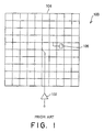
- a conventional semiconductor device will first be described for a better understanding of this invention.
- the conventional semiconductor device is substantially equivalent to that disclosed in the above publication referenced by the preamble of the instant specification.
- the conventional semiconductor device 100 comprises a clock driver 102 which provides clock signals of a predetermined frequency, for example, 2 GHz, a wiring pattern 104 connected to the clock driver 102, and a plurality of electronic elements 106, such as filp-flops, which are connected to the wiring pattern 104 and which are operable in timed relation to the clock signals.
- a clock driver 102 which provides clock signals of a predetermined frequency, for example, 2 GHz
- a wiring pattern 104 connected to the clock driver 102
- a plurality of electronic elements 106 such as filp-flops
- the clock signals which are generated by a clock signal oscillator are sent through the clock driver 102 to be given to the electronic elements 106 through the wiring pattern 104.
- a clock skew might become large with an increase of the chip size and which an extension of the wiring pattern 104. This results in an increase of an error operation caused to occur by a timing error. No suggestion is made at all about an increase of a clock skew which brings about the timing error.
- a semiconductor device 200 comprises a clock driver 102 which provides clock signals of a predetermined frequency, for example, 2 GHz, like in Fig. 1.
- the illustrated semiconductor device 200 comprises a plurality of wiring blocks 104' each of which has lattice-shaped wirings, as specified in Fig. 2 by a block located at an uppermost row and a leftmost column, and which may be similar to the wiring pattern 104 illustrated in Fig. 1.
- each of the wiring blocks 104' has a block center portion 104'a and a plurality of electronic elements 106, such as flip-flops, and the like, connected to the lattice-shaped wirings.
- the block center 104'a is located at a center of the lattice-shaped wirings in the illustrated example.
- an interconnecting wiring pattern (collectively depicted at 208) is laid between the respective wiring blocks 104' and the clock driver 102.
- the electronic elements 106 of each wiring block 104' are connected to the clock driver 102 through the interconnecting wiring pattern 208.
- the illustrated interconnecting wiring pattern 208 is divided into a plurality of subsidiary wiring patterns 208A, 208b, 208c, 208d, 208e, and 208f, each of which has a capital H-shape.
- the subsidiary wiring pattern 208A is directly connected to the clock driver 102 at a center point of the subsidiary wiring pattern, namely, the H-shape 208A and is connected at four ends of the H-shape to the remaining subsidiary wiring patterns 208b to 208f.
- Each of the remaining subsidiary wiring patterns 208b to 208f is connected at four ends of each H-shape to four block centers of, such as 104'a, of the wiring blocks 104'.
- the interconnecting wiring pattern 208 serves to connect the clock driver 102 to the respective block centers 104'a so that the distances between the clock driver 102 and the respective block centers 104'a are substantially equal to one another.
- the electronic elements 106 are connected through a plurality of additional wiring patterns 210 to each wiring block 104'.
- Each of the additional wiring patterns 210 may include a plurality of buffer circuits 212.
- Each electronic element 106 has a clock signal input terminal C1 which is connected to an optional point of each lattice-shaped wiring blocks 104' through each buffer circuit 212 by a wiring of short length.
- each of the lattice-shaped wiring blocks 104' be implemented by a multilayer structure.
- the multilayer structure is formed by a first layer for the electronic elements, a second layer for the wirings extended towards a row direction, namely, an X-direction, and a third layer for the wirings extended towards a column direction, namely, a Y-direction.
- the wirings in the X-direction and the wirings in the Y-direction are connected to one another on each lattice point by way of throughholes (not shown).
- each of the lattice-shaped wiring blocks 104' practically consists of 18 x 18 wirings.
- Each wiring is made of gold and is arranged at a pitch of 300 micronmeters defined between two adjacent ones of the wirings.
- Each wiring has a width of 1 micronmeter and a thickness of 0.7 micronmeter.
- a clock skew which might result from the additional wiring patterns 210 can be decreased because a floating capacitance C is balanced.
- a clock skew in a square area of 5.4 mm x 5.4 mm can be decreased to substantially 55 psec, on the assumption that the clock skew due to the additional wiring patterns 210 is equal to 10 psec.
- a capacitance of each lattice-shaped wiring block 104' is 13.2 pF while the floating capacitance of the terminal C1 and the electronic element 106 is, for example, 15 fF or so. Therefore, the former is considerably greater than the latter. Consequently, a total capacitance of each lattice-shaped wiring block 104' and any clock signal wiring connected thereto can be deemed to be substantially equal to one another.
- the interconnecting wiring pattern 208 connects the clock driver 102 with the block center portions 104'a so that the distance between the clock driver 102 and each of the block centers 104'a is substantially equal to one another in the center portions 104'a.
- the clock skew between each block center 104'a and the clock driver 102 can be extremely decreased.
- the semiconductor device 300 has a structure similar to that of the semiconductor device 200 illustrated in Fig. 2 except that the semiconductor device 300 further comprises a plurality of buffer circuits 312 each of which is incorporated in the interconnecting wiring pattern 208.
- the buffer circuits 312 is located between the end points of the subsidiary wiring pattern 208A and the centers of the remaining subsidiary wiring patterns 208b to 208f. Similar parts are designated by like reference numerals.
- a load imposed on the clock driver 102 is considerably lightened, since each lattice-shaped wiring block 104' is driven by each buffer circuit 312.
- the clock driver 102 can be designed to be small in size.
- Such a clock driver 102 of a small size brings about a reduction of noise and a reduction of current consumption.
- an additional power supply is unnecessary to drive each lattice-shaped wiring block 104'.
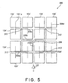
- the semiconductor device 400 has a structure similar to that of the semiconductor device 200 illustrated in Fig. 2 except that the interconnecting wiring pattern 208' comprises a plurality of subsidiary wiring patterns 208'A, 208'b, 208'c, 208'd, 208'e, and 208'f each of which has a lattice-shape, namely, a square shape.
- a resistance of each subsidiary wiring pattern 208'b, 208'c, 208'd, 208'e, and 208'f becomes equal to one another, like the first embodiment mentioned above. Furthermore, the resistance of each subsidiary wiring pattern 208'A, 208'b, 208'c, 208'd, 208'e, and 208'f becomes smaller than that of each subsidiary wiring pattern 208A, 208b, 208c, 208d, 208e, and 208f (shown in Fig. 2) which has the H-shape. It is possible to keep the resistance of each of the wiring patterns 208A, 208b to 208f substantially equal to one another. In other words, variation of the resistances among the wiring patterns can be minimized.
- the semiconductor device 400 may further comprise a plurality of buffer circuits each of which is incorporated in the interconnecting wiring patterns 208'.
- the electronic elements are not restricted to flip-flops and may be, for example, registers, shift registers, and the like.
Landscapes
- Engineering & Computer Science (AREA)
- Physics & Mathematics (AREA)
- General Engineering & Computer Science (AREA)
- Theoretical Computer Science (AREA)
- Computer Hardware Design (AREA)
- Computing Systems (AREA)
- Mathematical Physics (AREA)
- General Physics & Mathematics (AREA)
- Design And Manufacture Of Integrated Circuits (AREA)
- Semiconductor Integrated Circuits (AREA)
Claims (6)
- Halbleitervorrichtung mit:wobei die gitterförmigen Verdrahtungsblöcke jeweils eine erste Anzahl von parallelen Verdrahtungen, eine zweite Anzahl von parallelen Verdrahtungen und eine Umfangsverdrahtung aufweisen; wobei die ersten und zweiten Anzahlen von parallelen Verdrahtungen jeweils erste und zweite Enden haben; wobei die erste Anzahl von parallelen Verdrahtungen rechtwinkelig zu der zweiten Anzahl von parallelen Verdrahtungen liegt und ein Gitter definiert mit einem elektrischen Anschluß, der an den Schnittpunkten der Verdrahtungen der ersten Anzahl paralleler Verdrahtungen mit den Verdrahtungen von der zweiten Anzahl paralleler Verdrahtungen ausgeformt ist; wobei die Umfangsverdrahtung um die ersten und zweiten Anzahlen von parallelen Verdrahtungen angeordnet ist und mit den ersten und zweiten Enden von deren Verdrahtung verbunden ist; undeinem Takttreiber (102) zum Schaffen eines Taktsignals;gitterförmigen Verdrahtungsblöcken (104), die jeweils einen entsprechenden Mittelteil (104'a) haben, mit einem ersten Verdrahtungsblock mit einem ersten Mittelteil und einem zweiten Verdrahtungsblock mit einem zweiten Mittelteil;ersten und zweiten Elektronikelementen (106), die jeweils mit einem der ersten oder zweiten Verdrahtungsblöcke gekoppelt sind, und die jeweils das Taktsignal empfangen; undeinem Verbindungsverdrahtungsmuster (208);
das Verbindungsverdrahtungsmuster zwischen dem Takttreiber (102) und dem jeweiligen Mittelteil jedes der gitterförmigen Verdrahtungsblöcke so gekoppelt ist, daß die Länge jedes elektrischen Pfades zwischen Takttreiber und dem zugehörigen Mittelteil (104'a) jedes der gitterförmigen Verdrahtungsblöcke im wesentlichen gleich ist;
wobei der jeweilige Mittelteil (104'a) jedes der gitterförmigen Verdrahtungsblöcke (104') an ein Hilfsverdrahtungsmuster des Verbindungsverdrahtungsmusters angeschlossen ist; und
wobei das Hilfsverdrahtungsmuster des Verbindungsverdrahtungsmusters gitterförmig ist. - Halbleitervorrichtung nach Anspruch 1, wobei:das Verbindungsverdrahtungsmuster ein erstes Hilfsverdrahtungsmuster (208b) und vier zweite Hilfsverdrahtungsmuster (208c bis 208f) aufweist, wobei jedes dieser vier zweiten Hilfsverdrahtungsmuster einen entsprechenden mittleren Teil hat;das erste Hilfsverdrahtungsmuster mit dem jeweiligen mittleren Teil jedes der vier zweiten Hilfsverdrahtungsmuster verbunden ist; undder erste mittlere Teil des ersten gitterförmigen Verdrahtungsblockes und der zweite mittlere Teil des zweiten gitterförmigen Verdrahtungsblockes jeweils an eines der vier zweiten Hilfsverdrahtungsmuster angeschlossen ist.
- Halbleitervorrichtung nach Anspruch 2,
ferner mit einem oder mehreren zusätzlichen Verdrahtungsmustern, durch welche die Elektronikelemente an die gitterförmigen Verdrahtungsblöcke (104) angeschlossen sind. - Halbleitervorrichtung nach Anspruch 3,
wobei ein oder mehrere zusätzliche Verdrahtungsmuster ferner einen oder mehrere Pufferschaltkreise (212) aufweisen, die zwischen die Elektronikbauelemente (106) und die gitterförmigen Verdrahtungsblöcke (104') wirksam gekoppelt sind. - Taktsignalverteilungsnetzwerk für eine integrierte Schaltung mit:wobei die Primär- und Sekundärtaktsignalverdrahtungen jeweils einen Mittelteil und eine Umfangsverdrahtungsgitterform haben, die durch eine erste Verdrahtung, eine zweite Verdrahtung und eine Umfangsverdrahtung definiert ist;einer Primärtaktsignalverdrahtung (208'b); undeiner Anzahl von Sekundärtaktsignalverdrahtungen (208'c bis 208'f);
wobei die ersten und zweiten Verdrahtungen jeweils erste und zweite Enden haben;
wobei die erste Verdrahtung rechtwinkelig zur zweiten Verdrahtung liegt und eine Gitterform bildet, wobei am Schnittpunkt der ersten Verdrahtung mit der zweiten Verdrahtung ein elektrischer Anschluß gebildet ist;
wobei die Umfangsverdrahtung um die ersten und zweiten Verdrahtungen angeordnet ist und mit jedem der ersten und zweiten Enden jeder Verdrahtung verbunden ist;
wobei die Primärtaktsignalverdrahtung (208'b) an die Mittelteile der Sekundärtaktsignalverdrahtungen (208'c - 208'f) angeschlossen ist;
wobei ein Taktsignal, welches an dem Mittelteil der Primärtaktsignalverdrahtung angeschlossen ist, über alle Sekundärtaktsignalverdrahtungen mit minimaler Taktasymmetrie verteilt wird. - Taktsignalverteilungsnetzwerk für eine integrierte Schaltung nach Anspruch 5, weiterhin mit:wobei der Mittelteil jeder Tertiärtaktsignalverdrahtung an eine der Sekundärtaktsignalverdrahtungen angeschlossen ist;einer Anzahl von Tertiärtaktsignalverdrahtungen (104'), die jeweils einen Mittelteil und eine Umfangsverdrahtungsgitterform haben;
wobei ein Taktsignal, welches an den Mittelteil der Primärtaktsignalverdrahtungen angelegt ist, über die Sekundärtaktsignalverdrahtungen über alle Tertiärtaktsignalverdrahtungen mit minimaler Taktasymmetrie verteilt wird.
Applications Claiming Priority (3)
| Application Number | Priority Date | Filing Date | Title |
|---|---|---|---|
| JP5024621A JPH06244282A (ja) | 1993-02-15 | 1993-02-15 | 半導体集積回路装置 |
| JP2462193 | 1993-02-15 | ||
| JP24621/93 | 1993-02-15 |
Publications (3)
| Publication Number | Publication Date |
|---|---|
| EP0612151A2 EP0612151A2 (de) | 1994-08-24 |
| EP0612151A3 EP0612151A3 (de) | 1997-05-21 |
| EP0612151B1 true EP0612151B1 (de) | 2002-05-08 |
Family
ID=12143224
Family Applications (1)
| Application Number | Title | Priority Date | Filing Date |
|---|---|---|---|
| EP94102242A Expired - Lifetime EP0612151B1 (de) | 1993-02-15 | 1994-02-14 | Halbleitervorrichtung zur Reduzierung einer Taktverschiebung in einer Vielfalt von Mustern von Verdrahtungsblöcken |
Country Status (4)
| Country | Link |
|---|---|
| US (1) | US5521541A (de) |
| EP (1) | EP0612151B1 (de) |
| JP (1) | JPH06244282A (de) |
| DE (1) | DE69430551T2 (de) |
Families Citing this family (20)
| Publication number | Priority date | Publication date | Assignee | Title |
|---|---|---|---|---|
| US5714904A (en) | 1994-06-06 | 1998-02-03 | Sun Microsystems, Inc. | High speed serial link for fully duplexed data communication |
| JPH09107048A (ja) * | 1995-03-30 | 1997-04-22 | Mitsubishi Electric Corp | 半導体パッケージ |
| JP3434397B2 (ja) | 1995-09-06 | 2003-08-04 | 三菱電機株式会社 | 半導体記憶装置 |
| US5656963A (en) * | 1995-09-08 | 1997-08-12 | International Business Machines Corporation | Clock distribution network for reducing clock skew |
| US5831459A (en) * | 1995-11-13 | 1998-11-03 | International Business Machines Corporation | Method and system for adjusting a clock signal within electronic circuitry |
| US6124744A (en) * | 1996-03-26 | 2000-09-26 | Kabushiki Kaisha Toshiba | Electronic circuit apparatus having circuits for effectively compensating for clock skew |
| US5760478A (en) * | 1996-08-20 | 1998-06-02 | International Business Machines Corporation | Clock skew minimization system and method for integrated circuits |
| US6118334A (en) * | 1997-05-19 | 2000-09-12 | Kabushiki Kaisha Toshiba | Semiconductor integrated circuit and power supply routing method and system |
| US5969559A (en) * | 1997-06-09 | 1999-10-19 | Schwartz; David M. | Method and apparatus for using a power grid for clock distribution in semiconductor integrated circuits |
| JP3441948B2 (ja) * | 1997-12-12 | 2003-09-02 | 富士通株式会社 | 半導体集積回路におけるクロック分配回路 |
| JP3052925B2 (ja) | 1998-02-27 | 2000-06-19 | 日本電気株式会社 | クロック制御方法および回路 |
| JP2000035832A (ja) * | 1998-07-21 | 2000-02-02 | Nec Corp | 半導体集積回路及びそのクロック分配方法 |
| JP2000099190A (ja) | 1998-09-28 | 2000-04-07 | Nec Corp | 信号分配回路および信号線接続方法 |
| JP2000200114A (ja) | 1999-01-07 | 2000-07-18 | Nec Corp | クロック分配回路 |
| US6522186B2 (en) * | 2001-06-27 | 2003-02-18 | Intel Corporation | Hierarchical clock grid for on-die salphasic clocking |
| US6909127B2 (en) * | 2001-06-27 | 2005-06-21 | Intel Corporation | Low loss interconnect structure for use in microelectronic circuits |
| JP3672889B2 (ja) * | 2001-08-29 | 2005-07-20 | Necエレクトロニクス株式会社 | 半導体集積回路とそのレイアウト方法 |
| JP2004286540A (ja) * | 2003-03-20 | 2004-10-14 | Matsushita Electric Ind Co Ltd | 半導体集積回路 |
| US7679416B2 (en) * | 2004-05-24 | 2010-03-16 | The Regents Of The University Of California | High speed clock distribution transmission line network |
| US9349682B2 (en) * | 2014-02-27 | 2016-05-24 | Mediatek Inc. | Semiconductor chip and semiconductor chip package each having signal paths that balance clock skews |
Family Cites Families (9)
| Publication number | Priority date | Publication date | Assignee | Title |
|---|---|---|---|---|
| JPS6369262A (ja) * | 1986-09-10 | 1988-03-29 | Hitachi Ltd | 半導体集積回路 |
| JPS63107316A (ja) * | 1986-10-24 | 1988-05-12 | Nec Corp | ゲ−トアレ−のクロツク分配構造 |
| JPH083773B2 (ja) * | 1987-02-23 | 1996-01-17 | 株式会社日立製作所 | 大規模半導体論理回路 |
| US5239215A (en) * | 1988-05-16 | 1993-08-24 | Matsushita Electric Industrial Co., Ltd. | Large scale integrated circuit configured to eliminate clock signal skew effects |
| JPH01289155A (ja) * | 1988-05-16 | 1989-11-21 | Matsushita Electric Ind Co Ltd | 半導体集積回路 |
| JP2622612B2 (ja) * | 1989-11-14 | 1997-06-18 | 三菱電機株式会社 | 集積回路 |
| JP2756325B2 (ja) * | 1989-12-07 | 1998-05-25 | 株式会社日立製作所 | クロック供給回路 |
| US5109168A (en) * | 1991-02-27 | 1992-04-28 | Sun Microsystems, Inc. | Method and apparatus for the design and optimization of a balanced tree for clock distribution in computer integrated circuits |
| US5394490A (en) * | 1992-08-11 | 1995-02-28 | Hitachi, Ltd. | Semiconductor device having an optical waveguide interposed in the space between electrode members |
-
1993
- 1993-02-15 JP JP5024621A patent/JPH06244282A/ja active Pending
-
1994
- 1994-02-14 DE DE69430551T patent/DE69430551T2/de not_active Expired - Fee Related
- 1994-02-14 EP EP94102242A patent/EP0612151B1/de not_active Expired - Lifetime
- 1994-02-15 US US08/196,557 patent/US5521541A/en not_active Expired - Lifetime
Also Published As
| Publication number | Publication date |
|---|---|
| EP0612151A3 (de) | 1997-05-21 |
| EP0612151A2 (de) | 1994-08-24 |
| US5521541A (en) | 1996-05-28 |
| DE69430551D1 (de) | 2002-06-13 |
| DE69430551T2 (de) | 2003-01-09 |
| JPH06244282A (ja) | 1994-09-02 |
Similar Documents
| Publication | Publication Date | Title |
|---|---|---|
| EP0612151B1 (de) | Halbleitervorrichtung zur Reduzierung einer Taktverschiebung in einer Vielfalt von Mustern von Verdrahtungsblöcken | |
| US5095352A (en) | Semiconductor integrated circuit device of standard cell system | |
| US5994766A (en) | Flip chip circuit arrangement with redistribution layer that minimizes crosstalk | |
| US4661721A (en) | Clock driver distribution system in a semiconductor integrated circuit device | |
| JP3090453B2 (ja) | 厚膜薄膜積層基板およびそれを用いた電子回路装置 | |
| KR900003832B1 (ko) | 반도체 집적회로장치의 배선방법 | |
| US7047514B2 (en) | Semi-custom-made semiconductor integrated circuit device, method for customization and method for redesign | |
| US4839821A (en) | Automatic cell-layout arranging method and apparatus for polycell logic LSI | |
| EP0501652B1 (de) | Auf einem ausgewogenen Baum basierendes Taktverteilungsnetzwerk für integrierte Schaltungen sowie Verfahren dessen Aufbaus | |
| EP0197393B1 (de) | Methode zur Verminderung der Empfindlichkeit gegen Übersprech-Rauscher in einer gedruckten Schaltung | |
| US4499484A (en) | Integrated circuit manufactured by master slice method | |
| US20050167702A1 (en) | Cross-fill pattern for metal fill levels, power supply filtering, and analog cirucit shielding | |
| KR20010088859A (ko) | 집적 회로 및 집적 회로 전력 및 접지 라우팅 방법 | |
| US5077451A (en) | Custom tooled printed circuit board | |
| EP0342590B1 (de) | Anordnung für integrierte Halbleiterschaltung vom Master-Slice Typ | |
| EP0351819B1 (de) | Standard-Zellen mit Flip-Flops | |
| US5055973A (en) | Custom tooled printed circuit board | |
| US6671865B1 (en) | High density input output | |
| JPS60263491A (ja) | 配線相互接続構造体 | |
| US6043704A (en) | Clock distribution circuit for semiconductor integrated circuit | |
| EP0021661B1 (de) | Masterslice-Halbleitervorrichtung | |
| EP0199875B1 (de) | Integrierte Halbleiter-Schaltungsvorrichtung mit Mehrschichtverdrahtung | |
| US7725860B1 (en) | Contact mapping using channel routing | |
| US5892685A (en) | Packaging design system for an LSI circuit | |
| US5694328A (en) | Method for designing a large scale integrated (LSI) layout |
Legal Events
| Date | Code | Title | Description |
|---|---|---|---|
| PUAI | Public reference made under article 153(3) epc to a published international application that has entered the european phase |
Free format text: ORIGINAL CODE: 0009012 |
|
| AK | Designated contracting states |
Kind code of ref document: A2 Designated state(s): DE FR GB |
|
| PUAL | Search report despatched |
Free format text: ORIGINAL CODE: 0009013 |
|
| AK | Designated contracting states |
Kind code of ref document: A3 Designated state(s): DE FR GB |
|
| 17P | Request for examination filed |
Effective date: 19970411 |
|
| 17Q | First examination report despatched |
Effective date: 19990713 |
|
| GRAG | Despatch of communication of intention to grant |
Free format text: ORIGINAL CODE: EPIDOS AGRA |
|
| GRAG | Despatch of communication of intention to grant |
Free format text: ORIGINAL CODE: EPIDOS AGRA |
|
| GRAH | Despatch of communication of intention to grant a patent |
Free format text: ORIGINAL CODE: EPIDOS IGRA |
|
| GRAH | Despatch of communication of intention to grant a patent |
Free format text: ORIGINAL CODE: EPIDOS IGRA |
|
| REG | Reference to a national code |
Ref country code: GB Ref legal event code: IF02 |
|
| GRAA | (expected) grant |
Free format text: ORIGINAL CODE: 0009210 |
|
| AK | Designated contracting states |
Kind code of ref document: B1 Designated state(s): DE FR GB |
|
| REF | Corresponds to: |
Ref document number: 69430551 Country of ref document: DE Date of ref document: 20020613 |
|
| ET | Fr: translation filed | ||
| PLBE | No opposition filed within time limit |
Free format text: ORIGINAL CODE: 0009261 |
|
| STAA | Information on the status of an ep patent application or granted ep patent |
Free format text: STATUS: NO OPPOSITION FILED WITHIN TIME LIMIT |
|
| REG | Reference to a national code |
Ref country code: GB Ref legal event code: 732E |
|
| 26N | No opposition filed |
Effective date: 20030211 |
|
| REG | Reference to a national code |
Ref country code: FR Ref legal event code: TP |
|
| PGFP | Annual fee paid to national office [announced via postgrant information from national office to epo] |
Ref country code: DE Payment date: 20070208 Year of fee payment: 14 |
|
| PGFP | Annual fee paid to national office [announced via postgrant information from national office to epo] |
Ref country code: GB Payment date: 20070214 Year of fee payment: 14 |
|
| PGFP | Annual fee paid to national office [announced via postgrant information from national office to epo] |
Ref country code: FR Payment date: 20070208 Year of fee payment: 14 |
|
| GBPC | Gb: european patent ceased through non-payment of renewal fee |
Effective date: 20080214 |
|
| REG | Reference to a national code |
Ref country code: FR Ref legal event code: ST Effective date: 20081031 |
|
| PG25 | Lapsed in a contracting state [announced via postgrant information from national office to epo] |
Ref country code: DE Free format text: LAPSE BECAUSE OF NON-PAYMENT OF DUE FEES Effective date: 20080902 |
|
| PG25 | Lapsed in a contracting state [announced via postgrant information from national office to epo] |
Ref country code: FR Free format text: LAPSE BECAUSE OF NON-PAYMENT OF DUE FEES Effective date: 20080229 |
|
| PG25 | Lapsed in a contracting state [announced via postgrant information from national office to epo] |
Ref country code: GB Free format text: LAPSE BECAUSE OF NON-PAYMENT OF DUE FEES Effective date: 20080214 |