EP0615376A2 - Bildlesegerät - Google Patents
Bildlesegerät Download PDFInfo
- Publication number
- EP0615376A2 EP0615376A2 EP94301585A EP94301585A EP0615376A2 EP 0615376 A2 EP0615376 A2 EP 0615376A2 EP 94301585 A EP94301585 A EP 94301585A EP 94301585 A EP94301585 A EP 94301585A EP 0615376 A2 EP0615376 A2 EP 0615376A2
- Authority
- EP
- European Patent Office
- Prior art keywords
- reading
- image
- period
- ccd
- pickup element
- Prior art date
- Legal status (The legal status is an assumption and is not a legal conclusion. Google has not performed a legal analysis and makes no representation as to the accuracy of the status listed.)
- Withdrawn
Links
Images




Classifications
-
- H—ELECTRICITY
- H04—ELECTRIC COMMUNICATION TECHNIQUE
- H04N—PICTORIAL COMMUNICATION, e.g. TELEVISION
- H04N1/00—Scanning, transmission or reproduction of documents or the like, e.g. facsimile transmission; Details thereof
- H04N1/04—Scanning arrangements, i.e. arrangements for the displacement of active reading or reproducing elements relative to the original or reproducing medium, or vice versa
-
- H—ELECTRICITY
- H04—ELECTRIC COMMUNICATION TECHNIQUE
- H04N—PICTORIAL COMMUNICATION, e.g. TELEVISION
- H04N23/00—Cameras or camera modules comprising electronic image sensors; Control thereof
- H04N23/50—Constructional details
- H04N23/52—Elements optimising image sensor operation, e.g. for electromagnetic interference [EMI] protection or temperature control by heat transfer or cooling elements
-
- H—ELECTRICITY
- H04—ELECTRIC COMMUNICATION TECHNIQUE
- H04N—PICTORIAL COMMUNICATION, e.g. TELEVISION
- H04N23/00—Cameras or camera modules comprising electronic image sensors; Control thereof
- H04N23/60—Control of cameras or camera modules
-
- H—ELECTRICITY
- H04—ELECTRIC COMMUNICATION TECHNIQUE
- H04N—PICTORIAL COMMUNICATION, e.g. TELEVISION
- H04N25/00—Circuitry of solid-state image sensors [SSIS]; Control thereof
- H04N25/70—SSIS architectures; Circuits associated therewith
- H04N25/71—Charge-coupled device [CCD] sensors; Charge-transfer registers specially adapted for CCD sensors
- H04N25/745—Circuitry for generating timing or clock signals
-
- H—ELECTRICITY
- H04—ELECTRIC COMMUNICATION TECHNIQUE
- H04N—PICTORIAL COMMUNICATION, e.g. TELEVISION
- H04N25/00—Circuitry of solid-state image sensors [SSIS]; Control thereof
- H04N25/70—SSIS architectures; Circuits associated therewith
- H04N25/71—Charge-coupled device [CCD] sensors; Charge-transfer registers specially adapted for CCD sensors
Definitions
- the present invention relates to an image reading apparatus, and more particularly relates to improvements in control technique for controlling heat generation of a document image reading apparatus.
- a conventional digital type copier is well known as disclosed in Japanese Patent Publication Open to Public Inspection No. 157070/1987, in which images are formed in the following manner:
- the surface of a document is optically scanned, and the obtained optical image is received by a solid state image pickup element such as a CCD so that the optical image is converted into an electric signal. Further, this electric signal is digitalized so that a digital signal can be provided.
- a laser beam is modulated, and then an electrostatic latent image is formed on the surface of a photoreceptor by the modulated laser beam.
- a fan In order to stabilize the temperature inside the apparatus, in general, a fan is operated at all times so that the inside of the apparatus is forcibly ventilated to radiate the heat generated in the apparatus.
- it is unavoidable to prevent minute dust from entering the apparatus even when a filter is installed at an air inlet of the apparatus. After the dust has entered the apparatus, it adheres to the units of an optical system such as a piece of cover glass of the solid state image pickup element and mirrors for guiding the optical image to the solid state image pickup element. As a result, the image quality is deteriorated.
- the disclosed technique can be summarized as follows: Even when the power source is turned on, in the case where the generation of drive pulse signals is stopped in a period of time in which the reading operation is not conducted, the generation of heat from the solid state image pickup element and its peripheral circuits can be greatly reduced since the substantial image reading time is short. Therefore, the increase of temperature inside the apparatus can be suppressed.
- the present invention is to provide an image reading apparatus in which a document image is read by a solid state image pickup element, and the image reading apparatus comprises: a drive pulse signal generating means for generating drive pulse signals to drive the solid state image pickup element; and a drive speed switching means for switching the frequency of drive pulse signals generated by the drive pulse signal generating means, between a period of reading operation and a period of waiting for the next reading operation.
- the frequency of a drive pulse signal is switched between a period of reading operation and a period of waiting for the next reading operation. Therefore, while the solid state image pickup element is driven at a predetermined reading frequency in the period of reading operation, and while heat generation is suppressed in the period of waiting for the next reading operation, the solid state image pickup element can be driven at a relatively low frequency without causing a large temperature difference.
- Fig. 1 is a block diagram for showing the circuit of the example of the image reading apparatus of the present invention.
- Fig. 2 is a time chart showing the frequency switching operation in the above example.
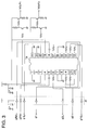
- Fig. 3 is a circuit diagram showing an example of the CCD and its peripheral circuit.
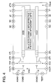
- Fig. 4 is a circuit diagram showing an example of the CCD line sensor.
- Fig. 5 is a time chart showing an example of the operation of the CCD.
- Fig. 6 is a diagram showing the correlation between the drive frequency of the CCD and the temperature.
- Fig. 7 is a diagram showing the correlation between the peripheral temperature of the CCD and the dark current.
- Fig. 8 is a time chart showing a change in the temperature inside the apparatus when the fan is operated.
- Fig. 1 is a block diagram for showing the circuit of the example of the image reading apparatus to which the present invention is applied.
- the circuit shown in this block diagram is assembled to the reading section of a digital type copier.
- a document is exposed to a beam of light.
- the beam of light having image information is received by the CCD line sensor 1 illustrated in Fig. 1.
- the image on the document is read out by the action of photoelectric conversion.
- the first and second oscillators 2, 3 are provided, the oscillating frequencies of which are different.
- the first oscillator 2 generates clock pulses, the frequency of which is appropriate for the predetermined reading operation conducted by the CCD sensor 1.
- the second oscillator 3 generates clock pulses, the frequency of which lower than that of the first oscillator 2.
- the clock pulses generated by the first and second oscillators 2, 3 are respectively inputted into the switching circuit 4. Then the switching circuit 4 selectively outputs one of the clock pulses in accordance with the clock designation signal CTRL sent from the reading control circuit 6 having the CPU 5.
- the clock pulse outputted from the switching circuit 4 is inputted into the CCD drive pulse generation circuit 7 which is a drive pulse signal generating means.
- the CCD drive pulse generation circuit 7 a drive pulse signal for driving the CCD line sensor 1 is generated in accordance with the inputted clock pulse.
- the clock pulse to be inputted into the CCD drive pulse generation circuit 7 is changed over by the switching circuit 4 and the image reading control circuit 6. Therefore, the switching circuit 4 and the image reading control circuit 6 correspond to the drive speed switching means in this example.
- the drive pulse signal generated by the CCD drive pulse generation circuit 7 is given to the CCD driver circuit 8.
- the transfer clock pulses ⁇ 1, ⁇ 2, shift signal ⁇ SH , and reset signal ⁇ RS are formed in accordance with the aforementioned drive pulse signal, and these pulse signals are impressed upon the CCD line sensor 1, so that the CCD line sensor 1 can be operated.
- the CCD sensor includes a package la of the CCD line sensor, and various peripheral circuits.
- the construction of the sensor package la is shown in Fig. 4.
- the sensor package la is operated by a timed relation shown in the time chart of Fig. 5 in accordance with the pulse signals of the transfer clock pulses ⁇ 1, ⁇ 2, shift signal ⁇ SH , and reset signal ⁇ RS . Then the output OS of the CCD line sensor 1 is sent to the analog signal processing circuit 9.
- the analog signal processing circuit 9 converts an analog signal sent from the CCD line sensor 1 into a digital signal. This digital signal is outputted to an image processing section (not shown) together with the pixel clock signal CLK and the horizontal synchronization signal H ⁇ V.
- the digital image signal is subjected to various image processing such as magnification processing, reduction processing and spatial frequency processing.
- image processing for example, a laser beam is modulated, and the modulated laser beam is irradiated on the photoreceptor drum, so that an electrostatic latent image id formed on the surface of the photoreceptor drum.
- the electrostatic latent image is developed with toner, and then the developed toner image is transferred and fixed on a recording sheet. In this way, the document is copied.
- the vertical synchronization signal V ⁇ V is outputted from the reading control circuit 6.
- the movement of the optical reading system is controlled in the subsidiary scanning direction.
- a dark current in the CCD which is a solid state image pickup element used for the CCD line sensor 1
- the dark current can be the cause of image deterioration. Therefore, it is necessary to suppress the increase in the environmental temperature.
- the substantial reading time is short. Accordingly, when the generation of heat in the period of waiting for the next reading operation is suppressed, the increase in the environmental temperature (the temperature inside the apparatus) can be avoided.
- a normal clock pulse of the first oscillator 2 is selected during the period of reading operation, and a clock pulse of relatively low frequency of the second oscillator 3 is selected during the period of waiting for the next reading operation.
- a drive pulse signal of relatively high frequency is generated in the period of reading, the CCD is driven at high speed so that reading can be carried out in the predetermined manner.
- a pulse signal of frequency lower than that of the period of reading is generated, so that the CCD is driven at low speed.
- the drive frequency is lowered as compared with that of the reading operation. Due to the foregoing, the generation of heat of the CCD and its peripheral circuits can be suppressed in the waiting condition. Further, when the generation of heat is appropriately permitted, a large difference of temperature is not caused between the waiting and reading conditions.
- the generation of heat from the CCD and its peripheral circuits is suppressed during a long period of waiting for the next reading operation. Due to the foregoing, the necessity of forcible ventilation conducted by a fan can be reduced. When the necessity of forcible ventilation conducted by a fan is reduced, the possibility of deterioration of image quality caused by dust can be decreased. When the CCD is driven at low speed even in the case of waiting, the sudden drop of CCD temperature can be avoided. As a result of the foregoing, the CCD temperature can be stabilized, so that the CCD output characteristics can be made constant.
- the oscillating clock pulse of the second oscillator 2 is used for controlling the heat generation in the period of waiting for the next reading operation as described above. Accordingly, the oscillating clock pulse of the second oscillator 2 may be appropriately determined so that the temperature rise can be prevented, while consideration is given to the characteristics of the CCD to be used and the environment by which the apparatus is surrounded.
- the solid state image pickup element can be driven at a lower speed in the waiting period than that in the reading operation period. Due to the foregoing, the generation of heat by the solid state image pickup element and its peripheral circuit can be suppressed in the period of waiting for the next reading operation, so that the temperature rise in the apparatus can be avoided. Further, the solid state image pickup element is driven at low speed in the waiting period so that the generation of heat can be appropriately conducted for stabilizing the temperature of the solid state image pickup element. Consequently, while the necessity of radiation conducted by the fan is lowered, the temperature of the solid state image pickup element can be stabilized. As a result, the output characteristics of the solid state image pickup element can be maintained in a good condition, and the quality of images can be improved when they are read.
Landscapes
- Engineering & Computer Science (AREA)
- Multimedia (AREA)
- Signal Processing (AREA)
- Physics & Mathematics (AREA)
- Electromagnetism (AREA)
- Facsimile Heads (AREA)
- Facsimile Scanning Arrangements (AREA)
Applications Claiming Priority (2)
| Application Number | Priority Date | Filing Date | Title |
|---|---|---|---|
| JP5049281A JPH06268821A (ja) | 1993-03-10 | 1993-03-10 | 画像読取り装置 |
| JP49281/93 | 1993-03-10 |
Publications (2)
| Publication Number | Publication Date |
|---|---|
| EP0615376A2 true EP0615376A2 (de) | 1994-09-14 |
| EP0615376A3 EP0615376A3 (de) | 1994-10-12 |
Family
ID=12826494
Family Applications (1)
| Application Number | Title | Priority Date | Filing Date |
|---|---|---|---|
| EP19940301585 Withdrawn EP0615376A3 (de) | 1993-03-10 | 1994-03-07 | Bildlesegerät. |
Country Status (2)
| Country | Link |
|---|---|
| EP (1) | EP0615376A3 (de) |
| JP (1) | JPH06268821A (de) |
Cited By (5)
| Publication number | Priority date | Publication date | Assignee | Title |
|---|---|---|---|---|
| EP0792065A3 (de) * | 1996-02-26 | 1999-05-26 | Canon Kabushiki Kaisha | Photoelektrische Umwandlungsvorrichtung und Methode zur Ansteuerung der Vorrichtung |
| US6127684A (en) * | 1996-02-26 | 2000-10-03 | Canon Kabushiki Kaisha | Photoelectric conversion apparatus and driving method of the apparatus |
| US6448561B1 (en) | 1996-02-26 | 2002-09-10 | Canon Kabushiki Kaisha | Photoelectric conversion apparatus and driving method of the apparatus |
| US7372494B2 (en) | 2003-03-28 | 2008-05-13 | Fujilfilm Corporation | Solid-state image pickup apparatus driven at a frequency adaptive to photographic sensitivity |
| US7710485B2 (en) | 2006-03-14 | 2010-05-04 | Fujifilm Corporation | Solid-state image pickup apparatus with signal charge transfer adaptive to an image shooting condition |
Families Citing this family (1)
| Publication number | Priority date | Publication date | Assignee | Title |
|---|---|---|---|---|
| JP5081865B2 (ja) * | 2009-05-22 | 2012-11-28 | 京セラドキュメントソリューションズ株式会社 | 画像読取装置及び画像形成装置 |
Family Cites Families (5)
| Publication number | Priority date | Publication date | Assignee | Title |
|---|---|---|---|---|
| JPS6450670A (en) * | 1987-08-20 | 1989-02-27 | Canon Kk | Picture processor |
| JPH01192259A (ja) * | 1988-01-28 | 1989-08-02 | Canon Inc | フイルム画像読取装置 |
| JP2891475B2 (ja) * | 1989-04-14 | 1999-05-17 | 三菱電機株式会社 | 電荷転送素子の駆動回路 |
| JPH0377470A (ja) * | 1989-08-21 | 1991-04-03 | Ricoh Co Ltd | 画像読取装置 |
| JP3029444B2 (ja) * | 1990-06-21 | 2000-04-04 | 株式会社リコー | 画像読取装置 |
-
1993
- 1993-03-10 JP JP5049281A patent/JPH06268821A/ja active Pending
-
1994
- 1994-03-07 EP EP19940301585 patent/EP0615376A3/de not_active Withdrawn
Cited By (6)
| Publication number | Priority date | Publication date | Assignee | Title |
|---|---|---|---|---|
| EP0792065A3 (de) * | 1996-02-26 | 1999-05-26 | Canon Kabushiki Kaisha | Photoelektrische Umwandlungsvorrichtung und Methode zur Ansteuerung der Vorrichtung |
| US6127684A (en) * | 1996-02-26 | 2000-10-03 | Canon Kabushiki Kaisha | Photoelectric conversion apparatus and driving method of the apparatus |
| US6448561B1 (en) | 1996-02-26 | 2002-09-10 | Canon Kabushiki Kaisha | Photoelectric conversion apparatus and driving method of the apparatus |
| US7372494B2 (en) | 2003-03-28 | 2008-05-13 | Fujilfilm Corporation | Solid-state image pickup apparatus driven at a frequency adaptive to photographic sensitivity |
| US7944494B2 (en) | 2003-03-28 | 2011-05-17 | Fujifilm Corporation | Solid-state image pickup apparatus driven at a frequency adaptive to photographic sensitivity |
| US7710485B2 (en) | 2006-03-14 | 2010-05-04 | Fujifilm Corporation | Solid-state image pickup apparatus with signal charge transfer adaptive to an image shooting condition |
Also Published As
| Publication number | Publication date |
|---|---|
| EP0615376A3 (de) | 1994-10-12 |
| JPH06268821A (ja) | 1994-09-22 |
Similar Documents
| Publication | Publication Date | Title |
|---|---|---|
| KR920000570B1 (ko) | 영상형성장치 및 반도체레이저의 출력제어방법 | |
| US5412408A (en) | Beam recording apparatus with intensity control | |
| JP3155538B2 (ja) | レーザの多階調書き込み装置 | |
| JPH06268821A (ja) | 画像読取り装置 | |
| US5812174A (en) | Device for driving a laser diode and an electrophotography type image forming apparatus using the same | |
| US5481371A (en) | Image reading device having variable internal synronization setting control | |
| US6204865B1 (en) | Color image forming apparatus timing control | |
| US6195108B1 (en) | Image formation method for forming electrostatic latent image on photosensitive belt with laser beam and image formation apparatus of the same | |
| JPH04353878A (ja) | 画像形成装置 | |
| JPH0349364A (ja) | 画像形成装置 | |
| JP2872271B2 (ja) | 画像形成装置 | |
| US6836279B2 (en) | Light beam scanning apparatus and image forming apparatus | |
| US5450118A (en) | Image forming apparatus | |
| US20030169464A1 (en) | Image reading apparatus | |
| US20060187979A1 (en) | Laser control circuit and image forming apparatus | |
| JP3630766B2 (ja) | 画像形成装置及びその制御方法 | |
| JP4367840B2 (ja) | 画素クロック生成装置、光走査装置及び画像形成装置 | |
| JPH1026849A (ja) | 画像形成装置及びその方法 | |
| JPH05330129A (ja) | 画像形成装置 | |
| JP2003195580A (ja) | 画像形成装置および画像形成方法 | |
| JP3160310B2 (ja) | 画像形成装置と画像形成方法 | |
| JPH07266612A (ja) | 画像形成装置 | |
| JPH04289880A (ja) | 露光装置 | |
| JPH02112379A (ja) | 画像処理装置 | |
| JPH0266584A (ja) | 像形成装置 |
Legal Events
| Date | Code | Title | Description |
|---|---|---|---|
| PUAI | Public reference made under article 153(3) epc to a published international application that has entered the european phase |
Free format text: ORIGINAL CODE: 0009012 |
|
| PUAL | Search report despatched |
Free format text: ORIGINAL CODE: 0009013 |
|
| AK | Designated contracting states |
Kind code of ref document: A2 Designated state(s): DE FR GB IT NL |
|
| AK | Designated contracting states |
Kind code of ref document: A3 Designated state(s): DE FR GB IT NL |
|
| 17P | Request for examination filed |
Effective date: 19950218 |
|
| 17Q | First examination report despatched |
Effective date: 19970211 |
|
| GRAG | Despatch of communication of intention to grant |
Free format text: ORIGINAL CODE: EPIDOS AGRA |
|
| STAA | Information on the status of an ep patent application or granted ep patent |
Free format text: STATUS: THE APPLICATION HAS BEEN WITHDRAWN |
|
| 18W | Application withdrawn |
Withdrawal date: 19980309 |