EP0617410B1 - Procédé de fabrication d'une tête magnétique à minces film et tête magnétique obtenable au moyen de ce procédé - Google Patents
Procédé de fabrication d'une tête magnétique à minces film et tête magnétique obtenable au moyen de ce procédé Download PDFInfo
- Publication number
- EP0617410B1 EP0617410B1 EP19940200677 EP94200677A EP0617410B1 EP 0617410 B1 EP0617410 B1 EP 0617410B1 EP 19940200677 EP19940200677 EP 19940200677 EP 94200677 A EP94200677 A EP 94200677A EP 0617410 B1 EP0617410 B1 EP 0617410B1
- Authority
- EP
- European Patent Office
- Prior art keywords
- layer
- magnetic
- soft
- flux
- insulation layer
- Prior art date
- Legal status (The legal status is an assumption and is not a legal conclusion. Google has not performed a legal analysis and makes no representation as to the accuracy of the status listed.)
- Expired - Lifetime
Links
- 238000000034 method Methods 0.000 title claims description 75
- 239000010409 thin film Substances 0.000 title claims description 13
- 238000004519 manufacturing process Methods 0.000 title claims description 10
- 238000009413 insulation Methods 0.000 claims description 65
- 238000005498 polishing Methods 0.000 claims description 61
- VYPSYNLAJGMNEJ-UHFFFAOYSA-N silicon dioxide Inorganic materials O=[Si]=O VYPSYNLAJGMNEJ-UHFFFAOYSA-N 0.000 claims description 54
- 239000000696 magnetic material Substances 0.000 claims description 43
- 239000000463 material Substances 0.000 claims description 42
- 239000002585 base Substances 0.000 claims description 34
- MCMNRKCIXSYSNV-UHFFFAOYSA-N Zirconium dioxide Chemical compound O=[Zr]=O MCMNRKCIXSYSNV-UHFFFAOYSA-N 0.000 claims description 28
- 239000000758 substrate Substances 0.000 claims description 28
- 229910045601 alloy Inorganic materials 0.000 claims description 24
- 239000000956 alloy Substances 0.000 claims description 24
- 229910000859 α-Fe Inorganic materials 0.000 claims description 22
- 229910052681 coesite Inorganic materials 0.000 claims description 18
- 229910052906 cristobalite Inorganic materials 0.000 claims description 18
- 239000010453 quartz Substances 0.000 claims description 18
- 239000000377 silicon dioxide Substances 0.000 claims description 18
- 229910052682 stishovite Inorganic materials 0.000 claims description 18
- 229910052905 tridymite Inorganic materials 0.000 claims description 18
- 239000000243 solution Substances 0.000 claims description 17
- 238000011282 treatment Methods 0.000 claims description 16
- 125000006850 spacer group Chemical group 0.000 claims description 13
- 239000002245 particle Substances 0.000 claims description 11
- 229910001030 Iron–nickel alloy Inorganic materials 0.000 claims description 10
- 239000003795 chemical substances by application Substances 0.000 claims description 10
- 238000005530 etching Methods 0.000 claims description 10
- 239000010432 diamond Substances 0.000 claims description 6
- 229910003460 diamond Inorganic materials 0.000 claims description 6
- 230000001939 inductive effect Effects 0.000 claims description 6
- 239000000725 suspension Substances 0.000 claims description 5
- 239000003513 alkali Substances 0.000 claims description 4
- 238000000151 deposition Methods 0.000 claims description 4
- 239000012777 electrically insulating material Substances 0.000 claims description 4
- 230000002463 transducing effect Effects 0.000 claims description 4
- 239000012670 alkaline solution Substances 0.000 claims 1
- 239000010410 layer Substances 0.000 description 162
- HEMHJVSKTPXQMS-UHFFFAOYSA-M Sodium hydroxide Chemical compound [OH-].[Na+] HEMHJVSKTPXQMS-UHFFFAOYSA-M 0.000 description 12
- 230000004907 flux Effects 0.000 description 12
- 230000008901 benefit Effects 0.000 description 10
- 238000004804 winding Methods 0.000 description 10
- 238000004544 sputter deposition Methods 0.000 description 9
- 239000012792 core layer Substances 0.000 description 7
- 238000007517 polishing process Methods 0.000 description 7
- 235000019589 hardness Nutrition 0.000 description 6
- 229920002120 photoresistant polymer Polymers 0.000 description 6
- 230000007547 defect Effects 0.000 description 4
- 238000011049 filling Methods 0.000 description 4
- 238000000992 sputter etching Methods 0.000 description 4
- 239000000126 substance Substances 0.000 description 4
- 229910003962 NiZn Inorganic materials 0.000 description 3
- PNEYBMLMFCGWSK-UHFFFAOYSA-N aluminium oxide Inorganic materials [O-2].[O-2].[O-2].[Al+3].[Al+3] PNEYBMLMFCGWSK-UHFFFAOYSA-N 0.000 description 3
- 229910052593 corundum Inorganic materials 0.000 description 3
- 230000000694 effects Effects 0.000 description 3
- 229910001845 yogo sapphire Inorganic materials 0.000 description 3
- CSCPPACGZOOCGX-UHFFFAOYSA-N Acetone Chemical compound CC(C)=O CSCPPACGZOOCGX-UHFFFAOYSA-N 0.000 description 2
- 239000012790 adhesive layer Substances 0.000 description 2
- 230000007797 corrosion Effects 0.000 description 2
- 238000005260 corrosion Methods 0.000 description 2
- 230000008878 coupling Effects 0.000 description 2
- 238000010168 coupling process Methods 0.000 description 2
- 238000005859 coupling reaction Methods 0.000 description 2
- 230000008021 deposition Effects 0.000 description 2
- 238000010438 heat treatment Methods 0.000 description 2
- 230000005415 magnetization Effects 0.000 description 2
- 239000002105 nanoparticle Substances 0.000 description 2
- 230000008569 process Effects 0.000 description 2
- 238000003631 wet chemical etching Methods 0.000 description 2
- 229910002971 CaTiO3 Inorganic materials 0.000 description 1
- 239000000853 adhesive Substances 0.000 description 1
- 230000001070 adhesive effect Effects 0.000 description 1
- 229910002113 barium titanate Inorganic materials 0.000 description 1
- 230000015572 biosynthetic process Effects 0.000 description 1
- 239000013590 bulk material Substances 0.000 description 1
- 239000011248 coating agent Substances 0.000 description 1
- 238000000576 coating method Methods 0.000 description 1
- 239000004020 conductor Substances 0.000 description 1
- 239000000470 constituent Substances 0.000 description 1
- 238000001816 cooling Methods 0.000 description 1
- 239000002178 crystalline material Substances 0.000 description 1
- 238000010292 electrical insulation Methods 0.000 description 1
- 238000002474 experimental method Methods 0.000 description 1
- 230000002349 favourable effect Effects 0.000 description 1
- 239000011521 glass Substances 0.000 description 1
- 238000000227 grinding Methods 0.000 description 1
- 238000009499 grossing Methods 0.000 description 1
- JEIPFZHSYJVQDO-UHFFFAOYSA-N iron(III) oxide Inorganic materials O=[Fe]O[Fe]=O JEIPFZHSYJVQDO-UHFFFAOYSA-N 0.000 description 1
- 238000000608 laser ablation Methods 0.000 description 1
- 231100001231 less toxic Toxicity 0.000 description 1
- 239000007788 liquid Substances 0.000 description 1
- 238000005259 measurement Methods 0.000 description 1
- 230000006911 nucleation Effects 0.000 description 1
- 238000010899 nucleation Methods 0.000 description 1
- 229910000889 permalloy Inorganic materials 0.000 description 1
- 238000001020 plasma etching Methods 0.000 description 1
- 230000001681 protective effect Effects 0.000 description 1
- 239000011241 protective layer Substances 0.000 description 1
- 230000035945 sensitivity Effects 0.000 description 1
- 238000004528 spin coating Methods 0.000 description 1
- 229910052566 spinel group Inorganic materials 0.000 description 1
- 239000012086 standard solution Substances 0.000 description 1
- 230000003746 surface roughness Effects 0.000 description 1
- 238000012360 testing method Methods 0.000 description 1
- 238000012546 transfer Methods 0.000 description 1
- XLYOFNOQVPJJNP-UHFFFAOYSA-N water Substances O XLYOFNOQVPJJNP-UHFFFAOYSA-N 0.000 description 1
Images


Classifications
-
- G—PHYSICS
- G11—INFORMATION STORAGE
- G11B—INFORMATION STORAGE BASED ON RELATIVE MOVEMENT BETWEEN RECORD CARRIER AND TRANSDUCER
- G11B5/00—Recording by magnetisation or demagnetisation of a record carrier; Reproducing by magnetic means; Record carriers therefor
- G11B5/127—Structure or manufacture of heads, e.g. inductive
- G11B5/33—Structure or manufacture of flux-sensitive heads, i.e. for reproduction only; Combination of such heads with means for recording or erasing only
- G11B5/39—Structure or manufacture of flux-sensitive heads, i.e. for reproduction only; Combination of such heads with means for recording or erasing only using magneto-resistive devices or effects
- G11B5/3903—Structure or manufacture of flux-sensitive heads, i.e. for reproduction only; Combination of such heads with means for recording or erasing only using magneto-resistive devices or effects using magnetic thin film layers or their effects, the films being part of integrated structures
- G11B5/3906—Details related to the use of magnetic thin film layers or to their effects
- G11B5/3916—Arrangements in which the active read-out elements are coupled to the magnetic flux of the track by at least one magnetic thin film flux guide
- G11B5/3919—Arrangements in which the active read-out elements are coupled to the magnetic flux of the track by at least one magnetic thin film flux guide the guide being interposed in the flux path
- G11B5/3922—Arrangements in which the active read-out elements are coupled to the magnetic flux of the track by at least one magnetic thin film flux guide the guide being interposed in the flux path the read-out elements being disposed in magnetic shunt relative to at least two parts of the flux guide structure
- G11B5/3925—Arrangements in which the active read-out elements are coupled to the magnetic flux of the track by at least one magnetic thin film flux guide the guide being interposed in the flux path the read-out elements being disposed in magnetic shunt relative to at least two parts of the flux guide structure the two parts being thin films
Definitions
- the invention relates to a method of manufacturing a thin-film magnetic head comprising a magnetoresistive element and at least one flux-guiding element, which method starts from a support.
- the magnetic heads obtained by means of the methods described in EP-A 0 516 022 are integrated magnetic heads having a contact face and comprising an inductive part and a magnetoresistive part.
- a first structured insulation layer of SiO 2 is formed on a magnetic substrate of a ferrite by means of a lithographic method, which layer is subsequently provided with a layer of Au for forming a write coil.
- a second structured insulation layer is provided on which a core layer of an amorphous material based on Co is deposited. This core layer is in contact with the magnetic substrate via apertures in the insulation layers.
- the parts of the second insulation layer not coated by the core layer are filled up by means of a filling layer of Al 2 O 3 . After the filling layer has been formed. the core layer and the filling layer are planed by means of lapping.
- a third structured insulation layer of SiO 2 is deposited on the surface thus obtained on which subsequently a bias winding of Au is formed.
- a fourth structured insulation layer of SiO 2 is provided on this winding.
- a magnetoresistive element of permalloy is formed on this insulation layer.
- a fifth structured insulation layer of SiO 2 is provided and subsequently a yoke of an amorphous material which is based on Co and is in contact with the core layer via apertures in the three last-mentioned insulation layers.
- two flux guides of a Co-based amorphous material are provided on a non-magnetic substrate, while an aperture between the two flux guides is filled with a first insulation layer of SiO 2 .
- the surface formed by the flux guides and the first insulation layer is provided with a second structured insulation layer on which subsequently a magnetoresistive (MR) element is formed.
- the MR element is then coated with a third structured insulation layer on which subsequently a bias winding is formed.
- a fourth structured insulation layer is provided for the purpose of coating the bias winding.
- a magnetic core layer of a Co-based material is formed which is in contact with one of the flux guides via apertures in the three last-mentioned insulation layers.
- the areas not coated by the first core layer are filled up with a filling layer of Al 2 O 3 , whereafter a surface on which an inductive head part is formed is obtained by lapping.
- the MR element is formed on an insulation layer which is provided on a lapping-processed surface.
- a surface extending on two or more adjacent layers of different material has unevenness.
- damage particularly in the form of scratches in and disturbances of material under the surface obtained are caused by lapping.
- Such a surface is inadmissible, inefficient for information transfer and may increase the risk of instabilities in the MR element provided on said surface.
- the magnetic heads obtained by the methods known from EP-A 0 516 022 have the further drawback that due to the presence of irregularities on the surface engaging the MR element, a relatively thick insulation layer is required between the MR element and the electrically conducting flux guides so as to ensure a reliable electrical insulation between the MR element and the flux guides.
- insulation layers have a further negative influence on the efficiency of the magnetic heads. For various reasons, damage in and material disturbance under a surface above which the MR element is present are thus undesirable.
- JP-A 63 3179915 discloses a yoke type thin film magnetic head having a front yoke and a back yoke formed on a substrate by a bulk material.
- a thin film MR element is arranged between the yokes in an electrically insulated but magnetically coupled way.
- the method according to the invention starts from a support having a support face on which a first insulation layer of a non-magnetic material is formed, on which insulation layer a soft-magnetic layer having an upper face remote from the first insulation layer is formed by depositing a soft-magnetic material and is characterized in that after forming of the soft-magnetic layer, a layer portion is removed for forming the flux-guiding element, whereafter non-magnetic material is deposited on a remaining portion of the soft-magnetic layer and on a free portion of the first insulation layer for forming a second insulation layer having an upper face remote from the soft-magnetic layer, said second insulation layer having such a thickness that, viewed in a direction transverse to the support face, the smallest distance between the support face and the upper face of the second insulation layer is larger than the largest distance between the support face and the upper face of the soft-magnetic layer, whereafter a mechanochemical polishing treatment is performed as from the upper face of the second insulation layer for forming a main surface
- a very plane and smooth main surface which is free from damage is obtained for providing the magnetoresistive element (MR element) in an electrically insulated manner, which results in a magnetic head having a stable MR element and an efficiency which is improved with respect to that of the known magnetic heads.
- MR element magnetoresistive element
- mechanochemical polishing is performed with the aid of a working surface of a polishing tool which is urged against and moved across the surface to be polished.
- the working surface is provided with a liquid mechanochemical polishing agent. This is an agent with which chemical and mechanical polishing is simultaneously possible.
- polishing without damage can be realised by purely chemical polishing.
- This method has drawbacks.
- the geometrical control, i.e. the planeness of the surface is far from optimal and many chemical polishing agents are more or less toxic and aggressive and should consequently be used in an extremely protected environment, which is a drawback in mass production.
- the mechanochemical polishing operation in which components mechanically removed from the surface to be polished are chemically dissolved, leads to a very smooth and plane polished surface which is free from damage.
- An embodiment of the method according to the invention is characterized in that the mechanochemical polishing treatment is performed down to the soft-magnetic layer.
- the mechanochemical polishing treatment is performed on non-magnetic material as well as on soft-magnetic material. It has surprisingly been found that despite the consequently different material properties mechanochemically polishing yields a very plane and smooth main surface without the materials themselves undergoing any structural changes. It has also been found that if one of the materials to be polished is very hard, the mechanical aspect of mechanochemically polishing will be enhanced by adding a small quantity of hard, adequate grains to the polishing agent of the mechanochemical type. Thus, even when using combinations of materials of divergent mechanical hardnesses, smooth and plane surfaces which are free from damage can be realised in the manufacture of magnetic heads.
- An embodiment of the method according to the invention is characterized in that a spacer layer of a non-magnetic, electrically insulating material, on which the magnetoresistive material is deposited, is formed on the main surface obtained by means of mechanochemical polishing.
- the spacer layer may be formed from known materials such as quartz or zirconia which can be provided in a well-defined manner by means of known techniques.
- This method according to the invention is particularly important if use is made of electrically conducting soft-magnetic materials for forming the flux-guiding elements. In that case an insulating spacer layer is necessary in order to prevent electrical contact between the flux-guiding elements and the MR element.
- a drawback of a magnetic head having a spacer layer between the MR element and the flux-guiding elements is, however, that due to the distance between the MR element and the flux-guiding elements caused by the thickness of the spacer layer only a portion of the magnetic flux originating during operation from a magnetic recording medium is passed through the MR element. For reasons of efficiency it is therefore of essential importance that such a layer can be made as thin as possible.
- this spacer layer may be perfectly smooth and have no thickness variations when the method according to the invention is used, and, moreover, it may be very thin, for example 0.2 ⁇ m with respect to the layer thicknesses of at least 0.6 ⁇ m required in the known magnetic heads, without any risk of short-circuit of the MR element.
- An embodiment of the method according to the invention is characterized in that the second insulation layer is mechanochemically polished up to a predetermined distance to the upper face of the soft-magnetic layer, whereafter the magnetoresistive material is deposited on the main surface obtained.
- This embodiment has the advantage that only one type of material is to be polished mechanochemically.
- the use of one type of material and consequently mechanochemically polishing one material has the great advantage that both the thickness of the layer to be deposited, and the rate of removal during mechanochemical polishing can be determined accurately. Both factors ensure reliable geometrical control of the desired layer thickness.
- the second insulation layer of the given thickness is planarized. If the second insulation layer is planarized, it is either possible to stop in this insulation layer at a desired level or to continue polishing down to the soft-magnetic layer. It is recommended to take hardness differences between the non-magnetic material and the soft-magnetic material into account from the start of the mechanochemical polishing process.
- An embodiment of the method according to the invention is characterized in that a plate-shaped substrate is used which is provided with two parallel substrate faces by means of mechanical and/or mechanochemical polishing, whereafter one of these faces is used as a support face. The other face is used as a reference face in the further process steps.
- the parallel substrate faces may be obtained by starting from a substrate having two substrate faces, the substrate faces being first prepared by means of polishing until they have a convex, plane or concave initial shape, whereafter a removal cycle is run through at least once, during which the substrate faces of a substrate whose edges are thicker than a central piece surrounded by the edges are polished in such a way that the edges successively acquire a substantially equal thickness, a smaller thickness and again a substantially equal thickness as the central piece, and during which cycle the substrate faces of a substrate whose edges are thinner than a central piece surrounded by the edges are polished in such a way that the edges successively acquire a substantially equal thickness, a larger thickness and again a substantially equal thickness as the central piece.
- the above-mentioned method of manufacturing parallel faces is described extensively in European Patent Application 92201739.7 (PHN 14.081 EP-P; herewith incorporated by reference).
- Substrates having parallel substrate faces have the great advantage that they can be used in a mass manufacturing process for the further steps of the method. Consequently, mechanochemical polishing steps can be performed at a later stage for the purpose of smoothing and planing a layer having a single or multiple material structure and for stop-polishing a layer having a multiple material structure, but of which only one or some materials of the layer can be polished via the mechanochemical polishing process and the other material cannot be polished.
- An embodiment of the method is characterized in that the substrate is formed from a soft-magnetic material, particularly a ferrite.
- a ferrite is understood to be a magnetic material of, for example one of the following crystallographic groups: garnets, spinels, perovskites. Favourable properties of ferrite are its great wear resistance and its satisfactory shielding effect against disturbing fields. The stability of a magnetoresistive head is usually also favourably influenced by the effect of the ferrite on the thin-film flux-guiding elements and the magnetoresistive element. Moreover, a ferrite substrate has the technological advantage that the substrate can be used as a flux-guiding layer.
- An embodiment is characterized in that a base element is used on which an inductive transducing element, a base layer of a non-magnetic material and a flux-guiding layer are provided, whereafter a mechanochemical polishing treatment is performed for forming the support face.
- the base layer may be provided with a recess by removing material from a side remote from the base element, preferably by means of etching, which recess is subsequently filled up with a soft-magnetic material for forming the flux-guiding layer.
- This method yields a magnetic head having a write function as well as a read function. During the method a write portion and subsequently a read portion is formed.
- the base layer is also mechanochemically polished in this embodiment.
- a magnetical advantage on making a planar write portion cannot be achieved. However, a maximum planeness is necessary to obtain a planar read portion having the previously mentioned advantages.
- An embodiment is characterized in that the base element is plate-shaped and is provided with two parallel base faces by means of mechanical and/or mechanochemical polishing, whereafter the base layer is formed on one of said faces.
- the parallel base faces may be obtained by means of the method described in European Patent Application no. 92201739.7. Also in this case elements with parallel faces have advantages as far as mass manufacture, mechanochemical polishing of single materials and mechanochemical polishing of distributed materials are concerned.
- An embodiment is characterized in that the base element is formed from a soft-magnetic material, particularly a ferrite.
- An embodiment is characterized in that the main layer is formed from quartz. Quartz may be provided, for example by means of PE-CVD. It has been found that if the mechanochemical polishing treatment is performed down to the soft-magnetic material, the soft-magnetic material of the flux-guiding elements will hardly have any influence on the eminent result of the mechanochemical polishing process, notably in so far as the surface is plane and free from damage.
- the main layer is formed from zirconia.
- Zirconia is a crystalline material in a cubic form.
- the main constituent is ZrO 2 to which 5-10 at.% of CaO or Y 2 O 3 are added.
- Zirconia which may be provided, for example by sputtering, is a mechanically hard and wear-resistant material. Probably due to its great hardness, zirconia, together with all soft-magnetic materials to be further described, forms a substantially perfect main surface after mechanochemical polishing.
- zirconia and the much softer quartz can be subjected to similar polishing treatments when the mechanochemical polishing process is optimized.
- quartz has technological advantages because it can be easily deposited and etched.
- zirconia has the advantage that it is much more wear-resistant.
- An embodiment is characterized in that an alloy from the group of alloys formed by CoZrNb alloys, FeNbSi alloys, FeSiAl alloys and NiFe alloys is used as a soft-magnetic material. These materials may be provided by means of known techniques such as sputtering or vapour deposition. In the present invention the soft-magnetic material is etched for forming the flux-guiding element. NiFe and FeNbSi alloys can relatively easily be etched wet-chemically. For CoZrNb and FeSiAl alloys sputter-etching or reactive ion etching is preferably used.
- An embodiment is characterized in that a ferrite is used as a soft-magnetic material.
- a ferrite usually has such a high resistivity that the MR element can be directly provided on the flux-guiding elements formed from such a material without resulting in any noticeable loss of sensitivity of the magnetic head.
- the spacer layer may be omitted in the method according to the invention and a layer of a magnetoresistive material may thus be directly provided on the main surface for forming the MR element. Consequently, a direct magnetic coupling between the MR element and the flux-guiding elements is possible. Such a coupling results in a high efficiency of the magnetic head obtained.
- Ferrites can be provided by means of known techniques such as sputtering, MO-CVD or laser ablation.
- the magnetic head obtained by means of the method according to the invention is provided with a head face for cooperation with a magnetic recording medium, particularly a magnetic tape or disc, while a flux-guiding element terminates in the head face.
- ferrite flux- guiding elements have the advantage that the ferrite contributes to the corrosion resistance and the wear resistance of the head face.
- An embodiment is characterized in that an NiFe alloy is used as a magnetoresistive material.
- the NiFe alloy can be provided by means of known techniques such as sputter-deposition or vapour deposition.
- the MR element formed from NiFe is provided with contact faces for realising an electrical connection with a read device.
- equipotential strips having a satisfactory electrical conductivity are provided on the NiFe layer formed so as to linearize the behaviour of the MR element. This measure is described in US 4,052,748 (herewith incorporated by reference).
- An embodiment is characterized in that the base layer is formed from quartz.
- An embodiment is characterized in that the base layer is formed from zirconia.
- An embodiment is characterized in that the recess in the base layer is provided by means of etching.
- An embodiment is characterized in that the mechanochemical polishing treatment is performed with a colloidal suspension of SiO 2 particles in an alkali solution, particularly a KOH or NaOH solution.
- a colloidal suspension of SiO 2 nano particles may be used for this purpose, having, for example an average grain size of 30 nm.
- the NaOH or KOH solution may have a pH of approximately 10.
- mechanochemical polishing is known per se from IBM Technical Disclosure Bulletin, vol 27, no. 8, January 1985. This publication describes mechanochemical polishing of a glass structure. It is also known per se to use an agent commercially available under the trade name Syton for the mechanochemical polishing process.
- An embodiment is characterized in that the mechanochemical polishing treatment is performed with a mechanochemical polishing agent comprising a colloidal SiO 2 solution in which grains are present which have an average particle size of less than 1.0 micrometer and a hardness which is better than the hardness of SiO 2 .
- a mechanochemical polishing agent comprising a colloidal SiO 2 solution in which grains are present which have an average particle size of less than 1.0 micrometer and a hardness which is better than the hardness of SiO 2 .
- This method according to the invention yields a very smooth mechanochemically polished main surface. It has been found that a surface roughness R(rms) of the polished surface smaller than 1 nm can be achieved. Measurements have shown that there is no damage or defect of the material structure of the mechanochemically polished surface. The above also applies to mechanochemical polishing of the substrate and the base layer.
- Al 2 O 3 or zirconia is suitable as a material for the grains, but diamond is preferred because the materials are to be polished.
- a colloidal SiO 2 solution provided with diamond grains having an average particle size of less than 1.0 ⁇ m is therefore preferred as a polishing agent.
- the invention also relates to a thin-film magnetic head obtained by means of the method according to the invention and having a head face for cooperation with a magnetic recording medium, in which the flux-guiding element terminates in the head face.
- the magnetoresistive element has a very plane, accurately defined base, so that the magnetical stability of the magnetoresistive element is ensured. Due to the applied method according to the invention, corrosion-resistant and/or wear-resistant materials may be used for layers terminating in the head face, so that a long lifetime of the head face, hence of the complete magnetic head, is possible.
- the invention also relates to a thin-film magnetic head obtainable by means of the method according to the invention and having a head face in which a flux-guiding element terminates, which magnetic head is characterized in that a further flux-guiding element spaced apart from said flux-guiding element is provided, a spacing between the two flux-guiding elements being bridged by a magnetoresistive element located opposite a mechanochemically polished second insulation layer.
- the presence of two flux-guiding elements guarantees a high efficiency.
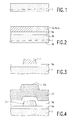
- a first embodiment of the invention will be described with reference to Figs. 1 to 17.
- This method starts from a plate-shaped substrate 1 of ferrite, an NiZn ferrite in this embodiment, which is provided with two parallel substrate faces 3a and 3b by means of polishing. Polishing may be effected by means of known polishing methods, but the method described in European Patent Application no. 92201739.7 is preferably used.
- An insulation layer 5a of quartz is formed, for example by means of PE-CVD, on one of the substrate faces, in this embodiment the substrate face 3a serving as a support.
- an adhesive layer 7a of MO, a layer 7b of Au and an adhesive layer 7c of Mo are successively deposited on the layer 5a by means of, for example sputter-deposition for forming a test and/or bias winding 7.
- a photoresist layer is provided by means of, for example spin coating on the joint layers 7a, 7b, 7c. This layer is dried and subsequently exposed, using a suitable photomask. Subsequently the exposed photoresist is developed and then removed by rinsing in water.
- the layer 7c of Mo is etched whereafter the unexposed photoresist is removed by means of acetone and the layer 7b of Au is processed by means of sputter-etching with an Mo pattern as a mask.
- the winding 7 is obtained by subsequent etching of the Mo layer 7c.
- An insulation layer 5b of quartz is provided by means of, for example PE-CVD on the layer 5a and the winding 7 on this layer.
- the layers 5a and 5b jointly constitute a first insulation layer 5 of a non-magnetic material.
- a soft-magnetic layer 17 having an upper face 17c remote from the first insulation layer 5 is formed, for example, by means of sputter-deposition of an FeNbSi alloy on the first insulation layer 5 provided on the substrate 1 functioning as a support, which insulation layer functions as a read gap. By heating FeNbSi after sputtering in a magnetic field, a layer is obtained which is both magnetically soft and mechanically hard and wear-resistant.
- a layer 9 of Mo is provided, for example by means of sputter-deposition on the soft-magnetic layer 17, whereafter Mo is removed by means of etching in the areas 11a and 11b for structuring the layer 9. Subsequently the soft-magnetic layer 17 is sputter-etched, with the structured layer 9 functioning as a mask and with the two layer portions 17a and 17b being left. After sputter-etching, the parts of the layer 9 possibly left are removed, for example by wet-chemical etching.
- a second insulation layer 18 having an upper face remote from the layer portions 17a and 17b is formed from quartz by means of, for example PE-CVD on the remaining portions 17a and 17b of the soft-magnetic layer 17 and on an interpositioned, bared portion 5c of the first insulation layer 5.
- Material is deposited until the second insulation layer 18 has a thickness at which the smallest distance d s between the upper face 18a and the support face 3a is larger than the largest distance d l between the upper face 17c and the support face 3a.
- the second insulation layer 18 thus formed is mechanochemically polished for forming a substantially perfectly plane and smooth main surface 19 which is free from defects.
- the mechanochemical polishing treatment is initially performed on a small polishing surface. After some polishing, the polishing surface increases.
- the layer thickness of the second insulation layer 18 is chosen to be such, and the mechanochemical polishing process is adapted to be such that a plane and smooth surface p is already formed before the soft-magnetic material of the portions 17a and 17b is reached by mechanochemical polishing. This ensures that the main surface 19, which is partly formed by the non-magnetic material of the second insulation layer 18 and partly by the soft-magnetic material of the layer portions 17a and 17b, is plane, smooth and free from defects despite differences in hardness between the non-magnetic material and the soft-magnetic material.
- the mechanochemical polishing treatment which is also referred to as tribo-chemical polishing in literature, is performed with a colloidal suspension of SiO 2 particles in an alkali solution, for example NaOH to which diamond grains having an average size of less than 1.0 ⁇ m are added.
- concentration of the diamond grains in said solution is less than 1 g per litre.
- a thin spacer layer 21 of a non-magnetic, electrically insulating material is provided on the plane, defectless main surface 19 obtained in the manner described above.
- quartz is deposited by means of PE-CVD for this purpose.
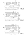
- a layer 23a of a magnetoresistive material is provided on the spacer layer 21, for which purpose an alloy of NiFe is sputtered in this embodiment.
- the layer 23a is subsequently structured by means of a photoresist mask and etching to form an MR element 23.
- a layer 25a of an electrically conducting material, for example Au is provided on the MR element 23, which layer is structured by means of a photoresist mask and etching to form equipotential strips 25 of a barberpole structure and to form electrically conducting strips 25b for electrically connecting the MR element to a measuring device (not shown).
- an insulation layer 27 of, for example quartz is provided by means of, for example PE-CVD.
- Apertures 29 extending as far as the conducting strips 25b are etched in this insulation layer in order to provide electrical connections, whereafter a protective counterblock 31 of, for example BaTiO 3 or CaTiO 3 is secured by means of, for example an adhesive.
- the layer 27 may be planed to a desired thickness in advance, for example by mechanical polishing or lapping.
- the unit now obtained is provided with a head face 33 for cooperation with a magnetic recording medium, particularly a magnetic tape by means of operations such as grinding and/or lapping.
- the MR element 23 may be directly provided on the main surface 19. Consequently, the insulation layer 21 may be dispensed with and the MR element 23 may be in direct magnetical contact with the flux-guiding elements 17A and 17B.
- the formed polished surface p shown in Fig. 9 as a main surface. In that case it is not necessary to provide a spacer layer 21 as is shown in Fig. 11.
- the desired insulation is ensured by the non-magnetic, electrically insulating material present between the soft-magnetic portions 17a and 17b used as flux guides and the polished surface p.
- the predetermined distance d of the polished surface p up to the upper face 17c can be achieved with great accuracy.
- the mechanochemical polishing treatment can be carried out with a colloidal suspension of SiO 2 particles in an alkali solution, for example, a standard solution commercially available under the trade name Syton .
- zirconia may be used instead of quartz, while the insulation layers are preferably formed by means of sputtering.
- FIG. 18 A second embodiment of the method according to the invention will be described with reference to Figs. 18 to 29.
- This method starts from a plate-shaped base element 101, preferably of ferrite which is polished on both sides for forming two parallel base faces 102a and 102b.
- An insulation layer 104a of quartz is provided by means of, for example PE-CVD on one of the base faces, in this embodiment the face 102b.
- An electrically conducting layer 106a of, for example mainly Au is provided on the layer 104a.
- This layer 106a is structured by means of known techniques to form an inductive transducing element or winding 106.
- quartz is deposited for forming an insulation layer 104b and an aperture 108 is etched in the two insulation layers 104a and 104b.
- a relatively thick insulation layer 104c of quartz is provided.
- the layers 104a, 104b and 104c jointly constitute a base layer 104 of a non-magnetic material.
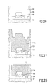
- a layer 110 of a mask material, for example Mo is provided on the base layer 104 provided on the base element 101, with which mask material layer an aperture 112 is formed in the base layer 104.
- a photoresist is first deposited and structured on the layer 110, whereafter apertures 112 are formed in the layer 110 by means of etching for forming a mask.
- the base layer 104 is sputter-etched with the structured layer 110 as a mask for forming the aperture 102.
- a layer 114a of a soft-magnetic material for example a CoZrNb alloy is provided on the base layer 104 thus structured, while the aperture 102 is completely filled up.
- the layer 114a is used for forming a flux-guiding element 114.
- the base layer 104 provided with the filled aperture 102 is subsequently mechanochemically polished by means of a polishing agent comprising an alkaline colloidal SiO 2 solution to which diamond particles are added for creating a plane support face 116 which is free from scratches.
- a first insulation layer 105 of a non-magnetic material is formed on the base face 116 thus obtained.
- Flux-guiding elements 117A and 117B are provided in the main layer 105 in a manner analogous to that described with reference to the first embodiment of the method according to the invention.
- a main surface 119 is also formed by means of mechanochemical polishing, whereafter an MR element 123 is provided.
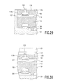
- a thin-film magnetic head manufactured by means of the second embodiment of the method according to the invention is shown in Fig. 30.
- the magnetic head has a head face 118 and comprises a base element 101 on which a non-magnetic base layer 104 is provided.
- the base layer 104 accommodates a winding 106 serving as an inductive transducing element and a flux guide 114 of a soft-magnetic material terminating in the head face 118.
- a non-magnetic main layer 105 consisting of a first and a second insulation layer and accommodating a front flux guide 117A terminating in the head face 118 and a rear flux guide 117B is provided on a mechanochemically polished support face 116.
- Both flux guides or flux-guiding elements are formed from a soft-magnetic material.
- a bias winding 107 may extend in the layer 105.
- the layer 105 has a mechanochemically polished main surface 119 on which - with a thin electrically insulating spacer layer being interpositioned - an MR element 123 is provided directly or indirectly.
- the invention is of course not limited to the embodiments shown.
Landscapes
- Engineering & Computer Science (AREA)
- Manufacturing & Machinery (AREA)
- Magnetic Heads (AREA)
Claims (25)
- Procédé de fabrication d'une tête magnétique à couche mince comprenant un élément magnétorésistif (23, 123) et au moins un élément de guidage de flux (17A, 17B ; 117A, 117B), lequel procédé part d'un support ayant une face de support (116) sur laquelle est formée une première couche isolante (5, 105) d'un matériau non magnétique, couche isolante sur laquelle une couche magnétique douce (17) ayant une face supérieure (17c) distante de la première couche isolante est formée par dépôt d'un matériau magnétique doux, caractérisé en ce que, après la formation de la couche magnétique douce (17), une partie de couche est retirée pour former l'élément de guidage de flux (17A, 17B ; 117A, 117B), après quoi un matériau non magnétique est déposé sur une partie restante (17a, 17b) de la couche magnétique douce et sur une partie libre de la première couche isolante pour former une seconde couche isolante (18) ayant une face supérieure (18a) distante de la couche magnétique douce, ladite seconde couche isolante ayant une épaisseur à laquelle, observée dans une direction transversale à la face de support, la plus petite distance (ds) entre la face de support et la face supérieure de la seconde couche isolante est supérieure à la plus grande distance (d1) entre la face de support (17c) et la face supérieure de la couche magnétique douce, après quoi un traitement de polissage mécanochimique est réalisé à partir de la face supérieure de la seconde couche isolante pour former une surface principale (19, 119) sur laquelle un matériau magnétorésistif est ensuite déposé pour former l'élément magnétorésistif (23, 123).
- Procédé selon la revendication 1, caractérisé en ce que le traitement de polissage mécanochimique est réalisé jusqu'à la couche magnétique douce (17).
- Procédé selon la revendication 2, caractérisé en ce qu'une couche d'écartement (21) en un matériau électriquement isolant non magnétique, sur laquelle est déposé le matériau magnétorésistif, est formé sur la surface principale (19) obtenue par polissage mécanochimique.
- Procédé selon la revendication 1, caractérisé en ce que la seconde couche isolante (18) est polie mécanochimiquement jusqu'à une distance prédéterminée de la face supérieure (17c) de la couche magnétique douce (17), après quoi le matériau magnétorésistif est déposé sur la surface principale (19) obtenue.
- Procédé selon la revendication 1, 2, 3 ou 4, caractérisé en ce que l'on utilise un substrat en forme de plaque (1) qui est muni de deux faces de substrat parallèles (3a, 3b) au moyen d'un polissage mécanique et/ou mécanochimique, après quoi l'une desdites faces est utilisée comme face de support.
- Procédé selon la revendication 5, caractérisé en ce que le substrat (1 ) est formé d'un matériau magnétique doux.
- Procédé selon la revendication 1, 2, 3 ou 4, caractérisé en ce que l'on utilise un élément de base (101) sur lequel sont disposés un élément transducteur inductif (106), une couche de base (104) en un matériau non magnétique et une couche de guidage de flux (114a), après quoi un traitement de polissage mécanochimique est réalisé pour former la face de support (116).
- Procédé selon la revendication 7, caractérisé en ce que l'élément de base (101) est en forme de plaque et est muni de deux faces de base parallèles (102a, 102b) au moyen d'un polissage mécanique et/ou mécanochimique, après quoi la couche de base (104) est formée sur l'une desdites faces.
- Procédé selon la revendication 7 ou 8, caractérisé en ce que l'élément de base (101) est formé d'un matériau magnétique doux.
- Procédé selon l'une quelconque des revendications précédentes, caractérisé en ce que le quartz est utilisé comme matériau non magnétique.
- Procédé selon l'une quelconque des revendications 1 à 9 précédentes, caractérisé en ce que la zircone est utilisée comme matériau non magnétique.
- Procédé selon l'une quelconque des revendications précédentes, caractérisé en ce que la partie de couche de la couche magnétique douce (17) est retirée par attaque.
- Procédé selon l'une quelconque des revendications précédentes, caractérisé en ce qu'un alliage du groupe d'alliages constitué par les alliages CoZrNb, les alliages FeNbSi, les alliages FeSiAl et les alliages NiFe est utilisé comme matériau magnétique doux.
- Procédé selon l'une quelconque des revendications 1 à 12, caractérisé en ce qu'un ferrite est utilisé comme matériau magnétique doux.
- Procédé selon l'une quelconque des revendications précédentes, caractérisé en ce qu'un alliage NiFe est utilisé comme matériau magnétorésistif.
- Procédé selon la revendication 7, 8 ou 9, caractérisé en ce que la couche de base (104) est formée de quartz.
- Procédé selon la revendication 7, 8 ou 9, caractérisé en ce que la couche de base (104) et formée de zircone.
- Procédé selon la revendication 7, 8, 9, 16 ou 17, caractérisé en ce qu'un évidement (112) dans la couche de base (104) est formé par attaque, lequel évidement est ensuite rempli d'un matériau magnétique doux pour former la couche de guidage de flux (114a).
- Procédé selon l'une quelconque des revendications précédentes, caractérisé en ce que le traitement de polissage mécanochimique est réalisé avec une suspension colloïdale de particules de SiO2 dans une solution alcaline.
- Procédé selon l'une quelconque des revendications 1 à 18, caractérisé en ce que le traitement de polissage mécanochimique est réalisé avec un agent de polissage mécanochimique comprenant une solution de SiO2 colloïdale dans laquelle des grains sont présents.
- Procédé selon la revendication 20, caractérisé en ce qu'une solution alcaline est utilisée comme solution de SiO2.
- Procédé selon la revendication 20 ou 21, caractérisé en ce que l'on utilise des grains qui ont une taille moyenne de particules inférieure à 1,0 µm et une dureté qui est meilleure que la dureté de SiO2.
- Procédé selon la revendication 20, 21 ou 22, caractérisé en ce que l'on utilise des grains de diamant.
- Procédé selon la revendication 20, 21, 22 ou 23, caractérisé en ce qu'une concentration de grains inférieure à 1 g/l est utilisée dans la solution colloïdale.
- Tête magnétique à couche mince obtenue par le procédé selon l'une quelconque des revendications 1 à 24 et ayant une face de tête (118) dans laquelle aboutit un élément de guidage de flux (117A), un autre élément de guidage de flux (117B) distant dudit élément de guidage de flux est formé, un espace entre les deux éléments de guidage de flux (117A) étant franchi par un élément magnétorésistif (123) situé en position opposée à une seconde couche isolante polie mécanochimiquement.
Priority Applications (1)
| Application Number | Priority Date | Filing Date | Title |
|---|---|---|---|
| EP19940200677 EP0617410B1 (fr) | 1993-03-22 | 1994-03-16 | Procédé de fabrication d'une tête magnétique à minces film et tête magnétique obtenable au moyen de ce procédé |
Applications Claiming Priority (5)
| Application Number | Priority Date | Filing Date | Title |
|---|---|---|---|
| BE9300274 | 1993-03-22 | ||
| BE9300274A BE1006925A3 (nl) | 1993-03-22 | 1993-03-22 | Werkwijze voor het vervaardigen van een dunnefilm magneetkop en magneetkop vervaardigd volgens de werkwijze. |
| EP93200993 | 1993-04-06 | ||
| EP93200993 | 1993-04-06 | ||
| EP19940200677 EP0617410B1 (fr) | 1993-03-22 | 1994-03-16 | Procédé de fabrication d'une tête magnétique à minces film et tête magnétique obtenable au moyen de ce procédé |
Publications (3)
| Publication Number | Publication Date |
|---|---|
| EP0617410A2 EP0617410A2 (fr) | 1994-09-28 |
| EP0617410A3 EP0617410A3 (fr) | 1996-12-11 |
| EP0617410B1 true EP0617410B1 (fr) | 1999-09-22 |
Family
ID=27159798
Family Applications (1)
| Application Number | Title | Priority Date | Filing Date |
|---|---|---|---|
| EP19940200677 Expired - Lifetime EP0617410B1 (fr) | 1993-03-22 | 1994-03-16 | Procédé de fabrication d'une tête magnétique à minces film et tête magnétique obtenable au moyen de ce procédé |
Country Status (1)
| Country | Link |
|---|---|
| EP (1) | EP0617410B1 (fr) |
Families Citing this family (3)
| Publication number | Priority date | Publication date | Assignee | Title |
|---|---|---|---|---|
| US5767673A (en) * | 1995-09-14 | 1998-06-16 | Lucent Technologies Inc. | Article comprising a manganite magnetoresistive element and magnetically soft material |
| TW369649B (en) * | 1997-02-20 | 1999-09-11 | Koninkl Philips Electronics Nv | Single-channel magnetoresistive magnetic head and device including such a magnetic head |
| US5890278A (en) * | 1997-04-01 | 1999-04-06 | U.S. Philips Corporation | Method of manufacturing a magnetic head having a structure of layers |
Family Cites Families (7)
| Publication number | Priority date | Publication date | Assignee | Title |
|---|---|---|---|---|
| JPS59152521A (ja) * | 1983-02-21 | 1984-08-31 | Hitachi Ltd | 磁気抵抗効果型多素子磁気ヘツド |
| JPS60177420A (ja) * | 1984-02-23 | 1985-09-11 | Nec Corp | 複合型薄膜磁気ヘツド及びその製造方法 |
| JPS6292219A (ja) * | 1985-10-18 | 1987-04-27 | Victor Co Of Japan Ltd | 磁気抵抗効果型薄膜磁気ヘツド |
| JP2505465B2 (ja) * | 1987-06-19 | 1996-06-12 | 関西日本電気株式会社 | ヨ−ク型薄膜磁気ヘッド |
| JPH01289224A (ja) * | 1988-05-17 | 1989-11-21 | Sumitomo Special Metals Co Ltd | 薄膜磁気ヘッド用基板及びその製造方法 |
| JPH02154309A (ja) * | 1988-12-07 | 1990-06-13 | Tdk Corp | 薄膜磁気ヘッド用基板の製造方法 |
| EP0519558B1 (fr) * | 1991-06-18 | 1996-09-18 | Koninklijke Philips Electronics N.V. | Tête de lecture/écriture à couche mince sans effet de recouvrement |
-
1994
- 1994-03-16 EP EP19940200677 patent/EP0617410B1/fr not_active Expired - Lifetime
Also Published As
| Publication number | Publication date |
|---|---|
| EP0617410A2 (fr) | 1994-09-28 |
| EP0617410A3 (fr) | 1996-12-11 |
Similar Documents
| Publication | Publication Date | Title |
|---|---|---|
| EP0617409B1 (fr) | Procédé de fabrication d'une tête magnétique à film minces et tête magnétique obtenable au moyen de ce procédé | |
| US5483735A (en) | Method of manufacturing a thin-film magnetic head | |
| EP0584707B1 (fr) | Aggloméré stratifié et dispositif de lecture à couche mince résistant à l'usure formé sur un tel aggloméré | |
| EP0634465B1 (fr) | Méthode de polissage d'une surface en cuivre ou en alliage à majorité de cuivre | |
| US7207100B2 (en) | Method of manufacturing a magnetic head | |
| US7181827B2 (en) | Method of forming magnetic layer pattern | |
| US6580586B1 (en) | Magnetic transducer with recessed magnetic elements | |
| US6673633B2 (en) | Method of forming patterned thin film and method of manufacturing thin-film magnetic head | |
| JPH04252407A (ja) | 磁気書込/読取ヘッドの製造方法 | |
| EP0617410B1 (fr) | Procédé de fabrication d'une tête magnétique à minces film et tête magnétique obtenable au moyen de ce procédé | |
| US6631550B2 (en) | Method of manufacturing a thin-film magnetic head | |
| HK1013363B (en) | Method of manufacturing a thin-film magnetic head, and magnetic head obtainable by means of said method | |
| US5815910A (en) | Method for manufacturing a magnetic head | |
| HK1013720B (en) | Method of manufacturing a thin-film magnetic head, and magnetic head obtainable by means of said method | |
| BE1006925A3 (nl) | Werkwijze voor het vervaardigen van een dunnefilm magneetkop en magneetkop vervaardigd volgens de werkwijze. | |
| EP1053565A1 (fr) | Procede de formation d'un ensemble de couches empilees | |
| US6183891B1 (en) | Magnetic head and method of manufacture | |
| US20030219980A1 (en) | Pattern forming method, method of making microdevice, method of making thin-film magnetic head, method of making magnetic head slider, method of making magnetic head apparatus, and method of making magnetic recording and reproducing apparatus | |
| KR100363235B1 (ko) | 자기헤드의제조방법 | |
| JPH11241160A (ja) | 絶縁膜の成膜方法及び薄膜磁気ヘッドの製造方法 | |
| JP2001176026A (ja) | ヨーク型スピンバルブ磁気ヘッド及びその製造方法 | |
| JPH10302221A (ja) | 磁気ヘッドの製造方法 | |
| US20020057525A1 (en) | Method of manufacturing a magnetic element | |
| EP1034534A1 (fr) | Procede de fabrication d'une tete magnetique comportant une couche mince | |
| JPH11273031A (ja) | 磁気抵抗効果型磁気ヘッド |
Legal Events
| Date | Code | Title | Description |
|---|---|---|---|
| PUAI | Public reference made under article 153(3) epc to a published international application that has entered the european phase |
Free format text: ORIGINAL CODE: 0009012 |
|
| AK | Designated contracting states |
Kind code of ref document: A2 Designated state(s): DE ES FR GB |
|
| RAP1 | Party data changed (applicant data changed or rights of an application transferred) |
Owner name: N.V. PHILIPS' GLOEILAMPENFABRIEKEN |
|
| PUAL | Search report despatched |
Free format text: ORIGINAL CODE: 0009013 |
|
| RAP1 | Party data changed (applicant data changed or rights of an application transferred) |
Owner name: PHILIPS ELECTRONICS N.V. |
|
| AK | Designated contracting states |
Kind code of ref document: A3 Designated state(s): DE ES FR GB |
|
| 17P | Request for examination filed |
Effective date: 19970611 |
|
| 17Q | First examination report despatched |
Effective date: 19971208 |
|
| GRAG | Despatch of communication of intention to grant |
Free format text: ORIGINAL CODE: EPIDOS AGRA |
|
| RAP3 | Party data changed (applicant data changed or rights of an application transferred) |
Owner name: KONINKLIJKE PHILIPS ELECTRONICS N.V. |
|
| GRAG | Despatch of communication of intention to grant |
Free format text: ORIGINAL CODE: EPIDOS AGRA |
|
| GRAH | Despatch of communication of intention to grant a patent |
Free format text: ORIGINAL CODE: EPIDOS IGRA |
|
| GRAH | Despatch of communication of intention to grant a patent |
Free format text: ORIGINAL CODE: EPIDOS IGRA |
|
| GRAA | (expected) grant |
Free format text: ORIGINAL CODE: 0009210 |
|
| RAP1 | Party data changed (applicant data changed or rights of an application transferred) |
Owner name: ONSTREAM, INC. |
|
| AK | Designated contracting states |
Kind code of ref document: B1 Designated state(s): DE ES FR GB |
|
| REF | Corresponds to: |
Ref document number: 69420766 Country of ref document: DE Date of ref document: 19991028 |
|
| ET | Fr: translation filed | ||
| REG | Reference to a national code |
Ref country code: ES Ref legal event code: FG2A Ref document number: 2139044 Country of ref document: ES Kind code of ref document: T3 |
|
| PLBE | No opposition filed within time limit |
Free format text: ORIGINAL CODE: 0009261 |
|
| STAA | Information on the status of an ep patent application or granted ep patent |
Free format text: STATUS: NO OPPOSITION FILED WITHIN TIME LIMIT |
|
| 26N | No opposition filed | ||
| REG | Reference to a national code |
Ref country code: GB Ref legal event code: IF02 |
|
| PGFP | Annual fee paid to national office [announced via postgrant information from national office to epo] |
Ref country code: ES Payment date: 20020311 Year of fee payment: 9 |
|
| PG25 | Lapsed in a contracting state [announced via postgrant information from national office to epo] |
Ref country code: ES Free format text: LAPSE BECAUSE OF NON-PAYMENT OF DUE FEES Effective date: 20030317 |
|
| PGFP | Annual fee paid to national office [announced via postgrant information from national office to epo] |
Ref country code: FR Payment date: 20030331 Year of fee payment: 10 Ref country code: DE Payment date: 20030331 Year of fee payment: 10 |
|
| PGFP | Annual fee paid to national office [announced via postgrant information from national office to epo] |
Ref country code: GB Payment date: 20030404 Year of fee payment: 10 |
|
| PG25 | Lapsed in a contracting state [announced via postgrant information from national office to epo] |
Ref country code: GB Free format text: LAPSE BECAUSE OF NON-PAYMENT OF DUE FEES Effective date: 20040316 |
|
| REG | Reference to a national code |
Ref country code: ES Ref legal event code: FD2A Effective date: 20030317 |
|
| PG25 | Lapsed in a contracting state [announced via postgrant information from national office to epo] |
Ref country code: DE Free format text: LAPSE BECAUSE OF NON-PAYMENT OF DUE FEES Effective date: 20041001 |
|
| GBPC | Gb: european patent ceased through non-payment of renewal fee |
Effective date: 20040316 |
|
| PG25 | Lapsed in a contracting state [announced via postgrant information from national office to epo] |
Ref country code: FR Free format text: LAPSE BECAUSE OF NON-PAYMENT OF DUE FEES Effective date: 20041130 |
|
| REG | Reference to a national code |
Ref country code: FR Ref legal event code: ST |