EP0618083A1 - Plaque de circuit integre - Google Patents
Plaque de circuit integre Download PDFInfo
- Publication number
- EP0618083A1 EP0618083A1 EP93916231A EP93916231A EP0618083A1 EP 0618083 A1 EP0618083 A1 EP 0618083A1 EP 93916231 A EP93916231 A EP 93916231A EP 93916231 A EP93916231 A EP 93916231A EP 0618083 A1 EP0618083 A1 EP 0618083A1
- Authority
- EP
- European Patent Office
- Prior art keywords
- card
- module
- substrate
- end portion
- long side
- Prior art date
- Legal status (The legal status is an assumption and is not a legal conclusion. Google has not performed a legal analysis and makes no representation as to the accuracy of the status listed.)
- Granted
Links
Images



Classifications
-
- G—PHYSICS
- G06—COMPUTING OR CALCULATING; COUNTING
- G06K—GRAPHICAL DATA READING; PRESENTATION OF DATA; RECORD CARRIERS; HANDLING RECORD CARRIERS
- G06K19/00—Record carriers for use with machines and with at least a part designed to carry digital markings
- G06K19/06—Record carriers for use with machines and with at least a part designed to carry digital markings characterised by the kind of the digital marking, e.g. shape, nature, code
- G06K19/067—Record carriers with conductive marks, printed circuits or semiconductor circuit elements, e.g. credit or identity cards also with resonating or responding marks without active components
- G06K19/07—Record carriers with conductive marks, printed circuits or semiconductor circuit elements, e.g. credit or identity cards also with resonating or responding marks without active components with integrated circuit chips
- G06K19/077—Constructional details, e.g. mounting of circuits in the carrier
- G06K19/0772—Physical layout of the record carrier
- G06K19/07728—Physical layout of the record carrier the record carrier comprising means for protection against impact or bending, e.g. protective shells or stress-absorbing layers around the integrated circuit
-
- G—PHYSICS
- G06—COMPUTING OR CALCULATING; COUNTING
- G06K—GRAPHICAL DATA READING; PRESENTATION OF DATA; RECORD CARRIERS; HANDLING RECORD CARRIERS
- G06K19/00—Record carriers for use with machines and with at least a part designed to carry digital markings
- G06K19/04—Record carriers for use with machines and with at least a part designed to carry digital markings characterised by the shape
-
- G—PHYSICS
- G06—COMPUTING OR CALCULATING; COUNTING
- G06K—GRAPHICAL DATA READING; PRESENTATION OF DATA; RECORD CARRIERS; HANDLING RECORD CARRIERS
- G06K19/00—Record carriers for use with machines and with at least a part designed to carry digital markings
- G06K19/06—Record carriers for use with machines and with at least a part designed to carry digital markings characterised by the kind of the digital marking, e.g. shape, nature, code
- G06K19/067—Record carriers with conductive marks, printed circuits or semiconductor circuit elements, e.g. credit or identity cards also with resonating or responding marks without active components
- G06K19/07—Record carriers with conductive marks, printed circuits or semiconductor circuit elements, e.g. credit or identity cards also with resonating or responding marks without active components with integrated circuit chips
- G06K19/077—Constructional details, e.g. mounting of circuits in the carrier
- G06K19/07745—Mounting details of integrated circuit chips
-
- G—PHYSICS
- G06—COMPUTING OR CALCULATING; COUNTING
- G06K—GRAPHICAL DATA READING; PRESENTATION OF DATA; RECORD CARRIERS; HANDLING RECORD CARRIERS
- G06K19/00—Record carriers for use with machines and with at least a part designed to carry digital markings
- G06K19/06—Record carriers for use with machines and with at least a part designed to carry digital markings characterised by the kind of the digital marking, e.g. shape, nature, code
- G06K19/08—Record carriers for use with machines and with at least a part designed to carry digital markings characterised by the kind of the digital marking, e.g. shape, nature, code using markings of different kinds or more than one marking of the same kind in the same record carrier, e.g. one marking being sensed by optical and the other by magnetic means
-
- G—PHYSICS
- G06—COMPUTING OR CALCULATING; COUNTING
- G06K—GRAPHICAL DATA READING; PRESENTATION OF DATA; RECORD CARRIERS; HANDLING RECORD CARRIERS
- G06K19/00—Record carriers for use with machines and with at least a part designed to carry digital markings
- G06K19/06—Record carriers for use with machines and with at least a part designed to carry digital markings characterised by the kind of the digital marking, e.g. shape, nature, code
- G06K19/08—Record carriers for use with machines and with at least a part designed to carry digital markings characterised by the kind of the digital marking, e.g. shape, nature, code using markings of different kinds or more than one marking of the same kind in the same record carrier, e.g. one marking being sensed by optical and the other by magnetic means
- G06K19/083—Constructional details
-
- H—ELECTRICITY
- H10—SEMICONDUCTOR DEVICES; ELECTRIC SOLID-STATE DEVICES NOT OTHERWISE PROVIDED FOR
- H10W—GENERIC PACKAGES, INTERCONNECTIONS, CONNECTORS OR OTHER CONSTRUCTIONAL DETAILS OF DEVICES COVERED BY CLASS H10
- H10W90/00—Package configurations
- H10W90/701—Package configurations characterised by the relative positions of pads or connectors relative to package parts
- H10W90/751—Package configurations characterised by the relative positions of pads or connectors relative to package parts of bond wires
- H10W90/754—Package configurations characterised by the relative positions of pads or connectors relative to package parts of bond wires between a chip and a stacked insulating package substrate, interposer or RDL
Definitions
- the present invention relates to an IC card with a built-in semiconductor integrated circuit device, particularly to a structure of an IC card having a front surface on which ready access terminals are provided for connecting to an external device and a reverse surface on which a magnetic body line (magnetic stripe) is provided for storing information therein.
- a magnetic body line magnetic stripe
- An IC card comprises a central processing unit (CPU) and a memory circuit which are respectively built in a card. That is, the IC card is a kind of computer. Accordingly, the IC card can be applied to a variety of purposes.
- CPU central processing unit
- memory circuit which are respectively built in a card. That is, the IC card is a kind of computer. Accordingly, the IC card can be applied to a variety of purposes.
- the standardization of the IC card is now under progress internationally according to a standard of an International Organization for Standardization (hereinafter refereed to as an ISO) and in Japan according to a standard of a Japanese Industrial Standard (hereinafter referred to as a JIS).
- ISO International Organization for Standardization
- JIS Japanese Industrial Standard
- a distance A ranging from an upper end 101 of an IC card 100 to an upper side of ready access terminals 103-1, 103-2 (a side nearest to the upper end 101 among sides defining terminals) of an IC chip module 103 is set to be 19.23 mm in maximum as illustrated in Fig. 15.
- a distance B ranging from the upper end 101 of the IC card 100 to a base of a third track 105a of a magnetic stripe 105 is prescribed to be 15.32 mm at minimum and 15.82 mm at maximum as illustrated in Fig. 16.
- Fig. 17 is an enlarged cross-sectional view of a main portion of the IC card provided with a magnetic stripe which meets the standard as set forth above (which is a so-called JIS-I type IC card in Japan).
- a positional relation between the IC chip module 103 and the magnetic stripe 105 can be easily understood from Fig. 17.
- a distance C ranging from the upper end 101 of the IC card to a base of the magnetic stripe 105 comes to 16.82 mm which is the sum of the distance B ranging from the upper end 101 to the base of the third track 105a, i.e. 15.82 mm in maximum and a 1 mm margin for covering errors. Since the distance A ranging from the upper end 101 to the upper sides of the ready access terminals 103-1, 103-2 is 19.23 mm in maximum, a distance D ranging from the upper end 101 to the upper side of the IC chip module 103 comes to 18.23 mm which is the difference between the distance A and a 1 mm margin to be involved in manufacturing the module.
- An IC card comprises a card substrate having front and reverse surfaces, a magnetic stripe formed on the reverse surface for storing information therein and a module which is formed on a given region of the front surface and includes a semiconductor integrated circuit device therein provided with ready access terminals for connecting with an external device, wherein an end portion of the module is positioned perpendicular to the magnetic stripe.
- An IC card according to a second aspect of the invention is structured in that the thickness of the end portion of the module is gradually thinned.
- An IC card according to a third aspect of the invention is structured in that a part of the end portion of the module is point-shaped. More in detail, the module is formed pentagonal or hexagonal and is arranged in a manner that a tip end of the end portion of the module is point-shaped.
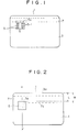
- Fig. 1 is a plan view showing an external appearance of an IC card according to a first embodiment of the present invention
- Fig. 2 is a plan view of the IC card according to the first embodiment of the present invention
- Fig. 3 is a cross-sectional view of a main portion of the IC card of Fig. 2
- Fig. 4 is an enlarged cross-sectional view explaining in detail the cross-sectional view of the main portion of Fig. 3
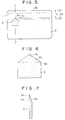
- Fig. 5 is a plan view of an IC card according to a second embodiment of the present invention
- Fig. 6 is a plan view of an IC chip module according to the second embodiment
- Fig. 7 is a cross-sectional view of the IC chip module of Fig. 6, Fig.
- FIG. 8 is a cross-sectional view of a main portion of the IC card for explaining the positional relation between the IC chip module and a magnetic stripe according to the second embodiment
- Fig. 9 is an enlarged cross-sectional view for explaining in detail the cross-sectional view of the main portion of Fig. 8
- Fig. 10 is a plan view of an IC card according to a third embodiment of the present invention
- Fig. 11 is a plan view of an IC chip module according the a third embodiment
- Fig. 12 is a cross-sectional view of the IC chip module of Fig. 11, Fig.
- FIG. 13 is a cross-sectional view of a main portion of the IC card for explaining the positional relation between the IC chip module and a magnetic stripe according to the third embodiment
- Fig. 14 is an enlarged cross-sectional view for explaining in detail the cross-sectional view of the main portion of Fig. 13
- Fig. 15 is a plan view showing an external appearance of a front surface of a general IC card
- Fig. 16 is a plan view showing an external appearance of a reverse surface of the IC card of Fig.
- Fig. 17 is a cross-sectional view of a main portion of the IC card of Fig. 15
- Fig. 18 is a cross-sectional view for explaining the state where stress is applied to the IC card of Fig. 15.
- Fig. 1 is a plan view of an IC card according to the present embodiment. This plan view is typically illustrated for explaining the present invention.
- An IC card 1 which is the same as a general IC card in that it comprises an IC chip module 5 (hereinafter referred to as a module) which is provided on the front surface of an IC card substrate 3 and includes a semiconductor circuit device therein provided with a plurality of read access terminals 5-1 for connecting to an external device and a magnetic stripe 7 which is provided on a reverse surface of the card substrate 3 for storing information therein.
- a feature of the present invention resides in that an end 5a of the module 5 (denoted at one dotted chain line in Fig. 1) is positioned to extend to an upper portion of the magnetic stripe 7 provided on the reverse surface of the card substrate 3.
- Fig. 2 schematically shows the IC card of Fig. 1.
- FIG. 3 A cross-sectional view of a main portion of the IC card as taken along X-X' of Fig. 2 is illustrated in Fig. 3 so that the positional relation between the module 5 and the magnetic stripe 7 is easily understood.
- the IC card of the present embodiment has the module end portion of which is positioned to extend to the upper portion of the magnetic stripe 7. That is, as mentioned above, the module 5 is disposed so that the distance L is less than the distance M.
- the module 5 comprises a substrate 5-2, a semiconductor circuit device 5-3 mounted on one surface of the substrate 5-2, a mold resin 5-4 for covering the substrate 5-2 and the semiconductor circuit device 5-3 and ready access terminals 5-1 provided on the other surface of the substrate 5-2 so as to connect to an external device (not shown).
- the module is generally accommodated in a module accommodation portion which is a so-called spot facing defined on the front surface of the card substrate and its neighboring portion.
- the magnetic stripe 7 is also accommodated in the so-called spot facing defined on the reverse surface of the card substrate and its neighboring portion.
- the structure per se of the module of the present invention is the same as that of the general IC card, the overall structure of the module is different from that of the general IC card in that the end portion 5a of the module of the present invention is positioned to extend to the upper portion of the magnetic stripe and this is the feature of the present invention.
- FIG. 5 A second embodiment of the present invention will be described with reference to Figs. 5 to 9.
- components which are the same as those explained in the first embodiment are denoted at the same numerals and explanation thereof is omitted.
- Fig. 5 is a plan view of an IC card typically illustrating the present embodiment.
- the IC card in this embodiment has a point-shaped portion 5b which is formed as illustrated in Fig. 6 at the end portion 5a of the module 5 of the IC card in the first embodiment and the thickness of the end portion 5b is gradually thinned toward a tip end 5c as illustrated in Fig. 7.
- the module is pentagonal in plane and the thickness of the module 5 is gradually thinned from a base 5d of the end portion 5b toward the tip end 5c. That is, the end portion 5b has a tapered portion 5e.
- a distance N ranging from the upper end 3a of the IC card substrate 3 to the upper end, i. e., tip end 5c of the module 5 is formed to be less than a distance M ranging from the upper end 3a to a base 7a of the magnetic stripe 7.
- FIG. 8 A cross-sectional view of the main portion taken along Y-Y' of Fig. 5 is illustrated in Fig. 8 so that the positional relation between the module 5 and the magnetic stripe 7 is easily understood.
- the IC card of the present embodiment has the module 5 end portion of which is positioned to extend to the upper portion of the magnetic stripe 7 and the thickness of the end portion is gradually thinned.
- FIG. 9 A portion which enlarges and describes the module 5 in detail is illustrated in Fig. 9. As is evident from Fig. 9, the end portion 5b of the module 5 is formed to be gradually thinned in its thickness toward the tip end 5c thereof.
- FIG. 10 to 14 A third embodiment of the present invention will be described with reference to Figs. 10 to 14.
- components which are the same as those explained in the first and second embodiments are denoted at the same numerals and explanation thereof is omitted.
- Fig. 10 is a plan view of an IC card typically illustrating the present embodiment.
- Fig. 10 a is plan view of the IC card typically illustrating the present embodiment.
- the IC card in this embodiment further includes an end portion 5f at the portion opposite to the end portion 5b of the module 5 in the second embodiment.
- the "gap" portion alone where the stress for bending the IC card in the direction of the short sides thereof is most concentrated.
- there is considered a lower portion of the module 5 where such a stress is secondly concentrated so as to obtain the IC card having enhanced durability.
- the end portion 5f has the same shape as the end portion 5b. That is, the end portion 5f is formed symmetrically in its shape with the end portion 5b as illustrated in Fig. 11. Further, the end portion 5f is gradually thinned in its thickness toward a tip end 5g thereof as illustrated in Fig. 12. As is easily understood from Figs. 11 and 12, the module 5 is hexagonal in plane and the thickness of the end portion 5f is gradually thinned in its thickness from the base 5h thereof toward the tip end 5g. That is, the end portion 5f has a tapered portion 5i. It is a matter of course that in this IC card, the distance N ranging from the upper end 3a of the card substrate 3 to the upper end, i. e., tip end 5c of the module 5 is formed to be less than the distance M ranging from the upper end 3a to the base 7a of the magnetic stripe 7.
- FIG. 13 A cross-sectional view of the main portion taken along Z-Z' of Fig. 10 is illustrated in Fig. 13 so that the positional relation between the module 5 and the magnetic stripe 7 is easily understood.
- the end portion of the module 5 is positioned to extend to the upper portion of the magnetic stripe 7 and the thickness thereof is gradually thinned and an end portion opposite to this end portion is formed symmetrically in its shape with this end portion.
- FIG. 14 A portion which enlarges and explains the module 5 in detail is illustrated in Fig. 14. As is evident from Fig. 14, the end portion 5f of the module 5 is formed to be gradually thinned in its thickness toward the tip end 5g like the end portion 5b.
- the stress for bending the IC card in the direction of short sides thereof is applied to the IC card, the stress can be relaxed, which leads to the provision of the IC card having high durability.
- the present invention can be applied to an IC card with a built-in semiconductor integrated circuit device, particularly to an IC card including ready access terminals provided on the front surface thereof for connecting to an external device and a magnetic body line (magnetic stripe) provided on the reverse surface thereof for storing information therein.
- a magnetic body line magnetic stripe
- the end portion of the module is disposed to extend to the upper portion of the magnetic stripe, deformation in thickness of the card substrate is reduced at the portion adjacent to the upper portion of the module so that the stress to be applied thereto is relaxed.
- the module since the module is structured in that the thickness of the end portion thereof is gradually thinned, deformation in thickness of the card substrate is further reduced at the portion adjacent to the upper portion of the module so that the stress to be applied thereto is more relaxed.
- the module since the module is structured in that a part of the end portion thereof has a point-shaped portion, more in detail, the module is formed pentagonal or hexagonal and it is disposed in the manner that the tip end of the end portion is point-shaped, deformation in thickness of the card substrate is reduced at the portion adjacent to the upper portion of the module so that the stress to be applied thereto is relaxed.
- first, second and third embodiments of the present invention are applied to the lower portion of the module, in addition to the upper portion of the module of the IC card, the stress can be relaxed at the portion where it is most concentratedly applied in the direction of the short sides of the IC card and at the portion where it is secondly concentratedly applied to the lower portion of the module 5. As a result, it is possible to provide an IC card having high durability.
Landscapes
- Engineering & Computer Science (AREA)
- Physics & Mathematics (AREA)
- General Physics & Mathematics (AREA)
- Theoretical Computer Science (AREA)
- Computer Hardware Design (AREA)
- Microelectronics & Electronic Packaging (AREA)
- Credit Cards Or The Like (AREA)
Abstract
Applications Claiming Priority (3)
| Application Number | Priority Date | Filing Date | Title |
|---|---|---|---|
| JP215100/92 | 1992-08-12 | ||
| JP21510092 | 1992-08-12 | ||
| PCT/JP1993/001055 WO1994004376A1 (fr) | 1992-08-12 | 1993-07-27 | Plaque de circuit integre |
Publications (3)
| Publication Number | Publication Date |
|---|---|
| EP0618083A1 true EP0618083A1 (fr) | 1994-10-05 |
| EP0618083A4 EP0618083A4 (fr) | 1994-12-07 |
| EP0618083B1 EP0618083B1 (fr) | 1997-10-08 |
Family
ID=16666756
Family Applications (1)
| Application Number | Title | Priority Date | Filing Date |
|---|---|---|---|
| EP93916231A Expired - Lifetime EP0618083B1 (fr) | 1992-08-12 | 1993-07-27 | Carte à circuit intégré |
Country Status (5)
| Country | Link |
|---|---|
| US (1) | US5544014A (fr) |
| EP (1) | EP0618083B1 (fr) |
| JP (1) | JP3169965B2 (fr) |
| DE (1) | DE69314466T2 (fr) |
| WO (1) | WO1994004376A1 (fr) |
Families Citing this family (20)
| Publication number | Priority date | Publication date | Assignee | Title |
|---|---|---|---|---|
| DE4416697A1 (de) * | 1994-05-11 | 1995-11-16 | Giesecke & Devrient Gmbh | Datenträger mit integriertem Schaltkreis |
| US6268237B1 (en) | 1995-04-03 | 2001-07-31 | Aptek Industries, Inc. | Stress-free silicon wafer and a die or chip made therefrom and method |
| US5733814A (en) * | 1995-04-03 | 1998-03-31 | Aptek Industries, Inc. | Flexible electronic card and method |
| US6054372A (en) * | 1995-04-03 | 2000-04-25 | Aptek Industries, Inc. | Stress-free silicon wafer and a die or chip made therefrom |
| TW381236B (en) * | 1995-07-07 | 2000-02-01 | Docusystem Inc | Integrated circuit chip card and the method and system for the manufacture same |
| JPH1097599A (ja) * | 1996-09-24 | 1998-04-14 | Hitachi Ltd | Icカード用携帯端末装置 |
| JP4686045B2 (ja) * | 2001-04-09 | 2011-05-18 | 大日本印刷株式会社 | 可逆表示部付きicカード |
| US7823777B2 (en) * | 2003-01-03 | 2010-11-02 | American Express Travel Related Services Company, Inc. | Metal-containing transaction card and method of making same |
| WO2006025017A1 (fr) * | 2004-09-02 | 2006-03-09 | Philips Intellectual Property & Standards Gmbh | Document d'identification a puce rfid sans contact |
| USD707682S1 (en) * | 2012-12-05 | 2014-06-24 | Logomotion, S.R.O. | Memory card |
| USD729808S1 (en) | 2013-03-13 | 2015-05-19 | Nagrastar Llc | Smart card interface |
| USD759022S1 (en) * | 2013-03-13 | 2016-06-14 | Nagrastar Llc | Smart card interface |
| US9888283B2 (en) | 2013-03-13 | 2018-02-06 | Nagrastar Llc | Systems and methods for performing transport I/O |
| US9647997B2 (en) | 2013-03-13 | 2017-05-09 | Nagrastar, Llc | USB interface for performing transport I/O |
| USD758372S1 (en) * | 2013-03-13 | 2016-06-07 | Nagrastar Llc | Smart card interface |
| USD780763S1 (en) | 2015-03-20 | 2017-03-07 | Nagrastar Llc | Smart card interface |
| USD864968S1 (en) | 2015-04-30 | 2019-10-29 | Echostar Technologies L.L.C. | Smart card interface |
| US10115047B2 (en) * | 2016-12-09 | 2018-10-30 | Capital One Services, Llc | Transaction card with secured magnetic strip and method for making the same |
| JP1647393S (fr) | 2018-02-01 | 2019-12-09 | ||
| USD930000S1 (en) | 2018-10-12 | 2021-09-07 | Huawei Technologies Co., Ltd. | Memory card |
Family Cites Families (9)
| Publication number | Priority date | Publication date | Assignee | Title |
|---|---|---|---|---|
| DE2920012C2 (de) * | 1979-05-17 | 1988-09-29 | GAO Gesellschaft für Automation und Organisation mbH, 8000 München | Ausweiskarte mit IC-Baustein und Verfahren zur Herstellung einer derartigen Ausweiskarte |
| DE3029939A1 (de) * | 1980-08-07 | 1982-03-25 | GAO Gesellschaft für Automation und Organisation mbH, 8000 München | Ausweiskarte mit ic-baustein und verfahren zu ihrer herstellung |
| NL191959B (nl) * | 1981-03-24 | 1996-07-01 | Gao Ges Automation Org | Identificatiekaart met IC-bouwsteen en dragerelement voor een IC-bouwsteen. |
| DE3151408C1 (de) * | 1981-12-24 | 1983-06-01 | GAO Gesellschaft für Automation und Organisation mbH, 8000 München | Ausweiskarte mit einem IC-Baustein |
| JPS59228743A (ja) * | 1983-06-10 | 1984-12-22 | Kyodo Printing Co Ltd | Icカ−ド用icモジユ−ル |
| JPS61123990A (ja) * | 1984-11-05 | 1986-06-11 | Casio Comput Co Ltd | Icカ−ド |
| JPS6384989A (ja) * | 1986-09-30 | 1988-04-15 | 株式会社東芝 | 照合カ−ド装置 |
| JPS63233892A (ja) * | 1987-03-23 | 1988-09-29 | 松下電子工業株式会社 | Icカ−ド |
| FR2662000A1 (fr) * | 1990-05-11 | 1991-11-15 | Philips Composants | Carte a microcircuit. |
-
1993
- 1993-07-27 US US08/211,570 patent/US5544014A/en not_active Expired - Lifetime
- 1993-07-27 JP JP50387194A patent/JP3169965B2/ja not_active Expired - Fee Related
- 1993-07-27 EP EP93916231A patent/EP0618083B1/fr not_active Expired - Lifetime
- 1993-07-27 DE DE69314466T patent/DE69314466T2/de not_active Expired - Fee Related
- 1993-07-27 WO PCT/JP1993/001055 patent/WO1994004376A1/fr not_active Ceased
Also Published As
| Publication number | Publication date |
|---|---|
| US5544014A (en) | 1996-08-06 |
| JP3169965B2 (ja) | 2001-05-28 |
| EP0618083B1 (fr) | 1997-10-08 |
| DE69314466D1 (de) | 1997-11-13 |
| WO1994004376A1 (fr) | 1994-03-03 |
| DE69314466T2 (de) | 1998-05-07 |
| EP0618083A4 (fr) | 1994-12-07 |
Similar Documents
| Publication | Publication Date | Title |
|---|---|---|
| EP0618083A1 (fr) | Plaque de circuit integre | |
| US5682293A (en) | Integrated circuit card having a reinforcement structure and an integrated circuit module disposed on opposing surfaces | |
| EP0538003A1 (fr) | Procédé de réalisation des circuits intégrés de type inverse et module à circuit intégré les mettant en oeuvre | |
| JPWO1994004376A1 (ja) | Icカード | |
| US7467464B2 (en) | Method of manufacturing a memory card | |
| US5126823A (en) | Lead frame having at least two islands and resin molded semiconductor device using it | |
| EP0326822A2 (fr) | Module de circuit de données | |
| US6111312A (en) | Semiconductor device with leads engaged with notches | |
| US4789889A (en) | Integrated circuit device having slanted peripheral circuits | |
| US6407446B2 (en) | Leadframe and semiconductor chip package having cutout portions and increased lead count | |
| US5477079A (en) | Power source noise suppressing type semiconductor device | |
| JPS6143457A (ja) | 半導体装置 | |
| US6242812B1 (en) | CSP pin configuration compatible with TSOP pin configuration | |
| JPH07182471A (ja) | Icカード | |
| JP3170519B2 (ja) | メモリカード | |
| EP0772153A2 (fr) | Carte intelligente à puce mince | |
| US6118173A (en) | Lead frame and a semiconductor device | |
| US20040164422A1 (en) | Semiconductor integrated circuit having pads layout for increasing signal integrity and reducing chip size | |
| KR0155440B1 (ko) | 반도체 칩 패키지 | |
| JPS59178757A (ja) | リ−ドフレ−ム | |
| JPH0897522A (ja) | Icカード用ic基板 | |
| JPH01196138A (ja) | マスタスライス集積回路 | |
| JPH1027821A (ja) | 半導体装置 | |
| US20060261497A1 (en) | Chip structure with bevel pad row | |
| JPH0265278A (ja) | 1次元イメージセンサ |
Legal Events
| Date | Code | Title | Description |
|---|---|---|---|
| PUAI | Public reference made under article 153(3) epc to a published international application that has entered the european phase |
Free format text: ORIGINAL CODE: 0009012 |
|
| 17P | Request for examination filed |
Effective date: 19940408 |
|
| AK | Designated contracting states |
Kind code of ref document: A1 Designated state(s): DE FR GB |
|
| A4 | Supplementary search report drawn up and despatched | ||
| AK | Designated contracting states |
Kind code of ref document: A4 Designated state(s): DE FR GB |
|
| 17Q | First examination report despatched |
Effective date: 19960112 |
|
| GRAG | Despatch of communication of intention to grant |
Free format text: ORIGINAL CODE: EPIDOS AGRA |
|
| GRAH | Despatch of communication of intention to grant a patent |
Free format text: ORIGINAL CODE: EPIDOS IGRA |
|
| GRAH | Despatch of communication of intention to grant a patent |
Free format text: ORIGINAL CODE: EPIDOS IGRA |
|
| GRAA | (expected) grant |
Free format text: ORIGINAL CODE: 0009210 |
|
| AK | Designated contracting states |
Kind code of ref document: B1 Designated state(s): DE FR GB |
|
| REF | Corresponds to: |
Ref document number: 69314466 Country of ref document: DE Date of ref document: 19971113 |
|
| ET | Fr: translation filed | ||
| PLBE | No opposition filed within time limit |
Free format text: ORIGINAL CODE: 0009261 |
|
| STAA | Information on the status of an ep patent application or granted ep patent |
Free format text: STATUS: NO OPPOSITION FILED WITHIN TIME LIMIT |
|
| 26N | No opposition filed | ||
| PGFP | Annual fee paid to national office [announced via postgrant information from national office to epo] |
Ref country code: FR Payment date: 20010712 Year of fee payment: 9 |
|
| PGFP | Annual fee paid to national office [announced via postgrant information from national office to epo] |
Ref country code: DE Payment date: 20010723 Year of fee payment: 9 |
|
| PGFP | Annual fee paid to national office [announced via postgrant information from national office to epo] |
Ref country code: GB Payment date: 20010725 Year of fee payment: 9 |
|
| REG | Reference to a national code |
Ref country code: GB Ref legal event code: IF02 |
|
| PG25 | Lapsed in a contracting state [announced via postgrant information from national office to epo] |
Ref country code: GB Free format text: LAPSE BECAUSE OF NON-PAYMENT OF DUE FEES Effective date: 20020727 |
|
| PG25 | Lapsed in a contracting state [announced via postgrant information from national office to epo] |
Ref country code: DE Free format text: LAPSE BECAUSE OF NON-PAYMENT OF DUE FEES Effective date: 20030201 |
|
| GBPC | Gb: european patent ceased through non-payment of renewal fee |
Effective date: 20020727 |
|
| PG25 | Lapsed in a contracting state [announced via postgrant information from national office to epo] |
Ref country code: FR Free format text: LAPSE BECAUSE OF NON-PAYMENT OF DUE FEES Effective date: 20030331 |
|
| REG | Reference to a national code |
Ref country code: FR Ref legal event code: ST |