EP0627772A2 - Licht emittierende Halbleitervorrichtung aus AlGaInP - Google Patents
Licht emittierende Halbleitervorrichtung aus AlGaInP Download PDFInfo
- Publication number
- EP0627772A2 EP0627772A2 EP94107562A EP94107562A EP0627772A2 EP 0627772 A2 EP0627772 A2 EP 0627772A2 EP 94107562 A EP94107562 A EP 94107562A EP 94107562 A EP94107562 A EP 94107562A EP 0627772 A2 EP0627772 A2 EP 0627772A2
- Authority
- EP
- European Patent Office
- Prior art keywords
- light emitting
- algainp
- layer
- type
- emitting device
- Prior art date
- Legal status (The legal status is an assumption and is not a legal conclusion. Google has not performed a legal analysis and makes no representation as to the accuracy of the status listed.)
- Granted
Links
Images


Classifications
-
- H—ELECTRICITY
- H10—SEMICONDUCTOR DEVICES; ELECTRIC SOLID-STATE DEVICES NOT OTHERWISE PROVIDED FOR
- H10H—INORGANIC LIGHT-EMITTING SEMICONDUCTOR DEVICES HAVING POTENTIAL BARRIERS
- H10H20/00—Individual inorganic light-emitting semiconductor devices having potential barriers, e.g. light-emitting diodes [LED]
- H10H20/80—Constructional details
- H10H20/81—Bodies
- H10H20/816—Bodies having carrier transport control structures, e.g. highly-doped semiconductor layers or current-blocking structures
Definitions
- This invention relates to a compound semiconductor light emitting device, and more precisely to an AlGaInP light emitting device which has an active layer made of AlGaInP mixed crystals.
- AlGaInP-type materials are direct tansition-type materials with the largest bandbap energies among III-V group compound semiconductor mixed crystals, with the exception of nitrides, and are receiving much attention as materials for visible light emitting devices in the 550-650 nm band (green to red region).
- An AlGaInP light emitting device which has an active layer made of AlGaInP with such a large direct bandgap energy, can produce light emission with much higher brightness than the conventional ones using indirect transition-type materials such as GaP and GaAsP.
- FIG. 3 shows a schematic cross section of one example of conventional AlGaInP light emitting devices.
- This AlGaInP light emitting device 10 has the following structure: An n-type (Al x Ga 1-x ) 0.51 In 0.49 P cladding layer 12 (approximately 1 micrometer thick), an (Al y Ga 1-y ) 0.51 In 0.49 P active layer 13 (approximately 0.6 micrometers thick), a p-type (Al z Ga 1-z ) 0.51 In 0.49 P cladding layer 14 (approximately 1 micrometer thick) and a p-type current spreading layer (a p-type layer to spread current effectively) 15 (several micrometers thick) are formed, one after another, on an n-type GaAs substrate 11, and a p-side electrode (top surface electrode) 16 and an n-side electrode (bottom surface electrode) 17 are provided on said p-type current spreading layer 15 and on the bottom surface of the n-type GaAs substrate
- the AlGaInP double heterojunction structure comprising the (Al y Ga 1-y ) 0.51 In 0.49 P active layer 13 and the two AlGaInP cladding layers which have the bandgap energies larger than that of said active layer 13, i.e. the n-type (Al x Ga 1-x ) 0.51 In 0.49 P cladding layer 12 and the p-type (Al z Ga 1-z ) 0.51 In 0.49 P cladding layer 14, constitutes the light emitting layer portion 18, and said (Al y Ga 1-y ) 0.51 In 0.49 P active layer 13 functions as the light emitting layer.
- the ratios of Al composition, i.e. x, y and z, in the AlGaInP layers which constitute said AlGaInP double heterojunction structure satisfy the following relationships: 0 ⁇ y ⁇ 0.7, y ⁇ x, and y ⁇ z.
- An AlGaInP light emitting device such as described above requires a current spreading layer, and more specifically it requires a current spreading layer made of materials different from AlGaInP mixed crystals. The reasons for this are explained next by referring to Figure 3. Arrows in Figure 3 indicate the distribution of current 19 from the p-side electrode 16.
- the distance (layer thickness) between said p-side electrode 16 and the AlGaInP active layer 13 should be a prescribed length (several micrometers) or more.
- AlGaInP light emitting device which has an active layer comprising AlGaInP
- said AlGaInP layers 12 (approximately 1 micrometer thick), 13 (approximately 0.6 micrometers thick) and 14 (approximately 1 micrometer thick) with a generic composition of (Al B Ga 1-B ) 0.51 In 0.49 P are formed on the GaAs substrate 11, wherein said AlGaInP layers are lattice-matched with said GaAs substrate 11.
- the thickness between the p-side electrode 16 and said active layer 13 must be several micrometers or more.
- Al w Ga 1-w As (0.45 ⁇ w ⁇ 1) or GaP which have the bandgap energies larger than the energy of said photons, have been conventionally used.
- GaP has a large lattice-mismatching with (Al B Ga 1-B ) 0.51 In 0.49 P
- Al w Ga 1-w As which has nearly the same lattice constant as that of (Al B Ga 1-B ) 0.51 In 0.49 P is mainly used.
- the ratio of Al composition in Al w Ga 1-w As used for the current spreading layer 15 is 0.1% or higher.
- the ratio of the lattice-mismatch between Al w Ga 1-w As and (Al B Ga 1-B ) 0.51 In 0.49 P at room temperature is 0.1% or higher.
- the object of this invention is to provide an AlGaInP light emitting device which has a current spreading layer lattice-matching well with said (Al B Ga 1-B ) 0.51 In 0.49 P mixed crystals (layers) constituting the light emitting layer portion.
- the object of this invention is to provide an AlGaInP light emitting device which has a long life and high reliability, showing no deterioration of the light emitting characteristics even by a light emitting operation over a long term.
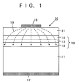
- Figure 1 shows a schematic cross section of one example of the AlGaInP light emitting device of this invention.
- Figure 2 shows a configuration example of the growth apparatus used for growing the layers by means of the MOVPE method.
- Figure 3 shows a schematic cross section of one example of conventional AlGaInP light emitting devices.
- a light emitting layer portion made of an AlGaInP double heterojunction structure or an AlGaInP single heterojunction structure is formed on a first conductivity-type GaAs substrate, and then a layer made of a second conductivity-type Al W Ga 1-W As 1-V P V mixed crystal (Al 0.7 Ga 0.3 As 0.97 P 0.03 , for example) which has the bandgap energy larger than the energy of photon emitted from the active layer of said light emitting layer portion, and has very good lattice-matching with the (Al B Ga 1-B ) 0.51 In 0.49 P mixed crystals (layers) constituting said light emitting layer portion, is formed as a current spreading layer on top of said light emitting layer portion.
- w and v are in the range of 0.45 ⁇ w ⁇ 1 and 0 ⁇ v ⁇ 0.08, respectively.
- the thickness of said Al W Ga 1-W As 1-V P V current spreading layer must be 3 micrometers or more in order to diffuse current effectively, and the thicker it is, the higher the brightness will be.
- heterojunction structure of said light emitting layer portion would be a double heterojunction structure comprising a first conductivity-type cladding layer made of the (Al x Ga 1-x ) 0.51 In 0.49 P mixed crystal, an active layer made of the (Al y Ga 1-y ) 0.51 In 0.49 P mixed crystal and a second conductivity-type cladding layer made of the (Al z Ga 1-z ) 0.51 In 0.49 P mixed crystal.
- x, y and z are set to satisfy the following relationships: 0 ⁇ y ⁇ 0.7, y ⁇ x, and y ⁇ z.
- Said w and v are set in the range of 0.45 ⁇ w ⁇ 1 and 0 ⁇ v ⁇ 0.08, respectively.
- a single heterojunction structure comprising an active layer made of the (Al y Ga 1-y ) 0.51 In 0.49 P mixed crystal and a second conductivity-type cladding layer made of the (Al z Ga 1-z ) 0.51 In 0.49 P mixed crystal can also be used.
- y and z are set to satisfy the following relationships: 0 ⁇ y ⁇ 0.7 and y ⁇ z.
- Said w and v are set in the range of 0.45 ⁇ w ⁇ 1 and 0 ⁇ v ⁇ 0.08, respectively.
- a specific example of mixed crystal which is in perfect lattice-matching with (Al B Ga 1-B ) 0.51 In 0.49 P constituting the light emitting layer portion would be Al 0.7 Ga 0.3 As 1-v P v mixed crystals with v of approximately 0.025.
- the current spreading layer provided between the light-emitting-side electrode (top surface electrode) and the AlGaInP light emitting layer portion is made of Al w Ga 1-w As 1-v P v mixed crystal which is in very good lattice-matching with the (Al B Ga 1-B ) 0.51 In 0.49 P mixed crystals (layers) constituting said light emitting layer portion. Therefore it is possible to significantly reduce the stress caused by the lattice-mismatch between the layers.
- This reduction of the internal stress makes it possible not only to sufficiently extend the life of said light emitting device but also to significantly reduce warping of the AlGaInP epitaxial wafer used for manufacturing said light emitting device.
- the AlGaInP light emitting device of this invention is described below by referring to Figure 1 and Figure 2.
- the layer structure of the light emitting layer portion there are, as described above, the AlGaInP double heterojunction structure, the AlGaInP single heterojunction structure and such.
- the layer structure of the light emitting layer portion is not essential for discussing formation of the current spreading layer, which is the subject of this invention, we have chosen the AlGaInP light emitting devices which have the AlGaInP double heterojunction structure for the purpose of description.
- FIG. 1 shows a schematic cross section of one example of the AlGaInP light emitting device of this invention.
- This light emitting device 30 has the following structure: An n-type (Al 0.7 Ga 0.3 ) 0.51 In 0.49 P cladding layer 12 (approximately 1 micrometer thick), an (Al y Ga 1-y ) 0.51 In 0.49 P active layer 13 (0 ⁇ y ⁇ 0.7, approximately 0.6 micrometers thick), a p-type (Al 0.7 Ga 0.3 ) 0.51 In 0.49 P cladding layer 14 (approximately 1 micrometer thick) and a p-type Al 0.7 Ga 0.3 As 0.97 P 0.03 current spreading layer 31 (3 micrometers thick or thicker) are formed, one after another, on an n-type GaAs substrate 11, and a p-side electrode 16 and an n-side electrode 17 are provided on said p-type current spreading layer 31 and on the bottom
- the MOVPE method For the method of growing the AlGaInP layers (the active layer and the cladding layers) and the AlGaAsP layer (current spreading layer), the MOVPE method is adopted.
- the material source for Al Ga, In, As and P, trimethyl aluminum (Al(CH3)3) , trimethyl gallium (Ga(CH3)3), trimethyl indium (In(CH3)3), arsine (AsH3) and phosphine (PH3), respectively, are used.
- As the n-type and p-type dopant sources hydrogen selenide (H2Se) and dimethyl zinc (Zn(CH3)2), respectively, are used.
- Figure 2 shows a configuration example of a growth apparatus used for growing the layers by means of the MOVPE method.
- Various vapors of metalorganic compounds of Group III metals and hydride gases of Group V elements are mixed and the obtained mixed-gas is fed into a process tube 20, with partial pressures and flow rates adjusted according to the composition of the growing layer, and then the desired growing layers are formed, one after another, on the n-type GaAs substrate 11 which is placed in the process tube 20.
- said layers 12, 13, 14 and 31 are formed on the n-type GaAs substrate 11, by supplying mixed source gases prepared in such a way that the supply ratio of the Group V element(s) and the Group III element(s) (V/III ratio) is 100, under the following growth conditions: a growth temperature of 710°C and a growth rate of 4 micrometers/hour.
- the epitaxial wafer thus obtained is made into elements to obtain the AlGaInP light emitting device 30 shown in Figure 1.
- Table 1 shows various characteristics of the AlGaInP light emitting devices and the epitaxial wafers used for manufacturing said AlGaInP light emitting devices of this invention for which the Al 0.7 Ga 0.3 As 0.97 P 0.03 mixed crystal is used for the current spreading layer, in comparison with those of the comparative example.
- the AlGaInP light emitting devices of the comparative example is the same as those for the example except for the fact that Al 0.7 Ga 0.3 As mixed crystal is used as the material for the current spreading layer.
- the example indicates that enough high brightness can be obtained when the thickness of the current spreading layer is 3 micrometers or more, and that the brightness becomes higher as the thickness of the current spreading layer increases. That is, if the thickness of the current spreading layer is 3 micrometers or more, the current from the p-side electrode 16 is effectively spread over the whole area of the active layer, resulting in enough efficient light emission.
- the comparative example indicates that, due to the stress caused by the lattice-mismatch, the brightness decreases, rather than increasees, as the thickness of the current spreading layer increases.
- the AlGaInP light emitting device of this example has a much improved life and the epitaxial wafer used for manufacturing said AlGaInP light emitting device has less warping, when compared with conventional ones. Based on this finding, it can be said that, by forming, on top of the light emitting layer portion 18, the current spreading layer 31 made of Al w Ga 1-w As 1-v P v mixed crystal which has very good lattice-matching with the (Al B Ga 1-B ) 0.51 In 0.49 P mixed crystal (layer) constituting said light emitting layer portion 18, it is possible to significantly reduce the stress caused by the lattice-mismatch.
- the AlGaInP light emitting device of this invention is a light emitting device which has high brightness, i.e. effective current spreading, as well as a long life and high reliability.
- an AlGaInP light emitting device comprising an n-type cladding layer, an active layer, a p-type cladding layer and a p-type current spreading layer formed, one after another, on an n-type GaAs substrate.
- a single heterojunction structure can also be used. Needless to say, the conditions in the example described above can be changed within the range which is consistent with the purpose of this invention.
- this invention by providing a current spreading layer which is in good lattice-matching with the (Al B Ga 1-B ) 0.51 In 0.49 P layers constituting said light emitting layer portion, makes it possible to obtain an AlGaInP light emitting device which has a long life and high reliability, showing no deterioration of the light emitting characteristics even by a light emitting operation over a long term.
Landscapes
- Led Devices (AREA)
Applications Claiming Priority (2)
| Application Number | Priority Date | Filing Date | Title |
|---|---|---|---|
| JP15416993A JP2900754B2 (ja) | 1993-05-31 | 1993-05-31 | AlGaInP系発光装置 |
| JP154169/93 | 1993-05-31 |
Publications (3)
| Publication Number | Publication Date |
|---|---|
| EP0627772A2 true EP0627772A2 (de) | 1994-12-07 |
| EP0627772A3 EP0627772A3 (de) | 1995-03-01 |
| EP0627772B1 EP0627772B1 (de) | 1997-09-03 |
Family
ID=15578344
Family Applications (1)
| Application Number | Title | Priority Date | Filing Date |
|---|---|---|---|
| EP94107562A Expired - Lifetime EP0627772B1 (de) | 1993-05-31 | 1994-05-16 | Licht emittierende Halbleitervorrichtung aus AlGaInP |
Country Status (4)
| Country | Link |
|---|---|
| US (1) | US5444269A (de) |
| EP (1) | EP0627772B1 (de) |
| JP (1) | JP2900754B2 (de) |
| DE (1) | DE69405294T2 (de) |
Cited By (5)
| Publication number | Priority date | Publication date | Assignee | Title |
|---|---|---|---|---|
| EP0703630A3 (de) * | 1994-09-22 | 1996-07-31 | Shinetsu Handotai Kk | Lichtemittierende Halbleitervorrichtung |
| EP0720242A3 (de) * | 1994-12-27 | 1997-07-30 | Shinetsu Handotai Kk | Lichtemittierende Halbleitervorrichtung aus AlGaInP |
| US5726465A (en) * | 1995-10-09 | 1998-03-10 | Temic Telefunken Microelectronic Gmbh | Light emitting diode |
| EP0727827A3 (de) * | 1995-02-15 | 1998-07-01 | Mitsubishi Cable Industries, Ltd. | Licht emittierende Halbleitervorrichtung |
| GB2338591A (en) * | 1998-05-29 | 1999-12-22 | Lite On Electronics Inc | Transparent LED window layer formed by a super-lattice |
Families Citing this family (6)
| Publication number | Priority date | Publication date | Assignee | Title |
|---|---|---|---|---|
| JP3122324B2 (ja) * | 1995-02-20 | 2001-01-09 | 三菱電線工業株式会社 | 半導体発光素子 |
| JP3233569B2 (ja) * | 1996-03-22 | 2001-11-26 | シャープ株式会社 | 半導体発光素子 |
| US5835521A (en) * | 1997-02-10 | 1998-11-10 | Motorola, Inc. | Long wavelength light emitting vertical cavity surface emitting laser and method of fabrication |
| JP3472714B2 (ja) * | 1999-01-25 | 2003-12-02 | シャープ株式会社 | 半導体発光素子の製造方法 |
| DE10329515B9 (de) | 2003-06-30 | 2022-01-20 | OSRAM Opto Semiconductors Gesellschaft mit beschränkter Haftung | Elektromagnetische Strahlung emittierendes Bauelement und Verfahren zu dessen Herstellung |
| JP2007042751A (ja) * | 2005-08-01 | 2007-02-15 | Hitachi Cable Ltd | 半導体発光素子 |
Family Cites Families (13)
| Publication number | Priority date | Publication date | Assignee | Title |
|---|---|---|---|---|
| JPS5511310A (en) * | 1978-07-10 | 1980-01-26 | Hitachi Ltd | Semiconductor laser element |
| FR2508244A1 (fr) * | 1981-06-19 | 1982-12-24 | Thomson Csf | Laser a semi-conducteur a courte longueur d'onde |
| US4706255A (en) * | 1985-05-20 | 1987-11-10 | Xerox Corporation | Phased array semiconductor laser with preferred emission in the fundamental supermode |
| JPH0654821B2 (ja) * | 1985-06-05 | 1994-07-20 | 日本電気株式会社 | 半導体発光素子 |
| US4727557A (en) * | 1985-12-30 | 1988-02-23 | Xerox Corporation | Phased array semiconductor lasers fabricated from impurity induced disordering |
| JP2618677B2 (ja) * | 1988-03-24 | 1997-06-11 | 三菱電線工業株式会社 | 半導体発光装置 |
| JPH0298984A (ja) * | 1988-10-06 | 1990-04-11 | Denki Kagaku Kogyo Kk | InGaAlp 半導体発光素子 |
| US5048035A (en) * | 1989-05-31 | 1991-09-10 | Kabushiki Kaisha Toshiba | Semiconductor light emitting device |
| JPH0394481A (ja) * | 1989-09-07 | 1991-04-19 | Ricoh Co Ltd | アレイ状半導体発光装置 |
| US5008718A (en) * | 1989-12-18 | 1991-04-16 | Fletcher Robert M | Light-emitting diode with an electrically conductive window |
| JPH03227077A (ja) * | 1990-01-31 | 1991-10-08 | Nec Corp | 発光ダイオード |
| US5202285A (en) * | 1990-04-26 | 1993-04-13 | Fujitsu Limited | Semiconductor laser having double heterostructure and method of producing same |
| JP3251603B2 (ja) * | 1990-08-20 | 2002-01-28 | 株式会社東芝 | 半導体発光装置 |
-
1993
- 1993-05-31 JP JP15416993A patent/JP2900754B2/ja not_active Expired - Fee Related
-
1994
- 1994-05-16 EP EP94107562A patent/EP0627772B1/de not_active Expired - Lifetime
- 1994-05-16 DE DE69405294T patent/DE69405294T2/de not_active Expired - Fee Related
- 1994-05-31 US US08/251,370 patent/US5444269A/en not_active Expired - Fee Related
Cited By (7)
| Publication number | Priority date | Publication date | Assignee | Title |
|---|---|---|---|---|
| EP0703630A3 (de) * | 1994-09-22 | 1996-07-31 | Shinetsu Handotai Kk | Lichtemittierende Halbleitervorrichtung |
| US5600158A (en) * | 1994-09-22 | 1997-02-04 | Shin-Etsu Handotai Co., Ltd. | Semiconductor light emitting device with current spreading layer |
| EP0720242A3 (de) * | 1994-12-27 | 1997-07-30 | Shinetsu Handotai Kk | Lichtemittierende Halbleitervorrichtung aus AlGaInP |
| US5739553A (en) * | 1994-12-27 | 1998-04-14 | Shin-Etsu Handotai, Co., Ltd. | Algainp light-emitting device |
| EP0727827A3 (de) * | 1995-02-15 | 1998-07-01 | Mitsubishi Cable Industries, Ltd. | Licht emittierende Halbleitervorrichtung |
| US5726465A (en) * | 1995-10-09 | 1998-03-10 | Temic Telefunken Microelectronic Gmbh | Light emitting diode |
| GB2338591A (en) * | 1998-05-29 | 1999-12-22 | Lite On Electronics Inc | Transparent LED window layer formed by a super-lattice |
Also Published As
| Publication number | Publication date |
|---|---|
| JP2900754B2 (ja) | 1999-06-02 |
| JPH06342936A (ja) | 1994-12-13 |
| EP0627772B1 (de) | 1997-09-03 |
| US5444269A (en) | 1995-08-22 |
| DE69405294D1 (de) | 1997-10-09 |
| EP0627772A3 (de) | 1995-03-01 |
| DE69405294T2 (de) | 1998-04-02 |
Similar Documents
| Publication | Publication Date | Title |
|---|---|---|
| US5442203A (en) | Semiconductor light emitting device having AlGaAsP light reflecting layers | |
| EP0702414B1 (de) | Lichtemittierende Halbleitervorrichtungen | |
| US5747832A (en) | Light-emitting gallium nitride-based compound semiconductor device | |
| US5625202A (en) | Modified wurtzite structure oxide compounds as substrates for III-V nitride compound semiconductor epitaxial thin film growth | |
| US6649942B2 (en) | Nitride-based semiconductor light-emitting device | |
| US5600158A (en) | Semiconductor light emitting device with current spreading layer | |
| US6107648A (en) | Semiconductor light emitting device having a structure which relieves lattice mismatch | |
| US20080083919A1 (en) | Light emitting diode | |
| JPH0897468A (ja) | 半導体発光素子 | |
| EP0627772B1 (de) | Licht emittierende Halbleitervorrichtung aus AlGaInP | |
| EP0617470A2 (de) | Licht emittierende Halbleitervorrichtung und Verfahren zu ihrer Herstellung | |
| US5739553A (en) | Algainp light-emitting device | |
| EP2101361B1 (de) | Lichtemittierendes Halbleiterbauelement und Herstellungsverfahren dafür und Epitaxialwafer | |
| JP3355901B2 (ja) | 化合物半導体エピタキシャルウエーハ | |
| JPH0945959A (ja) | 発光素子 | |
| JP3146637B2 (ja) | エピタキシャルウェーハ及び黄色発光ダイオード | |
| JP2937060B2 (ja) | AlGaInP系発光装置 | |
| JP4376373B2 (ja) | 半導体発光素子用エピタキシャルウェハ、その製造方法および半導体発光素子 | |
| JP2937054B2 (ja) | AlGaInP系発光装置 | |
| JPH05308153A (ja) | エピタキシャルウェーハ及び発光ダイオード | |
| JPH05347431A (ja) | 半導体素子用基板および半導体素子 | |
| JPH0738152A (ja) | 半導体発光素子 | |
| JPWO1997045881A1 (ja) | 半導体発光素子およびその製法 |
Legal Events
| Date | Code | Title | Description |
|---|---|---|---|
| PUAI | Public reference made under article 153(3) epc to a published international application that has entered the european phase |
Free format text: ORIGINAL CODE: 0009012 |
|
| AK | Designated contracting states |
Kind code of ref document: A2 Designated state(s): DE FR GB |
|
| PUAL | Search report despatched |
Free format text: ORIGINAL CODE: 0009013 |
|
| AK | Designated contracting states |
Kind code of ref document: A3 Designated state(s): DE FR GB |
|
| 17P | Request for examination filed |
Effective date: 19950830 |
|
| GRAG | Despatch of communication of intention to grant |
Free format text: ORIGINAL CODE: EPIDOS AGRA |
|
| 17Q | First examination report despatched |
Effective date: 19961120 |
|
| GRAH | Despatch of communication of intention to grant a patent |
Free format text: ORIGINAL CODE: EPIDOS IGRA |
|
| GRAH | Despatch of communication of intention to grant a patent |
Free format text: ORIGINAL CODE: EPIDOS IGRA |
|
| GRAA | (expected) grant |
Free format text: ORIGINAL CODE: 0009210 |
|
| AK | Designated contracting states |
Kind code of ref document: B1 Designated state(s): DE FR GB |
|
| REF | Corresponds to: |
Ref document number: 69405294 Country of ref document: DE Date of ref document: 19971009 |
|
| ET | Fr: translation filed | ||
| PLBE | No opposition filed within time limit |
Free format text: ORIGINAL CODE: 0009261 |
|
| STAA | Information on the status of an ep patent application or granted ep patent |
Free format text: STATUS: NO OPPOSITION FILED WITHIN TIME LIMIT |
|
| 26N | No opposition filed | ||
| PGFP | Annual fee paid to national office [announced via postgrant information from national office to epo] |
Ref country code: FR Payment date: 19990511 Year of fee payment: 6 |
|
| PGFP | Annual fee paid to national office [announced via postgrant information from national office to epo] |
Ref country code: GB Payment date: 19990512 Year of fee payment: 6 |
|
| PG25 | Lapsed in a contracting state [announced via postgrant information from national office to epo] |
Ref country code: GB Free format text: LAPSE BECAUSE OF NON-PAYMENT OF DUE FEES Effective date: 20000516 |
|
| GBPC | Gb: european patent ceased through non-payment of renewal fee |
Effective date: 20000516 |
|
| PG25 | Lapsed in a contracting state [announced via postgrant information from national office to epo] |
Ref country code: FR Free format text: LAPSE BECAUSE OF NON-PAYMENT OF DUE FEES Effective date: 20010131 |
|
| REG | Reference to a national code |
Ref country code: FR Ref legal event code: ST |
|
| PGFP | Annual fee paid to national office [announced via postgrant information from national office to epo] |
Ref country code: DE Payment date: 20030529 Year of fee payment: 10 |
|
| PG25 | Lapsed in a contracting state [announced via postgrant information from national office to epo] |
Ref country code: DE Free format text: LAPSE BECAUSE OF NON-PAYMENT OF DUE FEES Effective date: 20041201 |