EP0632341A2 - Bilderzeugungsgerät - Google Patents
Bilderzeugungsgerät Download PDFInfo
- Publication number
- EP0632341A2 EP0632341A2 EP94304689A EP94304689A EP0632341A2 EP 0632341 A2 EP0632341 A2 EP 0632341A2 EP 94304689 A EP94304689 A EP 94304689A EP 94304689 A EP94304689 A EP 94304689A EP 0632341 A2 EP0632341 A2 EP 0632341A2
- Authority
- EP
- European Patent Office
- Prior art keywords
- transfer
- width
- charging
- layer
- transfer member
- Prior art date
- Legal status (The legal status is an assumption and is not a legal conclusion. Google has not performed a legal analysis and makes no representation as to the accuracy of the status listed.)
- Granted
Links
- 238000012546 transfer Methods 0.000 claims abstract description 264
- 239000010410 layer Substances 0.000 claims abstract description 131
- 239000000463 material Substances 0.000 claims abstract description 92
- 239000002344 surface layer Substances 0.000 claims abstract description 24
- 238000011161 development Methods 0.000 claims description 22
- 238000007599 discharging Methods 0.000 claims description 18
- 230000014759 maintenance of location Effects 0.000 claims 1
- 238000000034 method Methods 0.000 description 8
- 238000000926 separation method Methods 0.000 description 8
- 230000005684 electric field Effects 0.000 description 6
- 230000002093 peripheral effect Effects 0.000 description 6
- 229920002943 EPDM rubber Polymers 0.000 description 5
- 230000000694 effects Effects 0.000 description 5
- 229920002981 polyvinylidene fluoride Polymers 0.000 description 4
- 229910052782 aluminium Inorganic materials 0.000 description 3
- XAGFODPZIPBFFR-UHFFFAOYSA-N aluminium Chemical compound [Al] XAGFODPZIPBFFR-UHFFFAOYSA-N 0.000 description 3
- 210000000078 claw Anatomy 0.000 description 3
- 239000003086 colorant Substances 0.000 description 3
- 230000003247 decreasing effect Effects 0.000 description 3
- 239000013013 elastic material Substances 0.000 description 3
- 230000006872 improvement Effects 0.000 description 3
- 230000001105 regulatory effect Effects 0.000 description 3
- 230000000717 retained effect Effects 0.000 description 3
- 239000007787 solid Substances 0.000 description 3
- JOYRKODLDBILNP-UHFFFAOYSA-N Ethyl urethane Chemical compound CCOC(N)=O JOYRKODLDBILNP-UHFFFAOYSA-N 0.000 description 2
- 239000004677 Nylon Substances 0.000 description 2
- 238000004140 cleaning Methods 0.000 description 2
- 230000006870 function Effects 0.000 description 2
- 229920001778 nylon Polymers 0.000 description 2
- 230000008569 process Effects 0.000 description 2
- 239000011800 void material Substances 0.000 description 2
- OKTJSMMVPCPJKN-UHFFFAOYSA-N Carbon Chemical compound [C] OKTJSMMVPCPJKN-UHFFFAOYSA-N 0.000 description 1
- 239000004642 Polyimide Substances 0.000 description 1
- 229920006311 Urethane elastomer Polymers 0.000 description 1
- 230000009471 action Effects 0.000 description 1
- 229910021417 amorphous silicon Inorganic materials 0.000 description 1
- 230000002238 attenuated effect Effects 0.000 description 1
- 230000015572 biosynthetic process Effects 0.000 description 1
- 229910052799 carbon Inorganic materials 0.000 description 1
- 238000011109 contamination Methods 0.000 description 1
- 238000013461 design Methods 0.000 description 1
- 230000006866 deterioration Effects 0.000 description 1
- 239000003989 dielectric material Substances 0.000 description 1
- 229920001971 elastomer Polymers 0.000 description 1
- 238000001704 evaporation Methods 0.000 description 1
- 230000008020 evaporation Effects 0.000 description 1
- 238000010348 incorporation Methods 0.000 description 1
- 238000011835 investigation Methods 0.000 description 1
- 229910052751 metal Inorganic materials 0.000 description 1
- 239000002184 metal Substances 0.000 description 1
- 238000012986 modification Methods 0.000 description 1
- 230000004048 modification Effects 0.000 description 1
- 239000004033 plastic Substances 0.000 description 1
- 229920003023 plastic Polymers 0.000 description 1
- 229920001084 poly(chloroprene) Polymers 0.000 description 1
- 229920001721 polyimide Polymers 0.000 description 1
- 238000011112 process operation Methods 0.000 description 1
- 238000005096 rolling process Methods 0.000 description 1
- 229920002379 silicone rubber Polymers 0.000 description 1
- 239000004945 silicone rubber Substances 0.000 description 1
- 239000000758 substrate Substances 0.000 description 1
- 229920002803 thermoplastic polyurethane Polymers 0.000 description 1
Images



Classifications
-
- G—PHYSICS
- G03—PHOTOGRAPHY; CINEMATOGRAPHY; ANALOGOUS TECHNIQUES USING WAVES OTHER THAN OPTICAL WAVES; ELECTROGRAPHY; HOLOGRAPHY
- G03G—ELECTROGRAPHY; ELECTROPHOTOGRAPHY; MAGNETOGRAPHY
- G03G15/00—Apparatus for electrographic processes using a charge pattern
- G03G15/01—Apparatus for electrographic processes using a charge pattern for producing multicoloured copies
-
- G—PHYSICS
- G03—PHOTOGRAPHY; CINEMATOGRAPHY; ANALOGOUS TECHNIQUES USING WAVES OTHER THAN OPTICAL WAVES; ELECTROGRAPHY; HOLOGRAPHY
- G03G—ELECTROGRAPHY; ELECTROPHOTOGRAPHY; MAGNETOGRAPHY
- G03G15/00—Apparatus for electrographic processes using a charge pattern
- G03G15/14—Apparatus for electrographic processes using a charge pattern for transferring a pattern to a second base
- G03G15/16—Apparatus for electrographic processes using a charge pattern for transferring a pattern to a second base of a toner pattern, e.g. a powder pattern, e.g. magnetic transfer
- G03G15/1665—Apparatus for electrographic processes using a charge pattern for transferring a pattern to a second base of a toner pattern, e.g. a powder pattern, e.g. magnetic transfer by introducing the second base in the nip formed by the recording member and at least one transfer member, e.g. in combination with bias or heat
- G03G15/167—Apparatus for electrographic processes using a charge pattern for transferring a pattern to a second base of a toner pattern, e.g. a powder pattern, e.g. magnetic transfer by introducing the second base in the nip formed by the recording member and at least one transfer member, e.g. in combination with bias or heat at least one of the recording member or the transfer member being rotatable during the transfer
- G03G15/1685—Structure, details of the transfer member, e.g. chemical composition
-
- G—PHYSICS
- G03—PHOTOGRAPHY; CINEMATOGRAPHY; ANALOGOUS TECHNIQUES USING WAVES OTHER THAN OPTICAL WAVES; ELECTROGRAPHY; HOLOGRAPHY
- G03G—ELECTROGRAPHY; ELECTROPHOTOGRAPHY; MAGNETOGRAPHY
- G03G15/00—Apparatus for electrographic processes using a charge pattern
- G03G15/01—Apparatus for electrographic processes using a charge pattern for producing multicoloured copies
- G03G15/0105—Details of unit
- G03G15/0131—Details of unit for transferring a pattern to a second base
Definitions
- the present invention relates to a color image forming apparatus in which respective color toner images formed on an image bearing member having an electrophotographic photosensitive member are sequentially transferred onto a transfer material to provide a color image.
- a toner image is formed on an image bearing member through charging, exposure and development, and the toner image is transferred onto a transfer material after each color toner image is formed, and this is repeated for the respective colors, by which a superposed color image is formed on the transfer material.
- Examples of the color image forming apparatus are disclosed in German Patent No. 2607727, Japanese Laid-Open Patent Application No. 50-50935 or the like.
- Figure 4 is a longitudinal sectional view of an example of such a color image forming apparatus. As shown, the apparatus is provided with an electrophotographic photosensitive drum 1 as an image bearing member.
- a primary charger 3 in the form of a roller electrode, rotary type developing device 4 having a plurality of developing units, a transfer device 10A and a cleaning device 26.
- a laser diode 11 constituting an exposure device, a polygonal mirror 13 rotated by a high speed motor 12, and a lens 14 and a reflection mirror 15.
- the photosensitive drum 1 comprises an aluminum cylinder having a diameter of 40 mm and an organic photoconductor (OPC) thereon.
- the photoconductor may be an amorphous silicon, CdS, Se or the like.
- the photosensitive drum 1 is rotated in a direction indicated by an arrow at a peripheral speed of 100 mm/sec by an unshown driving means.
- the developing device 4 is provided with a supporting member 9 rotatable about a shaft 9a, the supporting member 9 supports an yellow developing device 4a, a magenta developing device 4b, a cyan developing device 4c and a black developing device 4d.
- the developing devices 4a, 4b, 4c and 4d contain one component developers, more particularly, yellow toner, magenta toner, cyan toner, black toner, respectively.
- each of the developing devices 4a, 4b, 4c and 4d there is provided a developing sleeve 8a, 8b, 8c and 8d as the developer carrying member in the openings 5a, 5b, 5c and 5d.
- a developing sleeve 8a, 8b, 8c and 8d there are application roller 6a, 6b, 6c and 6d, and toner regulating member 7a, 7b, 7c and 7d.
- toner is applied by the application roller 6a, 6b, 6c and 6d on the developing sleeve 8a, 8b, 8c and 8d.
- the toner regulating member 7a, 7b, 7c and 7d regulates the toner and applies triboelectric charge to the toner to provide a thin toner layer on the developing speed 8a, 8b, 8c and 8d.
- the toner regulating members 7a - 7d are preferably made of a material charged to the polarity opposite from that of the toner.
- the material may be nylon or the like, and when it is to be charged to the positive polarity, silicone rubber or the like is preferable.
- the peripheral speed of the developing sleeve 8a - 8d of each of the developing devices 4a - 4d is preferably determined so as to be 1.0 - 2.0 times the peripheral speed of the photosensitive drum 1.
- the opening 5a - 5d is always faced to the photosensitive drum 1.
- the transfer device 10a is provided with a transfer drum 10 as a transfer material carrying member, and around the transfer drum 10, there are attraction roller 23, charge removing discharger 2, separation claws, cleaner 27 and discharging roller 28.
- the transfer drum 10 is provided with grippers 22 at a position on the outer peripheral for gripping the transfer material.
- the transfer drum 10 is rotated in the direction indicated by an arrow substantially at the same peripheral speed of the photosensitive drum, by an unshown driving means.
- a transfer material is fed from a transfer material cassette 17 in synchronism with an image on the photosensitive drum 1, by a pickup roller 18.
- the transfer drum 10 feeds the transfer material to the image transfer station.
- the transfer sheet in the transfer station receives the toner image of each of the colors from the photosensitive drum 1 by the transfer voltage applied between the transfer drum 10 and the photosensitive drum 1 by an unshown voltage source.
- the image forming methods are generally classified into a regular development method in which non-exposed area of the photosensitive member receives the toner, and a reverse development in which the area exposed to light receives the toner image.
- a regular development method in which non-exposed area of the photosensitive member receives the toner
- a reverse development in which the area exposed to light receives the toner image.
- the photosensitive drum 1 uniformly charged by a charging means 3 is exposed to image light, and the toner is deposited on the non-exposed portion of the charged area, and therefore, the charge polarity of the toner is opposite from that of the polarity provided by the charging means 3.
- the transfer drum 10 is supplied with a transfer voltage having the same polarity as the charge of the photosensitive member and of a voltage level having an absolute value larger than that of the primary charge, so that the toner is transferred from the photosensitive drum 1 onto the transfer sheet.
- the photosensitive drum 1 uniformly charged by the charging means 3 receives the toner only at the exposed portion of the charged area of the photosensitive drum 1. Therefore, the polarity of the toner is the same as the polarity of the charge provided by the charging means 3, contrary to the case of the regular development.
- the transfer drum 10 is supplied with a transfer voltage of the polarity opposite from that of the charged polarity of the photosensitive drum 1, so that the toner is transferred from the photosensitive drum 1 onto the transfer material.
- the development and transfer operations are repeated by the developing devices 4a, 4b, 4c and 4d, and the four color toner images are superimposed on the transfer material, in order to provide the color image.
- an attraction roller 23 is disposed adjacent to the sheet feeding portion of the transfer material to the transfer drum 10 to apply an attraction voltage, by which the transfer material is electrostatically attracted beforehand after it is gripped by the gripper.
- the transfer sheet having been subjected to the transfer operation to receive the four color toner images is electrically discharged by discharger 2 disposed adjacent to the transfer drum 10, and thereafter, it is separated from the transfer drum 10 by the downstream separation claws 24, and it is fed to an image fixing device 25.
- the four color toner images are fixed by heat and pressure to fix the mixed toner images on the transfer material into a permanent full-color image. Thereafter, it is discharged outside the image forming apparatus.
- the transfer drum 10 from which the transfer material has been removed is cleaned by a cleaner 27 having a cleaning member such as a fur brush or web or the like, so that the toner remaining on the surface is removed.
- the discharging roller 28 is contacted to the transfer drum 10 so as to discharge the surface of the transfer drum by an AC voltage (the AC voltage biased with a DC voltage) applied to the discharging roller 28.
- a blank is provided at an end of the transfer material.
- a sheet which is larger than a regular size may be used (for example, a blead size for a letter size is larger by 1 inch and by 1/2 inch approximately, in the vertical and horizontal directions, respectively). In this case, a blank is formed around the sheet. The portion without the blank is called effective image area.
- width of the effective image area in the direction of an axis of the photosensitive drum Exposure width in the case of reverse development
- Wd a width of development of the developing device
- Wc charging width of the charging means
- the resultant image does not have a missing part.
- the transfer area is larger than the effective image width Wl.
- the transfer material width Wp development width Wd or charging width Wc.
- the transfer apparatus of a transfer drum type there are two types in one of which a thin dielectric sheet is formed into a hollow cylinder (hollow transfer drum) and an electroconductive elastic material 10b or the like is provided behind a thin dielectric sheet 10c, and a voltage is applied to an electroconductive base 10a (solid transfer drum).
- the charging is effected by corona charging or the like to the front or back side of the drum for each of the stations for attraction, transfer and separation, and therefore, the apparatus becomes complicated.
- corona charging or the like to the front or back side of the drum for each of the stations for attraction, transfer and separation, and therefore, the apparatus becomes complicated.
- this type is widely used.
- the bias voltage is applied to the conductive base 10a, and therefore, the structure is simple, but the respective stations are not electrically independent.
- the transfer, attraction, separation or other process operations are carried out by transfer of electric charge between the transfer drum, the attraction roller, the discharging roller 28 and the dielectric sheet 10c, the transfer material, with the conductive elastic material functioning as an opposite electrode, and therefore, as compared with the hollow structure, voltage conditions and the voltage application timings are more limited than in the hollow type.
- the auxiliary attraction force due to the attraction roller 28 is not so strong as compared with the attraction or the like due to the corona charge by the hollow transfer drum.
- the electric charge is applied to the surface of the transfer material to the surface of the photosensitive drum 1 and the transfer drum 10, and the attraction is effected by the charge and the charge induced to the backside of the dielectric sheet 10c.
- the transfer material is retained on the transfer drum 10.
- the photosensitive drum 1 as a charge supply source and an electroconductive layer 10b functioning as an opposite electrode are overlapped in the entire longitudinal direction of the transfer material for the purpose of attraction.
- the charging width Wc is not more than the width Wb of the transfer material, no particular inconvenience occurs in the case of the regular development. However, if this is so under the condition that the above-described conditions are satisfied, the attraction force at an end of the transfer material is weak in the case of reverse development. If a part of the transfer material is raised from the transfer drum, a deviation occurs between the transfer drum 10 and the transfer material when the color toner images are sequentially overlaid on the transfer material through the transfer step, even to the extent that the transfer material is separated. In the case of solid transfer drum, the backside charge moves laterally through the electroconductive layer, the sheet is peeled gradually from the raised portion.
- the potential of the photosensitive drum in the neighborhood of the opposite ends of the transfer material is non-charging potential.
- the potential is approx. 0 volt actually. This is substantially the same as the light potential in the background in the image region, and therefore, the attraction at the end may be strong (the same polarity charge may be effected by the transfer drum as the case may be).
- a strong electric field as compared with the dark potential in the portion having the toner is formed between the electroconductive layer 10b supplied with a bias voltage having an absolute value larger than the charge potential and having the same polarity as that, and therefore, the corresponding sufficient electric charge is applied or induced to the transfer material and the dielectric layer 10c. Therefore, the peripheral of the transfer sheet is strongly attracted.
- the potential on the photosensitive drum 1 adjacent the opposite end portions of the transfer material is approx. 0 volt (non-charging potential) (it may be charged to the polarity opposite from the dark potential by the transfer drum as the case may be).
- the white background portion in the image area has a dark potential. Therefore, when the transfer bias voltage having the polarity opposite from that the dark potential, that is, the transfer potential, is applied to the electroconductive layer 10b during the transfer operation, the electric field between the photosensitive member 1 and the conductive layer 10b is weak at the end portions of the transfer material relatively as compared with the image region. For this reason, the sufficient electric charge is not applied or induced with the result of weak attraction at the periphery of the transfer material. Therefore, as the superimposing transfer operations are carried out, the transfer material is raised or removed from the transfer drum.
- an image forming apparatus comprising: an electrophotographic photosensitive member; charging means for charging the photosensitive member to form an electrostatic latent image on the photosensitive member; exposure means for exposing the photosensitive member to image light; developing means for developing the latent image with toner; a transfer member contactable to the photosensitive member at a transfer position, the transfer member comprising an electrically conductive base, a high resistance surface layer, and a low resistance or intermediate resistance conductive layer between the conductive base and the surface layer; and transfer voltage applying means for applying a transfer voltage to the transfer member; wherein Ws > Wt > Wp > Wl is satisfied, where Ws is a width of a photosensitive layer measured in a direction perpendicular to a movement direction of the photosensitive member, Wl is an image exposure width of the exposure means, Wp is a width of a transfer material usable with the image forming apparatus, and Wt is an overlapping width between a charging width of the charging means and the width of the conductive layer of
- Figure 1 is a top plan view illustrating dimensional relationship among various parts in an apparatus according to a first embodiment of the present invention.
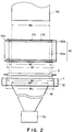
- Figure 2 is a similar view in the apparatus according to a second embodiment.
- Figure 3 is a similar view of an apparatus according to a third embodiment of the present invention.
- Figure 4 is a similar view of an apparatus according to a fifth embodiment of the present invention.
- Figure 5 is a sectional view of an image forming apparatus usable with the present invention.
- Figure 6 illustrates a rotary developing apparatus used in the apparatus of Figure 5.
- Figure 1 illustrates an embodiment 1 and shows a relationship in a width direction (scanning direction) of the apparatus shown in Figure 5.
- the description will be made as to the case using an OPC photosensitive member 31 having a negative charging property, as the photosensitive drum 1.
- the photosensitive member 31 is uniformly charged to the negative polarity by a charging roller 3 of a roller electrode type in rolling contact with the photosensitive member 31.
- the charging roller 3 may comprise an electroconductive elastic layer of EPDM or the like having a surface layer of urethane rubber or nylon. The total resistance thereof is 105 - 107 approximately.
- the charging roller 3 is supplied with a voltage in the form of a DC biased AC.
- the bias voltage is provided by superposing a DC of 720 V and an AC of 1800 Vpp (peak-to-peak voltage). By this, the photosensitive drum 1 is uniformly charged to approx. -700 V.
- the exposure apparatus 32 produces a scanning beam 16 by a laser diode 11 or a polygonal mirror 13 ( Figure 5) or the like, and scans the photosensitive drum 1 in a main scan direction with an image width Wl.
- the surface potential of the portion exposed to the beam attenuates to approx. -100 V, and the attenuated region receives the negatively charged toner.
- the toner image after the development is transferred onto the transfer material 30 through the transfer drum, the transfer material 30 having been retained on the transfer drum.
- the transfer drum 10 comprises an electrically conductive base 10a of aluminum or the like and an electrically conductive elastic layer 10b of foamed EPDM rubber having a width Wf, thickness of 5 mm, a hardness of 80 (Asker F) and a volume resistivity of not more than 106 ohm.cm, on the conductive base 10a, and a surface layer 10c of urethane dielectric layer having a volume resistivity of 1014 - 1015 ohm.cm and a thickness of approx. 40 ⁇ m.
- the contact between the transfer drum 1 and the transfer drum 10 is carried out by an abutment portion 10d of an insulating flange at each end of the transfer drum 10.
- the transfer voltage VT is increased gradually from +750 V for the first color, and the voltage is sequentially added by 250 V for the second and subsequent colors.
- the potential of the photosensitive drum 1 is substantially 0 V, and therefore, the faced surfaces of the photosensitive drum 1 and the conductive layer 10b, are subjected to weak electric field provided only by the transfer voltage VT.
- Wt Wf, because Wc > Wf in this example
- the conditions of various members are selected so as to satisfy the following: Ws > Wt > Wp > Wl where Ws is a width of the photosensitive layer, Wp is a maximum width of the transfer material, and Wl is a width of image exposure.
- the neighborhood of the ends of the transfer material are width in the width Wt, and sufficient negative charge is applied from the photosensitive layer 31 to the surface of the transfer material, and simultaneously sufficient positive charge is induced to the backside of the dielectric layer 10c, and therefore, the transfer material is not deviated or raised even if four color sequential transfer operation is carried out.
- the conductive elastic layer with Wf is larger than charging width Wc.
- dielectric layer 10c of urethane resin is provided on the elastic layer 10b of the foamed EPDM rubber.
- the dielectric layer 10f is formed by flexible sheet material of PVdF or polyimide in place of urethane material.
- the structure shown in Figure 2 that is, the structure satisfying the following (2) and (3) is preferable: Ws > Wc ⁇ Wf > Wp Wi ⁇ Wf
- the surface potential of the photosensitive layer can be made uniformly equal to the dark potential at the surface faced to the end portion of the elastic layer 10b, in addition to the attraction effect of the transfer material in Example 1. More particularly, the photosensitive layer 31 is subjected to the negative and positive charges alternately by the elastic layer 10b which is a transfer electrode and by the charging roller 3 adjacent to the end portions of the elastic layer 10b of the photosensitive layer 31. Then, the charge up to the positive polarity occurring when only the transfer electrode is faced, can be prevented. For this reason, the damage such as charge memory, of the OPC photosensitive layer 31 having the negative charging polarity, can be suppressed.
- the surface layer 10f is of PVdF sheet having a thickness of 70 ⁇ m; the maximum transfer material width is 210 mm; conductive elastic layer width Wf is 220 mm; charging width Wc is 226 mm; the width of PVdF which is a dielectric surface layer Wi is 246 mm; and the photosensitive layer width Ws is 246 mm. They are disposed so that the centers are substantially on line. It has been confirmed then that the positive polarity charging of the photosensitive layer adjacent the end portions of the conductive elastic layer 10b could be prevented while maintaining good attraction property of the transfer material 30. In addition, the discharging to the photosensitive layer 31 from end portions of the electroconductive base 10a or the end portions of the conductive elastic layer 10b, could be prevented.
- the width of the conductive elastic layer 10a is wider than the elastic layer 10b, but Figure 1 arrangement is usable. In such a case, the discharge from the conductive base 10a to the photosensitive drum 1 is not a problem even if there is no dielectric layer 10c.
- photosensitive layer width Ws > dielectric layer width Wi, but Ws ⁇ Wi is usable.
- the charging by the charging member 3 and the charging at the transfer operation have the same polarity, and therefore, even if Wc ⁇ Wf in inequation (2), is used, the photosensitive member 31 is free of the charging memory or the like.
- Figure 3 illustrates a third embodiment.
- the discharging roller 28 ( Figure 5) for discharging the dielectric layer 10c (or 10f) of the transfer drum 10 described with respect to the prior art, incorporates the present invention.
- the charging roller 28 is in the form of a metal cylindrical roller.
- the discharging roller may be of electroconductive rubber or plastic material.
- the discharging roller 28 is contacted to the transfer drum 10 during the pre-rotation or during the post rotation after the transfer operation, with proper various voltage (AC, 3 KVp approx.) applied thereto, by which the electric charge accumulated on the backside (and the front side through the transfer material) of the dielectric layer 10c can be electrically discharged through the conductive elastic layer 10b over the entire width Wf.
- the pre-rotation and the post-rotations are the rotations through one or more turns before the start of the original image forming step to recover the photosensitive member from deterioration, or the rotation through one or more turns after the image formation to electrically discharge the surface potential of the photosensitive member.
- Embodiment 4 the description has been made with respect to the incorporation into the discharging roller 28.
- the present invention is applicable to the attraction roller 23 ( Figure 5) which is an auxiliary attraction means in the conventional example described hereinbefore.
- Wa is a contact length between the attraction roller 23 and the transfer drum 10.
- electroconductive chloroprene rubber roller is used as the attraction roller 23, and prior to the first rotation, the transfer material 30 is contacted to the backside of the transfer drum 10 by the attraction roller 23.
- the attraction roller 23 is supplied with a bias voltage of -1000 V relative to the base 10a of the transfer drum, by which the transfer material 30 is auxiliary attracted to the dielectric layer 10c of the transfer drum.
- the contacting property between the transfer material and the transfer drum are different between beforehand after the transfer operation. For example, positional deviation may occur between the first color transfer with insufficient attraction and the second and subsequent transferred with sufficient attraction.
- the attraction roller 23 satisfying the inequation (5), the misregistration of the first color transfer can be avoided.
- the elastic layer 10b of electroconductive EPDM rubber is opposed as an opposite electrode for the photosensitive layer 31, and the attracting and transfer operations are carried out.
- the use of the conductive elastic layer is not inevitable. It is possible that low or intermediate conductive layer is disposed between the elastic layer and the dielectric high resistance surface layer 10c (or 10f), and it is used as an opposite electrode for the photosensitive layer 31 as in the present embodiment.
- the surface layer is of PVdF film as in Embodiment 2.
- a conductive layer 10e is provided at the backside thereof by aluminum evaporation into a thickness of 1000 ⁇ , as an opposite electrode for the photosensitive layer 31.
- a high resistance EPDM rubber is used as for the elastic layer.
- the conductive layer 10e and the conductive base 10a are provided with an unshown electrode at a longitudinal end or a circumference not supporting the transfer material, so that the electric connection is established.
- the function separation is possible by the elastic layer, the electrode layer and the dielectric layer.
- the hardness is increased. Such a problem can be avoided by the function separation.
- the elastic layer 10g is not treated for the electroconductivity, by which the hardness can be decreased to 60 - 70 degrees (Asker F). Accordingly, the contact pressure between the photosensitive drum 1 and the transfer drum 10 can be decreased to not more than 400 G (total pressure). By this, the central void of the transfer (the central portion of a character or the like is not transferred, only the edge portions are transferred), can be suppressed.
- the width Wu of the conductive layer 10e (intermediate layer) measured in the direction of the axis, the overlapping width Wz between the charge portion of the photosensitive drum 1 and the conductive layer 10e, and the overlapping width Wz between the charge portion of the photosensitive drum 1 and the conductive layer 10e, are selected to satisfy the following inequation (6): Ws > Wz > Wp > Wl
- the maximum transfer material width Wp is 210 mm (A4 size); the image exposure width Wl is 200 mm; charging width Wc is 226 mm; conductive layer width Wu is 222 mm; the photosensitive layer width Ws is 240 mm; and Wz is 222 mm, the same as Wu.
- the width Wi of the dielectric layer 10f (surface layer) is 246 mm, and therefore, the following inequations (7) and (8) are simultaneously satisfied: Ws > Wc ⁇ Wu > Wp Wi ⁇ Wf
- the width Wf of the elastic layer 10g satisfies Wf ⁇ Wu.
- the resistance of the elastic layer 10g is high, the charge memory of the photosensitive layer 31 or the discharge at the end portions are not reliable even if Wf ⁇ Wu, Wf ⁇ Wc, Wf ⁇ Wi or the like is satisfied.
- Embodiments 3 and 4 may be changed to the following inequations (9) and (10) by changing Wf to Wu: Wr ⁇ Wu Wa ⁇ Wu where Wr is a discharge width of the above-described charging means, and Wa is an acting width of the auxiliary attraction means.
- Wf is a discharge width of the above-described charging means
- Wa is an acting width of the auxiliary attraction means.
- the electrophotographic photosensitive member is uniformly charged, and thereafter, light information is applied to form an electrostatic latent image, and it is reverse-development.
- the present invention is effective to another electrophotographic process in which the light information is applied simultaneously with charging or simultaneously with light projection.
- the electroconductivity of the transfer member it is not inevitable that the conductive layer itself has the elasticity. If, however, the electroconductive layer does not have the elasticity, an insulative layer (dielectric layer) or the like or another member may be given the electroconductivity.
- the transfer material 30 can be attracted on the transfer member with stability.
- the memory of the photosensitive layer of the photosensitive member and the electric discharge from the conductive layer can be prevented.
- the latitude in the prescription to reduce the hardness of the elastic layer is increased to reduce the problem of the central void of transfer, and the transfer material can be attracted properly on the transfer member.
- the toner image transfer onto the transfer drum is carried out while the transfer material is attracted on the transfer material.
- a toner image formed on a dielectric member may be transferred onto a transfer material.
- the corona discharger 2 of Figure 5 or a voltage application means such as a roller electrode 28 are used as the transfer means. That is, the toner image formed on a dielectric material is transferred onto the transfer material by contacting the transfer material to the toner image and a transfer bias is applied by the transfer means.
Landscapes
- Physics & Mathematics (AREA)
- General Physics & Mathematics (AREA)
- Electrostatic Charge, Transfer And Separation In Electrography (AREA)
- Control Or Security For Electrophotography (AREA)
- Color Electrophotography (AREA)
- Electrophotography Configuration And Component (AREA)
Applications Claiming Priority (2)
| Application Number | Priority Date | Filing Date | Title |
|---|---|---|---|
| JP5159051A JP2925432B2 (ja) | 1993-06-29 | 1993-06-29 | 画像形成装置 |
| JP159051/93 | 1993-06-29 |
Publications (3)
| Publication Number | Publication Date |
|---|---|
| EP0632341A2 true EP0632341A2 (de) | 1995-01-04 |
| EP0632341A3 EP0632341A3 (de) | 1995-08-16 |
| EP0632341B1 EP0632341B1 (de) | 1999-03-03 |
Family
ID=15685158
Family Applications (1)
| Application Number | Title | Priority Date | Filing Date |
|---|---|---|---|
| EP94304689A Expired - Lifetime EP0632341B1 (de) | 1993-06-29 | 1994-06-28 | Bilderzeugungsgerät und seine Verwendung |
Country Status (6)
| Country | Link |
|---|---|
| US (1) | US5608505A (de) |
| EP (1) | EP0632341B1 (de) |
| JP (1) | JP2925432B2 (de) |
| KR (1) | KR0135248B1 (de) |
| CN (1) | CN1058792C (de) |
| DE (1) | DE69416733T2 (de) |
Families Citing this family (5)
| Publication number | Priority date | Publication date | Assignee | Title |
|---|---|---|---|---|
| JP3507305B2 (ja) * | 1996-11-01 | 2004-03-15 | キヤノン株式会社 | 画像形成装置 |
| US8099003B2 (en) | 2007-10-31 | 2012-01-17 | Canon Kabushiki Kaisha | Image forming apparatus and image forming method for eliminating image defects by considering a kind of transfer material |
| JP6391770B2 (ja) * | 2016-07-29 | 2018-09-19 | キヤノン株式会社 | 画像形成装置 |
| CN107664940B (zh) * | 2016-07-29 | 2020-08-25 | 佳能株式会社 | 图像形成装置 |
| JP2021140012A (ja) * | 2020-03-04 | 2021-09-16 | 富士フイルムビジネスイノベーション株式会社 | 画像形成ユニット、プロセスカートリッジ及び画像形成装置 |
Family Cites Families (11)
| Publication number | Priority date | Publication date | Assignee | Title |
|---|---|---|---|---|
| JPS5520579B2 (de) * | 1973-09-03 | 1980-06-03 | ||
| JPS5925218B2 (ja) * | 1973-12-20 | 1984-06-15 | キヤノン株式会社 | 多色現像装置 |
| DE2607727C3 (de) * | 1975-03-06 | 1979-01-04 | Hitachi, Ltd., Tokio | Mehrfarbenentwicklungsvorrichtung |
| JPS6051864A (ja) * | 1983-08-20 | 1985-03-23 | Casio Comput Co Ltd | 複写装置 |
| JPS6083068A (ja) * | 1983-10-12 | 1985-05-11 | Olympus Optical Co Ltd | 電子写真複写機における残留現像剤の回収装置の構造 |
| JPS63214775A (ja) * | 1987-03-04 | 1988-09-07 | Ricoh Co Ltd | カラ−画像形成装置 |
| JPH02108091A (ja) * | 1988-10-18 | 1990-04-19 | Canon Inc | 画像形成装置 |
| US5253022A (en) * | 1989-05-18 | 1993-10-12 | Canon Kabushiki Kaisha | Image forming apparatus |
| US5166734A (en) * | 1991-02-12 | 1992-11-24 | Spectrum Sciences B.V. | Imaging system including pre-transfer discharge |
| US5115277A (en) * | 1991-05-17 | 1992-05-19 | Hewlett-Packard Company | Electrostatically assisted transfer roller and method for directly transferring liquid toner to a print medium |
| JP2561400B2 (ja) * | 1991-07-31 | 1996-12-04 | キヤノン株式会社 | 電子写真装置及びこの装置に着脱可能なプロセスカートリッジ |
-
1993
- 1993-06-29 JP JP5159051A patent/JP2925432B2/ja not_active Expired - Fee Related
-
1994
- 1994-06-28 EP EP94304689A patent/EP0632341B1/de not_active Expired - Lifetime
- 1994-06-28 DE DE69416733T patent/DE69416733T2/de not_active Expired - Fee Related
- 1994-06-29 CN CN94107837A patent/CN1058792C/zh not_active Expired - Fee Related
- 1994-06-29 KR KR1019940015132A patent/KR0135248B1/ko not_active Expired - Fee Related
-
1996
- 1996-04-30 US US08/640,000 patent/US5608505A/en not_active Expired - Fee Related
Also Published As
| Publication number | Publication date |
|---|---|
| CN1112244A (zh) | 1995-11-22 |
| EP0632341A3 (de) | 1995-08-16 |
| DE69416733T2 (de) | 1999-09-02 |
| US5608505A (en) | 1997-03-04 |
| EP0632341B1 (de) | 1999-03-03 |
| KR950001431A (ko) | 1995-01-03 |
| DE69416733D1 (de) | 1999-04-08 |
| KR0135248B1 (ko) | 1998-05-15 |
| JPH0744028A (ja) | 1995-02-14 |
| JP2925432B2 (ja) | 1999-07-28 |
| CN1058792C (zh) | 2000-11-22 |
Similar Documents
| Publication | Publication Date | Title |
|---|---|---|
| US5983060A (en) | Image forming apparatus which removes a surface potential of an intermediate transfer member | |
| EP0367157B1 (de) | Übertragungsvorrichtung und Bilderzeugungsgerät in einem | |
| JP3516551B2 (ja) | 静電画像形成装置 | |
| EP1014218A2 (de) | Verfahren und Gerät zur Bilderzeugung mit Ausführung von Renigungs- und Entladungoperationen auf Bilderzeugungselementen | |
| JPH10274892A (ja) | 画像形成装置 | |
| US6778794B2 (en) | Image forming apparatus having discharging device for discharging intermediate transfer device | |
| KR100305164B1 (ko) | 중간전사부재를갖춘화상형성장치 | |
| JP4684617B2 (ja) | 画像形成装置 | |
| JP3592488B2 (ja) | 画像形成装置 | |
| US6016418A (en) | Image forming apparatus | |
| US5608505A (en) | Image forming apparatus | |
| US7317884B2 (en) | Image forming apparatus featuring a defined relationship among an image length, transforming member length, and length of an electric field area | |
| CN100593758C (zh) | 图像形成装置 | |
| JPH10307489A (ja) | 画像形成装置 | |
| JP2010026059A (ja) | 像担持体のクリーニング装置、クリーニング方法、および画像形成装置 | |
| JPH0786727B2 (ja) | 記録シート搬送装置 | |
| JPH08110709A (ja) | 画像形成装置 | |
| JPH10268728A (ja) | 画像形成装置 | |
| JP2795048B2 (ja) | 電子写真記録装置 | |
| JP3277721B2 (ja) | 画像形成装置 | |
| JP2002207397A (ja) | 給紙装置および画像形成装置 | |
| JPH11231663A (ja) | 画像形成装置 | |
| JPH1152748A (ja) | 画像形成装置 | |
| JPH11305566A (ja) | 画像形成装置 | |
| EP0628886A1 (de) | Übertragungsblatttrennevorrichtung zur Verwendung in einem Bilderzeugungsgerät |
Legal Events
| Date | Code | Title | Description |
|---|---|---|---|
| PUAI | Public reference made under article 153(3) epc to a published international application that has entered the european phase |
Free format text: ORIGINAL CODE: 0009012 |
|
| AK | Designated contracting states |
Kind code of ref document: A2 Designated state(s): DE ES FR GB IT NL |
|
| PUAL | Search report despatched |
Free format text: ORIGINAL CODE: 0009013 |
|
| AK | Designated contracting states |
Kind code of ref document: A3 Designated state(s): DE ES FR GB IT NL |
|
| 17P | Request for examination filed |
Effective date: 19960102 |
|
| 17Q | First examination report despatched |
Effective date: 19970318 |
|
| GRAG | Despatch of communication of intention to grant |
Free format text: ORIGINAL CODE: EPIDOS AGRA |
|
| GRAG | Despatch of communication of intention to grant |
Free format text: ORIGINAL CODE: EPIDOS AGRA |
|
| GRAG | Despatch of communication of intention to grant |
Free format text: ORIGINAL CODE: EPIDOS AGRA |
|
| GRAH | Despatch of communication of intention to grant a patent |
Free format text: ORIGINAL CODE: EPIDOS IGRA |
|
| GRAH | Despatch of communication of intention to grant a patent |
Free format text: ORIGINAL CODE: EPIDOS IGRA |
|
| GRAA | (expected) grant |
Free format text: ORIGINAL CODE: 0009210 |
|
| AK | Designated contracting states |
Kind code of ref document: B1 Designated state(s): DE ES FR GB IT NL |
|
| PG25 | Lapsed in a contracting state [announced via postgrant information from national office to epo] |
Ref country code: NL Free format text: LAPSE BECAUSE OF FAILURE TO SUBMIT A TRANSLATION OF THE DESCRIPTION OR TO PAY THE FEE WITHIN THE PRESCRIBED TIME-LIMIT Effective date: 19990303 Ref country code: ES Free format text: THE PATENT HAS BEEN ANNULLED BY A DECISION OF A NATIONAL AUTHORITY Effective date: 19990303 |
|
| ITF | It: translation for a ep patent filed | ||
| REF | Corresponds to: |
Ref document number: 69416733 Country of ref document: DE Date of ref document: 19990408 |
|
| ET | Fr: translation filed | ||
| NLV1 | Nl: lapsed or annulled due to failure to fulfill the requirements of art. 29p and 29m of the patents act | ||
| PLBE | No opposition filed within time limit |
Free format text: ORIGINAL CODE: 0009261 |
|
| STAA | Information on the status of an ep patent application or granted ep patent |
Free format text: STATUS: NO OPPOSITION FILED WITHIN TIME LIMIT |
|
| 26N | No opposition filed | ||
| REG | Reference to a national code |
Ref country code: GB Ref legal event code: IF02 |
|
| PGFP | Annual fee paid to national office [announced via postgrant information from national office to epo] |
Ref country code: GB Payment date: 20060616 Year of fee payment: 13 |
|
| PGFP | Annual fee paid to national office [announced via postgrant information from national office to epo] |
Ref country code: FR Payment date: 20060629 Year of fee payment: 13 |
|
| PGFP | Annual fee paid to national office [announced via postgrant information from national office to epo] |
Ref country code: IT Payment date: 20060630 Year of fee payment: 13 |
|
| PGFP | Annual fee paid to national office [announced via postgrant information from national office to epo] |
Ref country code: DE Payment date: 20060824 Year of fee payment: 13 |
|
| GBPC | Gb: european patent ceased through non-payment of renewal fee |
Effective date: 20070628 |
|
| REG | Reference to a national code |
Ref country code: FR Ref legal event code: ST Effective date: 20080229 |
|
| PG25 | Lapsed in a contracting state [announced via postgrant information from national office to epo] |
Ref country code: DE Free format text: LAPSE BECAUSE OF NON-PAYMENT OF DUE FEES Effective date: 20080101 |
|
| PG25 | Lapsed in a contracting state [announced via postgrant information from national office to epo] |
Ref country code: GB Free format text: LAPSE BECAUSE OF NON-PAYMENT OF DUE FEES Effective date: 20070628 |
|
| PG25 | Lapsed in a contracting state [announced via postgrant information from national office to epo] |
Ref country code: FR Free format text: LAPSE BECAUSE OF NON-PAYMENT OF DUE FEES Effective date: 20070702 |
|
| PG25 | Lapsed in a contracting state [announced via postgrant information from national office to epo] |
Ref country code: IT Free format text: LAPSE BECAUSE OF NON-PAYMENT OF DUE FEES Effective date: 20070628 |