EP0632952B1 - Procede d'identification de la position et/ou de controle de l'ecartement et/ou de controle de la coplanarite des raccordements de composants et tete pour l'implantation automatique de composants - Google Patents
Procede d'identification de la position et/ou de controle de l'ecartement et/ou de controle de la coplanarite des raccordements de composants et tete pour l'implantation automatique de composants Download PDFInfo
- Publication number
- EP0632952B1 EP0632952B1 EP93905165A EP93905165A EP0632952B1 EP 0632952 B1 EP0632952 B1 EP 0632952B1 EP 93905165 A EP93905165 A EP 93905165A EP 93905165 A EP93905165 A EP 93905165A EP 0632952 B1 EP0632952 B1 EP 0632952B1
- Authority
- EP
- European Patent Office
- Prior art keywords
- leads
- component
- optoelectronic transducer
- spatially resolving
- process according
- Prior art date
- Legal status (The legal status is an assumption and is not a legal conclusion. Google has not performed a legal analysis and makes no representation as to the accuracy of the status listed.)
- Expired - Lifetime
Links
Images



Classifications
-
- H—ELECTRICITY
- H10—SEMICONDUCTOR DEVICES; ELECTRIC SOLID-STATE DEVICES NOT OTHERWISE PROVIDED FOR
- H10P—GENERIC PROCESSES OR APPARATUS FOR THE MANUFACTURE OR TREATMENT OF DEVICES COVERED BY CLASS H10
- H10P72/00—Handling or holding of wafers, substrates or devices during manufacture or treatment thereof
- H10P72/50—Handling or holding of wafers, substrates or devices during manufacture or treatment thereof for positioning, orientation or alignment
- H10P72/53—Handling or holding of wafers, substrates or devices during manufacture or treatment thereof for positioning, orientation or alignment using optical controlling means
-
- H—ELECTRICITY
- H05—ELECTRIC TECHNIQUES NOT OTHERWISE PROVIDED FOR
- H05K—PRINTED CIRCUITS; CASINGS OR CONSTRUCTIONAL DETAILS OF ELECTRIC APPARATUS; MANUFACTURE OF ASSEMBLAGES OF ELECTRICAL COMPONENTS
- H05K13/00—Apparatus or processes specially adapted for manufacturing or adjusting assemblages of electric components
- H05K13/08—Monitoring manufacture of assemblages
- H05K13/081—Integration of optical monitoring devices in assembly lines; Processes using optical monitoring devices specially adapted for controlling devices or machines in assembly lines
- H05K13/0812—Integration of optical monitoring devices in assembly lines; Processes using optical monitoring devices specially adapted for controlling devices or machines in assembly lines the monitoring devices being integrated in the mounting machine, e.g. for monitoring components, leads, component placement
-
- Y—GENERAL TAGGING OF NEW TECHNOLOGICAL DEVELOPMENTS; GENERAL TAGGING OF CROSS-SECTIONAL TECHNOLOGIES SPANNING OVER SEVERAL SECTIONS OF THE IPC; TECHNICAL SUBJECTS COVERED BY FORMER USPC CROSS-REFERENCE ART COLLECTIONS [XRACs] AND DIGESTS
- Y10—TECHNICAL SUBJECTS COVERED BY FORMER USPC
- Y10T—TECHNICAL SUBJECTS COVERED BY FORMER US CLASSIFICATION
- Y10T29/00—Metal working
- Y10T29/49—Method of mechanical manufacture
- Y10T29/49002—Electrical device making
- Y10T29/49117—Conductor or circuit manufacturing
- Y10T29/49124—On flat or curved insulated base, e.g., printed circuit, etc.
- Y10T29/4913—Assembling to base an electrical component, e.g., capacitor, etc.
- Y10T29/49131—Assembling to base an electrical component, e.g., capacitor, etc. by utilizing optical sighting device
-
- Y—GENERAL TAGGING OF NEW TECHNOLOGICAL DEVELOPMENTS; GENERAL TAGGING OF CROSS-SECTIONAL TECHNOLOGIES SPANNING OVER SEVERAL SECTIONS OF THE IPC; TECHNICAL SUBJECTS COVERED BY FORMER USPC CROSS-REFERENCE ART COLLECTIONS [XRACs] AND DIGESTS
- Y10—TECHNICAL SUBJECTS COVERED BY FORMER USPC
- Y10T—TECHNICAL SUBJECTS COVERED BY FORMER US CLASSIFICATION
- Y10T29/00—Metal working
- Y10T29/53—Means to assemble or disassemble
- Y10T29/53087—Means to assemble or disassemble with signal, scale, illuminator, or optical viewer
- Y10T29/53091—Means to assemble or disassemble with signal, scale, illuminator, or optical viewer for work-holder for assembly or disassembly
-
- Y—GENERAL TAGGING OF NEW TECHNOLOGICAL DEVELOPMENTS; GENERAL TAGGING OF CROSS-SECTIONAL TECHNOLOGIES SPANNING OVER SEVERAL SECTIONS OF THE IPC; TECHNICAL SUBJECTS COVERED BY FORMER USPC CROSS-REFERENCE ART COLLECTIONS [XRACs] AND DIGESTS
- Y10—TECHNICAL SUBJECTS COVERED BY FORMER USPC
- Y10T—TECHNICAL SUBJECTS COVERED BY FORMER US CLASSIFICATION
- Y10T29/00—Metal working
- Y10T29/53—Means to assemble or disassemble
- Y10T29/5313—Means to assemble electrical device
- Y10T29/53174—Means to fasten electrical component to wiring board, base, or substrate
- Y10T29/53178—Chip component
-
- Y—GENERAL TAGGING OF NEW TECHNOLOGICAL DEVELOPMENTS; GENERAL TAGGING OF CROSS-SECTIONAL TECHNOLOGIES SPANNING OVER SEVERAL SECTIONS OF THE IPC; TECHNICAL SUBJECTS COVERED BY FORMER USPC CROSS-REFERENCE ART COLLECTIONS [XRACs] AND DIGESTS
- Y10—TECHNICAL SUBJECTS COVERED BY FORMER USPC
- Y10T—TECHNICAL SUBJECTS COVERED BY FORMER US CLASSIFICATION
- Y10T29/00—Metal working
- Y10T29/53—Means to assemble or disassemble
- Y10T29/5313—Means to assemble electrical device
- Y10T29/53261—Means to align and advance work part
Definitions
- the individual components are removed from a magazine or a feed device by means of a placement head and then positioned in a predetermined position on the printed circuit board or the ceramic substrate. Since the components in the magazine or in the pick-up position of a feed device have a position tolerance of about 1 mm, but must be positioned on the printed circuit board or the ceramic substrate with high accuracy, automatic position detection and correction is necessary. Furthermore, the division and the coplanarity of the connections must be checked, particularly in the case of multi-pole SMD components. The position detection as well as the division and coplanarity check should take as little time as possible in order to enable a high placement performance of the placement machine. Increasing component dimensions of up to 70 x 70 mm, decreasing pitch of the connections of up to 0.3 mm and high demands on the placement speed make it difficult to solve the above-mentioned tasks.
- the components are placed on a translucent plate on which a shadow cast of the illuminated connections is generated.
- the shadow edges of the connections are then imaged from below via a lens onto a flat CCD camera, so that the position of the component connections and the division of the connections can also be determined here via digital image processing.
- a coplanarity check is made possible in these arrangements by illuminating the connections successively from two different directions (cf. EP-A-0 425 722 and WO-A-91/15104).
- a device for the assembly of printed circuit boards or ceramic substrates with components in which the assembly head starts a position detection device in which a relative displacement of the component relative to a target related to the positioning axis of the assembly head Position is determined.
- the position detection device has a frame which is equipped along one side of the frame with a number of juxtaposed radiation-emitting elements and along the opposite side of the frame with a number of juxtaposed elements receiving the aforementioned rays. If a component held on the suction pipette of the placement head is now transported into the frame, the receiving elements arranged in the center lie in the shadow of the component.
- the ratio of the left-sided and the right-hand receiving elements which receive a beam forms a measure of the eccentricity of the component in the corresponding direction.
- the invention is based on the problem of reducing the structural outlay required for the position detection and / or division check and / or coplanarity check of the connections of components and of enabling rapid processing.
- an immediate shadow cast of the connection area of one component side is generated in succession by illumination from two different directions on the light-sensitive surface of the spatially resolving optoelectronic converter.
- this also enables a coplanarity check of the connections.
- the method can be used for the division check and coplanarity check in quality control or for the position detection, division check and coplanarity check in the automatic assembly of components.
- an immediate sequence is again obtained by illuminating from two different directions on the light-sensitive surface of the spatially resolving optoelectronic converter Shadow cast the connection area of a component side generated, but here the spatially resolving optoelectronic converter is attached to the placement head.
- the illumination from two different directions can be carried out by a device to be approached by the placement head or by a device attached to the placement head.
- a placement head for the automatic placement of printed circuit boards or ceramic substrates with components is equipped with a suction pipette, a spatially resolving optoelectronic transducer and at least one light source, with the light source on the photosensitive surface of the spatially resolving optoelectronic transducer from two different directions successively an immediate shadow cast of the connection area of a component side is generated.
- the constructional measures described enable position detection, division and coplanarity checking of the connections of the components picked up by the suction pipette, these processes being able to take place on the way from the component supply device to the placement position in the placement head and thus do not require any additional time.
- Advantageous embodiments of the method according to the invention are specified in claims 3-13.
- Advantageous embodiments of the placement head according to the invention are specified in claims 15-20.
- the spatially resolving optoelectronic converter can already be formed by a single photodiode, provided that this is moved in two directions perpendicular to one another.
- the development according to claim 4 relates to a particularly preferred formation of the spatially resolving optoelectronic converter by means of a photodiode line which can be moved perpendicular to the line direction. Since photodiode arrays are also commercially available in the length required for particularly large components, this solution can be implemented with particularly little effort. According to claim 5, it is expedient to use a photodiode row, the individual photodiodes of which have elongated, rectangular, photosensitive surfaces perpendicular to the row direction. Such photodiode arrays are particularly insensitive to the effects of dust.
- a photodiode matrix can also be used as the spatially resolving optoelectronic converter, i. H. In this case, it is not necessary to move individual photodiodes or a row of photodiodes.
- the embodiment according to claim 7 enables a position detection, division check and coplanarity check of the connections of components by central projection from two different directions. In this case, it requires a particularly low cost if two point-shaped light sources arranged at a distance from one another are used for central projection from two different directions.
- the embodiment according to claim 9 relates to the use of a laser diode as a point light source.
- a laser diode is inexpensive and are also characterized by their low weight and good punctiformity.
- the punctiform light source is attached to the placement head according to claim 10
- position detection, division check and coplanarity check of the connections of the components can be carried out without loss of time on the shortest placement path between component removal and component positioning.
- the embodiment according to claim 12 enables a simple rotation of the respective component in steps of 90 ° and 180 ° to detect all connection areas. This rotation can then be carried out according to claim 13 without additional effort using the suction pipette of a placement head.
- the embodiment according to claim 15 relates to the attachment of a photodiode row movable perpendicular to its row direction on the placement head.
- photodiode arrays are also commercially available in the length required for particularly large components, so that in this case the implementation of the spatially resolving optoelectronic converter requires particularly little effort.
- a design which is particularly robust against the action of dust is again achieved if the individual photodiodes of the photodiode row have a rectangular photosensitive surface which is elongated perpendicular to the row direction.
- a point-shaped light source to the placement head, preferably two point-shaped light sources arranged at a distance from one another.
- two laser diodes arranged at a distance from one another are preferable to other point-shaped light sources in view of the low cost, the low weight and the good punctiformity.
- the embodiment according to claim 20 enables a particularly simple synchronous adjustment the point light sources and the photodiode array.
- FIG. 1 shows a highly simplified schematic representation of a placement head BK1, the suction pipette SP carries a component B.
- the component B shown is a quad flat pack which has ten connections A on each component side.
- a spatially resolving optoelectronic transducer W1 is fastened in such a way that direct illumination of the connection area of a component side is produced on its light-sensitive surface by illumination with parallel light PL1. From the position of the shadow edges of the connections A on the spatially resolving optoelectronic converter W1, the position of the connections A can then be determined, for example with respect to the axis of symmetry of the suction pipette SP, and the pitch of the connections A can also be checked.
- the light-sensitive surface of the spatially resolving optoelectronic transducer W1 shown in FIG. 1 extends in the direction of the double arrow Pf1 parallel to the relevant component edge over the area of the connections A and perpendicularly in the direction of the double arrow Pf2.
- the extension of the light-sensitive surface in the direction of the double arrow Pf2 is necessary with a view to possible twists of the component B, since such twists prevent an exact parallel alignment of the component edge and transducer W1.
- the light-sensitive surface of the spatially resolving optoelectronic transducer W1 can be generated by a single photodiode FD, which is moved accordingly in the direction of the double arrows Pf1 and Pf2.
- the light-sensitive surface of the spatially resolving optoelectronic transducer W1 can, however, also be generated by a photodiode line which extends in the direction of the double arrow Pf1 and is moved in the direction of the double arrow Pf2.
- the light-sensitive surface of the spatially resolving optoelectronic transducer W1 can be formed by a photodiode matrix, the rows and columns of which extend in the direction of the double arrows Pf1 and Pf2.
- the parallel light PL1 for producing an immediate shadow cast of the connection region of a component side on the light-sensitive surface of the spatially resolving optoelectronic transducer W1 is indicated in FIG. 1 by a large number of arrows which are aligned in a matrix in accordance with the directions Pf1 and Pf2.
- the parallel light PL1 can also be generated here by moving a single light source in the direction of the double arrows Pf1 and Pf2 or by moving a line-shaped arrangement of light sources extending in the direction of the double arrow Pf1 in the direction of the double arrow Pf2.
- the device which generates the parallel light PL1 can either be approached by the placement head BK1 or can be attached directly to the placement head BK1.
- FIG. 2 shows a highly simplified schematic illustration of a placement head BK2, the suction pipette SP of which carries a component B.
- a locally resolving optoelectronic transducer W2 is fastened to the placement head BK2 in such a way that, by illuminating with parallel light PL2 and PL3 from two different directions on its light-sensitive surface, successive shadows of the connection area of one component side are generated in succession.
- the spatial position of the connections A can then be calculated from the different position of corresponding shadow edges of the connections A on the light-sensitive surface of the spatially resolving optoelectronic converter W2.
- the calculation of the spatial position of the connections A includes a position detection and a division and coplanarity check.
- the parallel light PL2 and PL3 is indicated in Figure 2 by two groups of arrows in different directions.
- the parallel light PL2 and PL3 can be generated, for example, by a line-shaped arrangement of corresponding light sources, which are optionally moved in the direction of the double arrow Pf2.
- the corresponding light sources can either be approached by the placement head BK2 or attached directly to the placement head BK2.
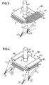
- FIG. 3 shows a highly simplified schematic representation of a placement head BK3, the suction pipette SP of which carries a component B.
- a spatially resolving optoelectronic transducer W3 is attached to the placement head BK3 in such a way that central projection from two different directions on its light-sensitive surface successively produces an immediate shadow of the connection area on one component side.
- the spatial position of the connections A can then be calculated from the different position of corresponding shadow edges of the connections A on the light-sensitive surface of the spatially resolving optoelectronic converter W3 by using the geometric radiation laws. This calculation will be explained in detail later with reference to FIGS. 7 and 8.
- the Calculation of the spatial position of the connections A then again includes position detection and a division and coplanarity check.
- the above-mentioned central projection from two different directions is brought about by two laser diodes LD1 and LD2 arranged at a distance from one another.
- These laser diodes LD1 and LD2 attached to the placement head BK3 are intended, as indicated by arrows S, to successively produce an immediate shadow cast of the connection area of a component side on the light-sensitive surface of the spatially resolving optoelectronic transducer W3. Since the laser diodes LD1 and LD2 are point light sources, there is a shadow cast by a central projection.
- Figure 4 shows a variant of the placement head shown in Figure 3.
- the placement head designated here with BK4 carries a spatially resolving optoelectronic converter W4 on opposite sides.
- the two spatially resolving optoelectronic transducers W4 are each separated by a direction perpendicular to their line direction, i. H. in the direction of the double arrows Pf2, movable photodiode array is formed.
- the two photodiode rows are each assigned two laser diodes LD1 and LD2 arranged at a distance from one another.
- the other two component sides for position detection and division and coplanarity check of the connections can also be detected by a single rotation D of the component B relative to the two spatially resolving optoelectronic transducers W4 by 90 °.
- FIGS. 5 and 6 show in a highly simplified schematic representation for the placement head BK4 shown in FIG. 4 the arrangement of photodiode lines and light sources during the inspection process and during the placement process. It can be seen that the spatially resolving optoelectronic transducers W4 and the two associated laser diodes LD1 and LD2, one behind the other perpendicular to the plane of the drawing, each have a common holder H are attached.
- the mutually opposite holders H can be moved with the aid of adjusting devices VE in the direction of the double arrows Pf2, that is to say during the test process the spatially resolving optoelectronic transducers W4 are moved synchronously with the associated laser diodes LD1 and LD2 relative to the connections A to be detected.
- the adjustment devices VE are attached to a longitudinal guide LF, in which the suction pipette SP can be raised and lowered in the direction of the double arrow Pf3 and rotatably in the direction of the double arrow D.
- This correction can include both a displacement and a rotation of the component B relative to the printed circuit board LP.
- FIGS. 7 and 8 show, for the placement head BK4 described above with reference to FIGS. 4, 5 and 6, the determination of the spatial position of the connections A of a component B.
- FIG. 7 shows the spatially resolving optoelectronic transducer W4 formed by a photodiode line, the component arranged directly below it B with the connections A and below it the two laser diodes LD1 and LD2 arranged at a distance from one another.
- the length of the photodiode row designated L in FIG. 8 is matched to the length of the component B.
- the distance between the underside of the photodiode array and the two laser diodes LD1 and LD2 is denoted by A '.
- a ' the distance between the laser diodes LD1 and LD2 and the left edge R in FIG. 7 of the photodiode line D1 and D2 is designated.
- the shadow edges of a specific connection A which are generated in succession by the radiation S from the laser diodes LD1 and LD2 on the photodiode array, are at a distance d1 or a distance d2 from the left edge R of the photodiode array in the horizontal direction.
- connection A The horizontal distance of this specific connection A from the left edge R is shown by the coordinate x, while in the vertical direction the distance of the connections A from the underside of the photodiode line is shown by the coordinate z.
- coordinate x By determining the coordinates x, a position detection and a division check of the connections A can be carried out, while the coordinates z of the connections A enable a coplanarity check.
- the converter W4 formed by a row of photodiodes has rectangular photodiodes FD and can be moved in the direction of the double arrows Pf2. This movability ensures a clear shadow cast by the connections A even when the component B is rotated.
- the method of the photodiode array also enables the twist of a component B to be determined, so that any twists during positioning on a printed circuit board can also be corrected.
- photodiode arrays from Reticon, Sunnyvale, California, USA with the designation RL 4096 N are used as the spatially resolving optoelectronic transducers.
- These photodiode rows each comprise 4096 individual photodiodes arranged in a row, the light-sensitive areas of the individual photodiodes having dimensions of 15 ⁇ 16 micrometers. The length of a row of photodiodes is 60 mm.
- Laser diodes from Hitachi Ltd, Tokyo, Japan with the designation HL 6711 C are used as punctiform light sources or laser diodes LD1 and LD2.
- These laser diodes have a power of 5 mW and emit light with a wavelength of 670 nm.
- the high number of individual photodiodes in a row of photodiodes ensures that at high resolution only the necessary information is recorded and read out in the shortest possible time, for example 2 ms can be.
Landscapes
- Engineering & Computer Science (AREA)
- Operations Research (AREA)
- Manufacturing & Machinery (AREA)
- Microelectronics & Electronic Packaging (AREA)
- Length Measuring Devices By Optical Means (AREA)
- Automatic Assembly (AREA)
Claims (20)
- Procédé de reconnaissance de la position et/ou de vérification de l'écartement et/ou de vérification de la coplanarité des raccordements (A) de composants (B), dans lequel, par un éclairage provenant de deux directions différentes, on produit successivement à la surface photosensible d'un convertisseur (W2; W3; W4) optoélectronique à définition spatiale des projections directes d'ombre de la zone de raccordement d'une face de composant et, à partir de la différence de position de bords d'ombre correspondants des raccordements (A) sur le convertisseur (W2; W3; W4) optoélectronique, on calcule la position dans l'espace du raccordement (A).
- Procédé de reconnaissance de la position et/ou de vérification de l'écartement et/ou de vérification de la coplanarité des raccordements (A) de composants (B), que, à l'aide d'une tête (BK2; BK3; BK4) d'insertion, on prélève d'une position de prélèvement prescrite d'un dispositif de mise à disposition de composants et qu'on met en position en une position prescrite sur une plaquette (LP) à circuits imprimés ou sur un substrat en céramique, caractérisé en ce que, par un éclairage provenant de deux directions différentes, on produit successivement à la surface photosensible d'un convertisseur (W2; W3; W4) optoélectronique à définition spatiale monté sur la tête (BK2;BK3;BK4) d'insertion des projections directes d'ombre de la zone de raccordement d'une face de composant et en ce que, à partir de la différence de position de bords d'ombre correspondants des raccordements (A) sur le convertisseur (W2; W3; W4) optoélectronique, on calcule la position dans l'espace du raccordement (A).
- Procédé suivant l'une des revendications 1 ou 2, caractérisé en ce que l'on utilise comme convertisseur (W1; W2; W3) optoélectronique à définition spatiale une photodiode (FD) pouvant être déplacée dans deux directions (Pf1, Pf2) perpendiculaires l'une à l'autre.
- Procédé suivant l'une des revendications 1 à 2, caractérisé en ce que l'on utilise comme convertisseur (W4) optoélectronique à définition spatiale une ligne de photodiode pouvant être déplacée perpendiculairement à la direction de la ligne.
- Procédé suivant la revendication 4, caractérisé en ce que l'on utilise une ligne de photodiodes dont les photodiodes (FD) individuelles comportent des surfaces photosensibles rectangulaires, s'étendant en long perpendiculairement à la direction de la ligne.
- Procédé suivant l'une des revendications 1 à 2, caractérisé en ce que l'on utilise comme convertisseur (W1; W2; W3) optoélectronique à définition spatiale une matrice de photodiodes.
- Procédé suivant l'une des revendications 1 à 6, caractérisé en ce que l'on utilise, pour l'éclairage provenant de deux directions différentes, au moins une source lumineuse ponctuelle.
- Procédé suivant la revendication 7, caractérisé en ce que l'on utilise, pour l'éclairage provenant de deux directions différentes, deux sources lumineuses ponctuelles disposées à distance l'une de l'autre.
- Procédé suivant la revendication 7 ou 8, caractérisé en ce que l'on utilise une diode (LD1, LD2) laser comme source lumineuse ponctuelle.
- Procédé suivant la revendication 2 et l'une des revendications 7 à 9, caractérisé en ce que l'on utilise, pour l'éclairage provenant de deux directions différentes, au moins une source lumineuse ponctuelle montée sur la tête (BK3; BK4) d'insertion.
- Procédé suivant les revendications 4 et 10, caractérisé en ce que l'on déplace la source lumineuse ponctuelle en synchronisme avec la ligne de photodiodes, perpendiculairement à la direction de cette ligne.
- Procédé suivant l'une des revendications précédentes, caractérisé en ce que, pour détecter toutes les zones de raccordement, on tourne le composant (B) associé par étapes de 90° ou de 180° par rapport au convertisseur (W1; W2; W3; W4) optoélectronique à définition spatiale.
- Procédé suivant la revendication 2 et suivant la revendication 12, caractérisé en ce que l'on tourne les composants (B) à l'aide de la pipette (SP) d'aspiration de la tête (BK1; BK2; BK3; BK4) d'insertion.
- Tête (BK4) d'insertion pour insérer automatiquement des composants (B) dans des plaquettes (LP) à circuits imprimés et dans des substrats en céramique, comportant- une pipette (SP) d'aspiration pour recevoir, transporter et mettre en position les composants,- un convertisseur (W4) optoélectronique à définition spatiale et- au moins une source lumineuse- la pipette (SP) d'aspiration, le convertisseur (W4) optoélectronique à définition spatiale et la source lumineuse étant disposés de telle manière que la source lumineuse, par un éclairage provenant de deux directions différentes, produit successivement à la surface photosensible du convertisseur (W4) optoélectronique à définition spatiale des projections directes d'ombre de la zone de raccordement d'une face d'un composant (B) reçu par la pipette (SP) d'aspiration et que, à partir de la différence de position de bords d'ombre correspondants des raccordements (A) du composant (B) sur le convertisseur (W4) optoélectronique, la position dans l'espace du raccordement (A) est calculée.
- Tête d'insertion suivant la revendication 14, caractérisée en ce que le convertisseur (W4) optoélectronique à définition spatiale est formé par une ligne de photodiode pouvant être déplacée perpendiculairement à la direction de la ligne.
- Tête d'insertion suivant la revendication 15, caractérisé en ce que les photodiodes (FD) individuelles de la ligne de photodiodes comportent des surfaces photosensibles rectangulaires, s'étendant en long perpendiculairement à la direction de la ligne.
- Tête d'insertion suivant l'une des revendications 14 à 16, caractérisée par une source lumineuse ponctuelle.
- Tête d'insertion suivant la revendication 17, caractérisée par deux sources lumineuses ponctuelles, disposées à distance l'une de l'autre.
- Tête d'insertion suivant la revendication 18, caractérisée par deux diodes (LD1, LD2) laser disposées à distance l'une de l'autre.
- Tête d'insertion suivant les revendications 15 et 18 ou 19, caractérisée en ce que les sources lumineuses ponctuelles peuvent, par l'intermédiaire d'une fixation (H) commune, être déplacées en synchronisme avec la ligne de photodiodes, perpendiculairement à la direction de la ligne.
Applications Claiming Priority (3)
| Application Number | Priority Date | Filing Date | Title |
|---|---|---|---|
| DE4209524A DE4209524A1 (de) | 1992-03-24 | 1992-03-24 | Verfahren zur Lageerkennung und/oder Teilungsprüfung und/oder Koplanaritätsprüfung der Anschlüsse von Bauelementen und Bestückkopf für die automatische Bestückung von Bauelementen |
| DE4209524 | 1992-03-24 | ||
| PCT/DE1993/000208 WO1993019577A1 (fr) | 1992-03-24 | 1993-03-08 | Procede d'identification de la position et/ou de controle de l'ecartement et/ou de controle de la coplanarite des raccordements de composants et tete pour l'implantation automatique de composants |
Publications (2)
| Publication Number | Publication Date |
|---|---|
| EP0632952A1 EP0632952A1 (fr) | 1995-01-11 |
| EP0632952B1 true EP0632952B1 (fr) | 1997-10-22 |
Family
ID=6454876
Family Applications (1)
| Application Number | Title | Priority Date | Filing Date |
|---|---|---|---|
| EP93905165A Expired - Lifetime EP0632952B1 (fr) | 1992-03-24 | 1993-03-08 | Procede d'identification de la position et/ou de controle de l'ecartement et/ou de controle de la coplanarite des raccordements de composants et tete pour l'implantation automatique de composants |
Country Status (5)
| Country | Link |
|---|---|
| US (2) | US5502890A (fr) |
| EP (1) | EP0632952B1 (fr) |
| AT (1) | ATE159641T1 (fr) |
| DE (2) | DE4209524A1 (fr) |
| WO (1) | WO1993019577A1 (fr) |
Families Citing this family (17)
| Publication number | Priority date | Publication date | Assignee | Title |
|---|---|---|---|---|
| DE4209524A1 (de) * | 1992-03-24 | 1993-09-30 | Siemens Ag | Verfahren zur Lageerkennung und/oder Teilungsprüfung und/oder Koplanaritätsprüfung der Anschlüsse von Bauelementen und Bestückkopf für die automatische Bestückung von Bauelementen |
| EP0808554A1 (fr) * | 1995-12-11 | 1997-11-26 | QTec Industrie-Automation GmbH | Procede et dispositif de mesure tridimensionnelle sans contact de la geometrie de fils de connexion dans des composants a semi-conducteurs |
| JPH09250393A (ja) * | 1996-01-12 | 1997-09-22 | Honda Motor Co Ltd | 往復型内燃機関におけるシリンダとシリンダヘッドとの密封構造およびその密封構造の組付け方法。 |
| AU4660496A (en) * | 1996-02-12 | 1997-09-02 | Icos Vision Systems N.V. | Process for forming on an opto-electronic transducer a shadow image of at least a part of an electronic component |
| US5739913A (en) * | 1996-08-02 | 1998-04-14 | Mrs Technology, Inc. | Non-contact edge detector |
| WO1998028953A2 (fr) * | 1996-12-20 | 1998-07-02 | Siemens Aktiengesellschaft | Procede pour determiner la position de connexions de composants electriques, notamment pour verifier la coplanarite dans des modules montes en surface |
| US6480223B1 (en) | 1997-09-30 | 2002-11-12 | Siemens Aktiengesellschaft | Method and device for detecting the position of terminals and/or edge of components |
| DE19823942C1 (de) * | 1998-05-28 | 1999-10-07 | Siemens Ag | Verfahren und Vorrichtung zur Schräglagenprüfung und/oder Koplanaritätsprüfung einer Kontaktreihe von SMD-Bauelementen |
| US6229608B1 (en) * | 1999-06-10 | 2001-05-08 | Pmj Automec Oyj | Procedure and system for inspecting a component with leads to determine its fitness for assembly |
| US20020173876A1 (en) * | 2000-12-15 | 2002-11-21 | Fisher Lance K. | Board align image acquisition device with improved interface |
| JP4278386B2 (ja) * | 2000-12-15 | 2009-06-10 | サイバーオプティクス コーポレーション | 改良された照明器を有するカメラ |
| US6762847B2 (en) | 2001-01-22 | 2004-07-13 | Cyberoptics Corporation | Laser align sensor with sequencing light sources |
| US6909515B2 (en) | 2001-01-22 | 2005-06-21 | Cyberoptics Corporation | Multiple source alignment sensor with improved optics |
| EP1391689A1 (fr) * | 2002-08-16 | 2004-02-25 | Komax Holding Ag | Dispositif et procédé pour détecter des garnitures |
| JP4046030B2 (ja) * | 2002-08-30 | 2008-02-13 | 株式会社村田製作所 | 部品装着方法および部品装着装置 |
| DE102005023705A1 (de) * | 2005-05-23 | 2006-11-30 | Siemens Ag | Sensor und Sensorsystem zur optischen Erfassung von Objekten, Bestückkopf, Verfahren zur Bestimmung der Höhenposition eines Bauelements |
| DE102007026900A1 (de) * | 2007-06-11 | 2008-12-18 | Siemens Ag | Auswerten der Oberflächenstruktur von Bauelementen unter Verwendung von unterschiedlichen Präsentationswinkeln |
Family Cites Families (25)
| Publication number | Priority date | Publication date | Assignee | Title |
|---|---|---|---|---|
| CH636740A5 (fr) * | 1980-05-19 | 1983-06-15 | Far Fab Assortiments Reunies | Dispositif pour l'alignement d'une piece et d'un substrat. |
| EP0144717B1 (fr) * | 1983-11-05 | 1988-10-19 | Zevatech AG | Procédé et dispositif de positionnement de composants sur une pièce à usiner |
| DE3340084C2 (de) * | 1983-11-05 | 1985-10-31 | Zevatech AG, Bellach | Vorrichtung zur Positionierung von Bauteilen auf einem Werkstück |
| SE8405803D0 (sv) * | 1984-11-19 | 1984-11-19 | Mydata Automation Ab | Anordning for centrering/uppmetning av komponenter |
| JPS61152100A (ja) * | 1984-12-26 | 1986-07-10 | ティーディーケイ株式会社 | 電子部品装着装置及びその方法 |
| JPH0797019B2 (ja) * | 1986-06-12 | 1995-10-18 | 松下電器産業株式会社 | 部品認識用照明方法及びその装置 |
| JPS6354000A (ja) * | 1986-08-22 | 1988-03-08 | 三洋電機株式会社 | 電子部品の位置検出装置 |
| JPS63168086A (ja) * | 1986-12-29 | 1988-07-12 | 株式会社東芝 | 電子部品の半田付け方法 |
| US4812666A (en) * | 1987-09-17 | 1989-03-14 | Universal Instruments Corporation | Position feedback enhancement over a limited repositioning area for a moveable member |
| GB8816730D0 (en) * | 1988-07-14 | 1988-08-17 | Pa Consulting Services | Improved vision system |
| US4951383A (en) * | 1988-11-14 | 1990-08-28 | Sanyo Electric Co., Ltd. | Electronic parts automatic mounting apparatus |
| EP0425722A1 (fr) * | 1989-10-31 | 1991-05-08 | Siemens Aktiengesellschaft | Dispositif de reconnaissance de position de pattes de connexion |
| GB9004246D0 (en) * | 1990-02-26 | 1990-04-18 | Automation Tooling Syst | Vision system for inspection of electronic components |
| US4980327A (en) * | 1990-03-06 | 1990-12-25 | United Catalysts Inc. | Reduced and stabilized hydrogenation catalysts |
| DE69116709T2 (de) * | 1990-03-19 | 1997-02-06 | Hitachi Ltd | Vorrichtung und Verfahren zum Transport von Bauteilen |
| BE1003136A3 (nl) * | 1990-03-23 | 1991-12-03 | Icos Vision Systems Nv | Werkwijze en inrichting voor het bepalen van een positie van ten minste een aansluitpen van een elektronische component. |
| US5044072A (en) * | 1990-04-13 | 1991-09-03 | Air-Vac Engineering Company, Inc. | Vision system apparatus and method for component/pad alignment |
| US5113565A (en) * | 1990-07-06 | 1992-05-19 | International Business Machines Corp. | Apparatus and method for inspection and alignment of semiconductor chips and conductive lead frames |
| US5251266A (en) * | 1990-08-27 | 1993-10-05 | Sierra Research And Technology, Inc. | System for placement and mounting of fine pitch integrated circuit devices using a split mirror assembly |
| US5249349A (en) * | 1991-01-24 | 1993-10-05 | Matsushita Electric Works, Ltd. | Parts mounting device |
| JPH04291795A (ja) * | 1991-03-20 | 1992-10-15 | Matsushita Electric Ind Co Ltd | 電子部品装着装置 |
| JPH05218693A (ja) * | 1992-01-23 | 1993-08-27 | Nec Corp | 電子部品搭載機 |
| DE4209524A1 (de) * | 1992-03-24 | 1993-09-30 | Siemens Ag | Verfahren zur Lageerkennung und/oder Teilungsprüfung und/oder Koplanaritätsprüfung der Anschlüsse von Bauelementen und Bestückkopf für die automatische Bestückung von Bauelementen |
| US5214841A (en) * | 1992-09-23 | 1993-06-01 | Emhart Inc. | Machine for placing surface mount components |
| JP3261770B2 (ja) * | 1992-11-19 | 2002-03-04 | 松下電器産業株式会社 | 部品装着装置 |
-
1992
- 1992-03-24 DE DE4209524A patent/DE4209524A1/de not_active Withdrawn
-
1993
- 1993-03-08 WO PCT/DE1993/000208 patent/WO1993019577A1/fr not_active Ceased
- 1993-03-08 DE DE59307577T patent/DE59307577D1/de not_active Expired - Fee Related
- 1993-03-08 AT AT93905165T patent/ATE159641T1/de not_active IP Right Cessation
- 1993-03-08 EP EP93905165A patent/EP0632952B1/fr not_active Expired - Lifetime
- 1993-03-08 US US08/307,749 patent/US5502890A/en not_active Expired - Lifetime
-
1996
- 1996-04-01 US US08/625,128 patent/US5687475A/en not_active Expired - Lifetime
Also Published As
| Publication number | Publication date |
|---|---|
| EP0632952A1 (fr) | 1995-01-11 |
| US5502890A (en) | 1996-04-02 |
| US5687475A (en) | 1997-11-18 |
| ATE159641T1 (de) | 1997-11-15 |
| DE59307577D1 (de) | 1997-11-27 |
| DE4209524A1 (de) | 1993-09-30 |
| WO1993019577A1 (fr) | 1993-09-30 |
Similar Documents
| Publication | Publication Date | Title |
|---|---|---|
| EP0632952B1 (fr) | Procede d'identification de la position et/ou de controle de l'ecartement et/ou de controle de la coplanarite des raccordements de composants et tete pour l'implantation automatique de composants | |
| DE69710714T2 (de) | Elektronische bauteile bestückungsvorrichtung | |
| EP2908614B9 (fr) | Mesure optique d'un composant présentant des caractéristiques structurales sur des côtés opposés | |
| DE3689406T2 (de) | Verfahren zur Plazierung eines oberflächenmontierten Teiles und eine Vorrichtung dazu. | |
| EP0023574B1 (fr) | Dispositif opto-électronique d'essai pour l'inspection automatique de la qualité de plaquettes à circuit imprimé, de leurs produits intermédiaires et des outils à imprimer | |
| CH643959A5 (de) | Verfahren und vorrichtung zur automatischen lageerkennung von halbleiterchips. | |
| DE102017202059A1 (de) | Platinenuntersuchungsvorrichtung | |
| EP0005462A2 (fr) | Procédé pour positionner deux objets à ajuster l'un sur l'autre | |
| WO2009033551A1 (fr) | Dispositif de navigation optique | |
| WO2008068136A1 (fr) | Procédé et dispositif pour mesurer une différence de hauteur | |
| DE102017203853A1 (de) | Platinenuntersuchungsvorrichtung | |
| DE10295831T5 (de) | Verbesserter Laserjustiersensor zum Positionieren von Komponenten | |
| EP0085868A1 (fr) | Dispositif de contrôle viruel de qualité automatique | |
| DE4139189C2 (de) | Vorrichtung zur optischen Lötstellenprüfung | |
| DE2944161C2 (de) | Vorrichtung zur Feststellung der Scharfeinstellung eines optischen Systems | |
| DE2822269C2 (de) | Verfahren zur automatischen Ausrichtung von zwei aufeinander einzujustierenden Objekten | |
| WO1995021376A1 (fr) | Dispositif d'imagerie destine a un objet tridimensionnel | |
| EP0399138A2 (fr) | Procédé pour l'examen en trois dimensions de circuits imprimés | |
| DE102008009680A1 (de) | Dreidimensionale Vermessung von Objekten mittels eines modular aufgebauten Triangulationssensors | |
| DE4308456C2 (de) | Vorrichtung zur Lagebestimmung eines Positionierkörpers relativ zu einem Bezugskörper | |
| DE3248382A1 (de) | Verfahren und vorrichtung zum ausrichten | |
| EP1020106B1 (fr) | Procede et dispositif pour la reconnaissance de la position de connexions et/ou de bords de composants | |
| DE69530099T2 (de) | Bauteile-bildwiedergabe | |
| DE19944721A1 (de) | Verfahren und Vorrichtung zum Ausrichten von Bauelementen | |
| DE3245315A1 (de) | Positioniervorrichtung fuer halbleiterchips |
Legal Events
| Date | Code | Title | Description |
|---|---|---|---|
| PUAI | Public reference made under article 153(3) epc to a published international application that has entered the european phase |
Free format text: ORIGINAL CODE: 0009012 |
|
| 17P | Request for examination filed |
Effective date: 19940915 |
|
| AK | Designated contracting states |
Kind code of ref document: A1 Designated state(s): AT BE CH DE FR GB IT LI NL |
|
| 17Q | First examination report despatched |
Effective date: 19951004 |
|
| GRAG | Despatch of communication of intention to grant |
Free format text: ORIGINAL CODE: EPIDOS AGRA |
|
| GRAH | Despatch of communication of intention to grant a patent |
Free format text: ORIGINAL CODE: EPIDOS IGRA |
|
| GRAH | Despatch of communication of intention to grant a patent |
Free format text: ORIGINAL CODE: EPIDOS IGRA |
|
| GRAA | (expected) grant |
Free format text: ORIGINAL CODE: 0009210 |
|
| AK | Designated contracting states |
Kind code of ref document: B1 Designated state(s): AT BE CH DE FR GB IT LI NL |
|
| REF | Corresponds to: |
Ref document number: 159641 Country of ref document: AT Date of ref document: 19971115 Kind code of ref document: T |
|
| REG | Reference to a national code |
Ref country code: CH Ref legal event code: NV Representative=s name: SIEMENS SCHWEIZ AG Ref country code: CH Ref legal event code: EP |
|
| REF | Corresponds to: |
Ref document number: 59307577 Country of ref document: DE Date of ref document: 19971127 |
|
| ET | Fr: translation filed | ||
| ITF | It: translation for a ep patent filed | ||
| GBT | Gb: translation of ep patent filed (gb section 77(6)(a)/1977) |
Effective date: 19971224 |
|
| PLBE | No opposition filed within time limit |
Free format text: ORIGINAL CODE: 0009261 |
|
| STAA | Information on the status of an ep patent application or granted ep patent |
Free format text: STATUS: NO OPPOSITION FILED WITHIN TIME LIMIT |
|
| 26N | No opposition filed | ||
| REG | Reference to a national code |
Ref country code: GB Ref legal event code: IF02 |
|
| PG25 | Lapsed in a contracting state [announced via postgrant information from national office to epo] |
Ref country code: FR Free format text: LAPSE BECAUSE OF NON-PAYMENT OF DUE FEES Effective date: 20031127 |
|
| REG | Reference to a national code |
Ref country code: FR Ref legal event code: ST |
|
| REG | Reference to a national code |
Ref country code: FR Ref legal event code: D3 |
|
| REG | Reference to a national code |
Ref country code: CH Ref legal event code: PCAR Free format text: SIEMENS SCHWEIZ AG;INTELLECTUAL PROPERTY FREILAGERSTRASSE 40;8047 ZUERICH (CH) |
|
| REG | Reference to a national code |
Ref country code: CH Ref legal event code: PUE Owner name: SIEMENS ELECTRONICS ASSEMBLY SYSTEMS GMBH & CO. K Free format text: SIEMENS AKTIENGESELLSCHAFT#WITTELSBACHERPLATZ 2#80333 MUENCHEN (DE) -TRANSFER TO- SIEMENS ELECTRONICS ASSEMBLY SYSTEMS GMBH & CO. KG#RUPERT-MAYER-STRASSE 44#81379 MUENCHEN (DE) |
|
| REG | Reference to a national code |
Ref country code: GB Ref legal event code: 732E Free format text: REGISTERED BETWEEN 20090903 AND 20090909 |
|
| NLS | Nl: assignments of ep-patents |
Owner name: SIEMENS ELECTRONICS ASSEMBLY SYSTEMS GMBH & CO. KG Effective date: 20090820 |
|
| PGFP | Annual fee paid to national office [announced via postgrant information from national office to epo] |
Ref country code: DE Payment date: 20090821 Year of fee payment: 17 Ref country code: CH Payment date: 20090811 Year of fee payment: 17 |
|
| REG | Reference to a national code |
Ref country code: FR Ref legal event code: TP |
|
| PGFP | Annual fee paid to national office [announced via postgrant information from national office to epo] |
Ref country code: IT Payment date: 20100324 Year of fee payment: 18 Ref country code: FR Payment date: 20100325 Year of fee payment: 18 |
|
| PGFP | Annual fee paid to national office [announced via postgrant information from national office to epo] |
Ref country code: GB Payment date: 20100311 Year of fee payment: 18 Ref country code: AT Payment date: 20100210 Year of fee payment: 18 |
|
| PGFP | Annual fee paid to national office [announced via postgrant information from national office to epo] |
Ref country code: NL Payment date: 20100303 Year of fee payment: 18 Ref country code: BE Payment date: 20100312 Year of fee payment: 18 |
|
| REG | Reference to a national code |
Ref country code: CH Ref legal event code: PL |
|
| PG25 | Lapsed in a contracting state [announced via postgrant information from national office to epo] |
Ref country code: LI Free format text: LAPSE BECAUSE OF NON-PAYMENT OF DUE FEES Effective date: 20100331 Ref country code: DE Free format text: LAPSE BECAUSE OF NON-PAYMENT OF DUE FEES Effective date: 20101001 Ref country code: CH Free format text: LAPSE BECAUSE OF NON-PAYMENT OF DUE FEES Effective date: 20100331 |
|
| BERE | Be: lapsed |
Owner name: SIEMENS ELECTRONICS ASSEMBLY SYSTEMS G.M.B.H. & CO Effective date: 20110331 |
|
| REG | Reference to a national code |
Ref country code: NL Ref legal event code: V1 Effective date: 20111001 |
|
| GBPC | Gb: european patent ceased through non-payment of renewal fee |
Effective date: 20110308 |
|
| PG25 | Lapsed in a contracting state [announced via postgrant information from national office to epo] |
Ref country code: AT Free format text: LAPSE BECAUSE OF NON-PAYMENT OF DUE FEES Effective date: 20110308 |
|
| REG | Reference to a national code |
Ref country code: FR Ref legal event code: ST Effective date: 20111130 |
|
| PG25 | Lapsed in a contracting state [announced via postgrant information from national office to epo] |
Ref country code: BE Free format text: LAPSE BECAUSE OF NON-PAYMENT OF DUE FEES Effective date: 20110331 |
|
| PG25 | Lapsed in a contracting state [announced via postgrant information from national office to epo] |
Ref country code: NL Free format text: LAPSE BECAUSE OF NON-PAYMENT OF DUE FEES Effective date: 20111001 |
|
| PG25 | Lapsed in a contracting state [announced via postgrant information from national office to epo] |
Ref country code: IT Free format text: LAPSE BECAUSE OF NON-PAYMENT OF DUE FEES Effective date: 20110308 Ref country code: GB Free format text: LAPSE BECAUSE OF NON-PAYMENT OF DUE FEES Effective date: 20110308 |
|
| PG25 | Lapsed in a contracting state [announced via postgrant information from national office to epo] |
Ref country code: FR Free format text: LAPSE BECAUSE OF NON-PAYMENT OF DUE FEES Effective date: 20110331 |