EP0634740B1 - Transducteur magnétorésistif de lecture - Google Patents
Transducteur magnétorésistif de lecture Download PDFInfo
- Publication number
- EP0634740B1 EP0634740B1 EP94304883A EP94304883A EP0634740B1 EP 0634740 B1 EP0634740 B1 EP 0634740B1 EP 94304883 A EP94304883 A EP 94304883A EP 94304883 A EP94304883 A EP 94304883A EP 0634740 B1 EP0634740 B1 EP 0634740B1
- Authority
- EP
- European Patent Office
- Prior art keywords
- layer
- transducer
- magnetoresistive
- magnetic
- active region
- Prior art date
- Legal status (The legal status is an assumption and is not a legal conclusion. Google has not performed a legal analysis and makes no representation as to the accuracy of the status listed.)
- Expired - Lifetime
Links
- 230000005291 magnetic effect Effects 0.000 claims description 67
- 238000000034 method Methods 0.000 claims description 32
- 239000003302 ferromagnetic material Substances 0.000 claims description 25
- 238000003860 storage Methods 0.000 claims description 19
- 239000002885 antiferromagnetic material Substances 0.000 claims description 15
- 239000000463 material Substances 0.000 claims description 14
- 238000000151 deposition Methods 0.000 claims description 13
- 239000000696 magnetic material Substances 0.000 claims description 12
- 239000000758 substrate Substances 0.000 claims description 10
- 230000005290 antiferromagnetic effect Effects 0.000 claims description 8
- 238000005530 etching Methods 0.000 claims description 6
- 229910045601 alloy Inorganic materials 0.000 claims description 4
- 239000000956 alloy Substances 0.000 claims description 4
- UGKDIUIOSMUOAW-UHFFFAOYSA-N iron nickel Chemical compound [Fe].[Ni] UGKDIUIOSMUOAW-UHFFFAOYSA-N 0.000 claims description 4
- 238000004519 manufacturing process Methods 0.000 claims description 3
- 238000003801 milling Methods 0.000 claims description 3
- 229920002120 photoresistant polymer Polymers 0.000 claims description 3
- 238000001514 detection method Methods 0.000 claims description 2
- 238000003384 imaging method Methods 0.000 claims description 2
- ZAUUZASCMSWKGX-UHFFFAOYSA-N manganese nickel Chemical compound [Mn].[Ni] ZAUUZASCMSWKGX-UHFFFAOYSA-N 0.000 claims description 2
- QKGPHOLBTUQGIA-UHFFFAOYSA-N [Rh].[Fe].[Ni] Chemical compound [Rh].[Fe].[Ni] QKGPHOLBTUQGIA-UHFFFAOYSA-N 0.000 claims 1
- 238000010884 ion-beam technique Methods 0.000 claims 1
- DALUDRGQOYMVLD-UHFFFAOYSA-N iron manganese Chemical compound [Mn].[Fe] DALUDRGQOYMVLD-UHFFFAOYSA-N 0.000 claims 1
- 239000010410 layer Substances 0.000 description 103
- 230000005294 ferromagnetic effect Effects 0.000 description 11
- 230000008569 process Effects 0.000 description 10
- 239000004020 conductor Substances 0.000 description 8
- 125000006850 spacer group Chemical group 0.000 description 8
- 229910001030 Iron–nickel alloy Inorganic materials 0.000 description 6
- 230000008878 coupling Effects 0.000 description 6
- 238000010168 coupling process Methods 0.000 description 6
- 238000005859 coupling reaction Methods 0.000 description 6
- 230000005415 magnetization Effects 0.000 description 5
- 230000008021 deposition Effects 0.000 description 3
- 238000010586 diagram Methods 0.000 description 3
- 239000002356 single layer Substances 0.000 description 3
- 238000000992 sputter etching Methods 0.000 description 3
- 239000000725 suspension Substances 0.000 description 3
- 229910016897 MnNi Inorganic materials 0.000 description 2
- 230000005316 antiferromagnetic exchange Effects 0.000 description 2
- 230000015572 biosynthetic process Effects 0.000 description 2
- GUBSQCSIIDQXLB-UHFFFAOYSA-N cobalt platinum Chemical compound [Co].[Pt].[Pt].[Pt] GUBSQCSIIDQXLB-UHFFFAOYSA-N 0.000 description 2
- 239000010931 gold Substances 0.000 description 2
- 230000004044 response Effects 0.000 description 2
- 229910052715 tantalum Inorganic materials 0.000 description 2
- GUVRBAGPIYLISA-UHFFFAOYSA-N tantalum atom Chemical compound [Ta] GUVRBAGPIYLISA-UHFFFAOYSA-N 0.000 description 2
- 230000005330 Barkhausen effect Effects 0.000 description 1
- DTJAVSFDAWLDHQ-UHFFFAOYSA-N [Cr].[Co].[Pt] Chemical compound [Cr].[Co].[Pt] DTJAVSFDAWLDHQ-UHFFFAOYSA-N 0.000 description 1
- 230000008859 change Effects 0.000 description 1
- 238000003486 chemical etching Methods 0.000 description 1
- 229910017052 cobalt Inorganic materials 0.000 description 1
- 239000010941 cobalt Substances 0.000 description 1
- GUTLYIVDDKVIGB-UHFFFAOYSA-N cobalt atom Chemical compound [Co] GUTLYIVDDKVIGB-UHFFFAOYSA-N 0.000 description 1
- 239000010952 cobalt-chrome Substances 0.000 description 1
- 230000003247 decreasing effect Effects 0.000 description 1
- 238000004090 dissolution Methods 0.000 description 1
- 230000005284 excitation Effects 0.000 description 1
- 239000010408 film Substances 0.000 description 1
- PCHJSUWPFVWCPO-UHFFFAOYSA-N gold Chemical compound [Au] PCHJSUWPFVWCPO-UHFFFAOYSA-N 0.000 description 1
- 229910052737 gold Inorganic materials 0.000 description 1
- 238000000059 patterning Methods 0.000 description 1
- 238000000206 photolithography Methods 0.000 description 1
- 238000004544 sputter deposition Methods 0.000 description 1
- 230000001629 suppression Effects 0.000 description 1
- 239000010409 thin film Substances 0.000 description 1
- 238000012876 topography Methods 0.000 description 1
- WFKWXMTUELFFGS-UHFFFAOYSA-N tungsten Chemical compound [W] WFKWXMTUELFFGS-UHFFFAOYSA-N 0.000 description 1
- 229910052721 tungsten Inorganic materials 0.000 description 1
- 239000010937 tungsten Substances 0.000 description 1
Images


Classifications
-
- G—PHYSICS
- G11—INFORMATION STORAGE
- G11B—INFORMATION STORAGE BASED ON RELATIVE MOVEMENT BETWEEN RECORD CARRIER AND TRANSDUCER
- G11B5/00—Recording by magnetisation or demagnetisation of a record carrier; Reproducing by magnetic means; Record carriers therefor
- G11B5/127—Structure or manufacture of heads, e.g. inductive
- G11B5/33—Structure or manufacture of flux-sensitive heads, i.e. for reproduction only; Combination of such heads with means for recording or erasing only
- G11B5/39—Structure or manufacture of flux-sensitive heads, i.e. for reproduction only; Combination of such heads with means for recording or erasing only using magneto-resistive devices or effects
- G11B5/3903—Structure or manufacture of flux-sensitive heads, i.e. for reproduction only; Combination of such heads with means for recording or erasing only using magneto-resistive devices or effects using magnetic thin film layers or their effects, the films being part of integrated structures
- G11B5/399—Structure or manufacture of flux-sensitive heads, i.e. for reproduction only; Combination of such heads with means for recording or erasing only using magneto-resistive devices or effects using magnetic thin film layers or their effects, the films being part of integrated structures with intrinsic biasing, e.g. provided by equipotential strips
-
- G—PHYSICS
- G11—INFORMATION STORAGE
- G11B—INFORMATION STORAGE BASED ON RELATIVE MOVEMENT BETWEEN RECORD CARRIER AND TRANSDUCER
- G11B5/00—Recording by magnetisation or demagnetisation of a record carrier; Reproducing by magnetic means; Record carriers therefor
- G11B5/127—Structure or manufacture of heads, e.g. inductive
Definitions
- the present invention relates generally to thin film magnetic transducers and, more particularly, to magnetic transducers having a magnetoresistive read transducer arranged such that a longitudinal bias field is produced in end regions of the transducer.
- 4,639,806 discloses an MR sensor which provides a longitudinal bias field produced by ferromagnetic exchange coupling between the MR layer and hard magnetic layers in the sensor end regions only.
- Commonly assigned U.S. Patent No. 5,079,035 discloses an MR sensor in which the ferromagnetic MR element extends over only the central active region of the sensor.
- a layer of hard magnetic material is provided in each of the sensor end regions which form an abutting junction with the ends of the HR element to provide a longitudinal magnetic bias field in the sensor.
- the central active region includes the MR element, a non-magnetic spacer layer and an adjacent soft magnetic layer which provides a transverse magnetic bias field for the sensor.
- the MR sensor design described in patent no. 5,079,035 has been shown to meet present requirements and provides numerous advantages, including data track definition by a single photolithography process step, controllable and reproducible etch stop of the sensor active region trilayer etch process, easily adjustable longitudinal bias field, and substantially no side reading.
- the contiguous or abutting junction hard bias design suffers from a substantial disadvantage which, while at large data track widths where the length of the sensor active region is large compared to the length of the junction region may not be discernible, at relatively small data track widths where the length of the active region can become comparable or even small compared to the length of the junction region, can cause the magnetic properties in the junction region to no longer be predictable or well-defined.
- European Patent Application 0 558 237 discloses a magnetoresistive read transducer and a method of manufacture of a magnetoresistive read transducer.
- the abutting junction between the end regions and the central regions forms a straight edge, that is, the magnetoresistive element and the bias layer do not overlap.
- the present invention provides a method for manufacturing a magnetoresistive read transducer having end regions separated by a central active region, the method comprising the steps of: depositing on a substrate a magnetoresistive layer of ferromagnetic material over at least the central active region of said transducer; forming a stencil covering said central active region of said transducer; etching away the portion of said magnetoresistive layer not covered by said stencil to form a magnetoresistive element extending over said central active region of said transducer; depositing a second layer of ferromagnetic material over regions of said transducer not covered by said stencil; and depositing a layer of antiferromagnetic material over regions of said transducer not covered by said stencil, said layer of antiferromagnetic material overlaying and being in contact with said second layer of ferromagnetic material, said layers of antiferromagnetic and ferromagnetic material forming an exchange-coupled bias layer extending over said end regions of said transducer; removing said stencil covering said central active region; said central
- the invention also provides a magnetoresistive read transducer having end regions separated by a central active region, the transducer comprising a magnetoresistive layer of ferromagnetic material extending over substantially only said central active region; a second layer of ferromagnetic material extending over substantially only said end regions of said transducer; and a layer of antiferromagnetic material overlaying and in contact with said second layer of ferromagnetic material, said layers of antiferromagnetic and ferromagnetic material forming an exchange-coupled bias layer extending over said end regions of said transducer; said exchange-coupled bias layer in each of said end regions forming an abutting junction with one end of said magnetoresistive layer, and producing a longitudinal magnetic bias field in said transducer; and wherein said abutting junction comprises overlapping tapered portions of said magnetoresistive layer and said bias layer.
- the invention further provides a magnetic storage system comprising: a magnetic storage medium having a plurality of tracks for recording of data; a magnetoresistive read transducer maintained in a closely spaced position relative to said magnetic storage medium during relative motion between said magnetoresistive read transducer and said magnetic storage medium; actuator means coupled to said magnetoresistive read transducer for moving said magnetoresistive read transducer to selected tracks on said magnetic storage medium; and detection means coupled to said magnetoresistive read transducer for detecting resistance changes in the magnetoresistive material responsive to magnetic fields representative of data bits recorded in said magnetic storage medium intercepted by said magnetoresistive transducer; wherein the magnetoresistive read transducer is a transducer as described above.
- FIG. 1 Although the invention is described as embodied in a magnetic disk storage system as shown in Fig. 1, it will be apparent that the invention is also applicable to other magnetic recording systems such as a magnetic tape recording system, for example.
- At least one rotatable magnetic disk 12 is supported on a spindle 14 and rotated by a disk drive motor 18.
- the magnetic recording media on each disk is in the form of an annular pattern of concentric data tracks (not shown) on disk 12.
- At least one slider 13 is positioned on the disk 12, each slider 13 supporting one or more magnetic read/write transducers 21, typically referred to as read/write heads. As the disks rotate, the sliders 13 are moved radially in and out over the disk surface 22 so that the heads 21 may access different portions of the disk where desired data is recorded.
- Each slider 13 is attached to an actuator arm 19 by means of a suspension 15.
- the suspension 15 provides a slight spring force which biases the slider 13 against the disk surface 22.
- Each actuator arm 19 is attached to an actuator means 27.
- the actuator means as shown in Fig.1 may be a voice coil motor (VCM), for example.
- the VCM comprises a coil moveable within a fixed magnetic field, the direction and velocity of the coil movements being controlled by the motor current signals supplied by a controller.
- the rotation of the disk 12 generates an air bearing between the slider 13 and the disk surface 22 which exerts an upward force or lift on the slider.
- the air bearing thus counterbalances the slight spring force of the suspension 15 and supports the slider 13 off and slightly above the disk surface by a small, substantially constant spacing during operation.
- control unit 29 The various components of the disk storage system are controlled in operation by control signals generated by control unit 29, such as access control signals and internal clock signals.
- control unit 29 comprises logic control circuits, storage means and a microprocessor, for example.
- the control unit 29 generates control signals to control various system operations such as drive motor control signals on line 23 and head position and seek control signals on line 28.
- the control signals on line 28 provide the desired current profiles to optimally move and position a selected slider 13 to the desired data track on the associated disk 12.
- Read and write signals are communicated to and from read/write heads 21 by means of recording channel 25.
- disk storage systems may contain a large number of disks and actuators, and each actuator may support a number of sliders.
- a prior art MR read transducer of the type described in commonly assigned U.S. Patent No. 4,663,685 comprises an MR layer 32 which extends over the entire transducer 30'.
- a longitudinal bias layer 43 extends over the transducer end regions 36 only to produce a longitudinal bias field in the transducer.
- the read signal is sensed over the central active region 44 which is defined in transducer 30' by the spacing between lead conductors 46 deposited over the longitudinal bias layer 43.
- the MR read transducer 30 comprises a layer of ferromagnetic material forming an MR element 31 which extends over substantially only a central active region 33 of the transducer and a magnetic bias layer 35 formed in each end region 37 which forms an abutting junction 39 with the MR element 31 to produce a longitudinal magnetic bias field in the MR read transducer 30. Since the MR element 31 extends only over the central active region 33 of the transducer 30, additional side-reading suppression components are not required in this preferred embodiment. Thus, the longitudinal bias layer 35 in each end region 37 need only provide for electrical and magnetic continuity to the MR element 31.
- the longitudinal bias layer 35 may be a single layer of magnetically hard material such as cobalt-chromium (CoCr), cobalt-platinum (CoPt) or cobalt-chromium-platinum (CoCrPt), for example, although the use of under- and/or overcoats such as tungsten (W) or gold (Au) may be desirable.
- the longitudinal bias field can be provided by ferromagnetic/antiferromagnetic exchange coupling wherein the longitudinal bias layer 35 comprises a layer 75 of antiferromagnetic material overlaying and in physical contact with a layer 79 of ferromagnetic material (as shown in Fig. 7).
- the longitudinal bias layer 35 can comprise a bilayer of manganeseiron/nickel-iron (MnFe/NiFe) or a bilayer of manganese-nickel/nickel-iron (MnNi/NiFe).
- a transverse magnetic bias field is also required in the central active region 33.
- the transverse bias field can be provided by an adjacent soft magnetic layer, shunt bias, or other compatible transverse bias techniques.
- the transverse bias structure has not been shown in the conceptual view of Fig. 3.
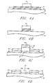
- a preferred embodiment of a process for fabricating a suitable abutting or contiguous junction between the MR element 31 and the longitudinal bias layer 35 is illustrated.
- the process according to the preferred embodiment of the present invention comprises the steps of depositing, upon a suitable substrate 40, an MR layer of ferromagnetic material such as NiFe, for example, over the length of the transducer.
- a transverse bias structure comprising a soft magnetic layer 43 and a non-magnetic spacer layer 45 are deposited on substrate 40 prior to depositing of the MR layer 31.
- the process then continues by depositing a layer of a suitable material such as a photoresist, and patterning the photoresist material to form a stencil 41 (Fig. 4a).
- Stencil 41 is used to define each edge of the MR layer 31 as the layer of MR material 31 as well as the spacer layer 45 and the soft magnetic layer 43 are subjected to a subtractive process such as sputter etching, ion milling or chemical etching to produce an MR trilayer structure 47 (Fig. 4b).
- the material for the longitudinal bias layers 35 is then deposited as stencil 41 again defines the edges of the bias layers 35 (Fig. 4c).
- a layer of conductive material is then deposited to produce the sensor conductor leads 49.
- conductor leads 49 can be deposited in a later step if the conductor leads 49 are not coextensive with the longitudinal bias layers 35.
- a quantity of magnetic material and lead material is also deposited on the top surface of stencil 41. However, this quantity of material is removed, along with stencil 41 in a lift-off process (Fig. 4d) as is known in the art to produce an MR sensor or transducer having longitudinal bias layers 35 in the end regions only, each having a contiguous, abutting junction with the MR trilayer structure 47 which extends over only the central active region 33.
- the preferred embodiments comprise a junction in which the topography is well-controlled so that a desired junction configuration can be easily and reliably produced.
- the stencil 41 comprises a bi-layer resist formed by a relatively thin underlayer 54 and a thick imaging layer 53.
- One exposure and one develop step defines the edge profile of the resist.
- An undercut 51 is created by dissolution of the underlayer 54 in a suitable developer with the undercut distance determined by the develop time.
- the unmasked areas of the layer 55 of MR material are then removed by the use of a unidirectional process such as ion milling, for example.
- the angle of incidence ⁇ is controlled by suitably tilting the substrate relative to the incident beam.
- circular symmetry is obtained by rotating the substrate so that any given point sees the incident beam rotate conically about the azimuth angle ⁇ except near the stencil 41 whose edge shadows the layer 55 during some segment of substrate revolution.
- Fig. 5 for an azimuth angle of 0 degrees, there is exposure of the layer 55 to point c and the exposure limit point moves progressively to the left until at an azimuth angle of 180 degrees the exposure limit point is moved to point a.
- the combined milling for this embodiment produces a curved taper 56 as a result of the removal during the milling process of the portion 57 of the layer 55 shown in the dashed lines.
- the longitudinal bias layer 58 is then deposited, by sputter deposition, for example, during a similar orientation and rotation of the substrate to produce a deposition profile such as that shown by dashed lines 59.
- the combined junction profile resulting from the deposition of bias layer 58 is shown in full line.
- conductor leads 73 (as shown in Fig. 7) can also be deposited in this sequence of steps.
- the longitudinal bias layer 58 is shown as a single layer in Fig. 5, it will be recognized that the longitudinal bias layer may comprise multilayers, such as a layer of ferromagnetic material overlaid by a layer of antiferromagnetic material to provide a longitudinal bias field by ferromagnetic/antiferromagnetic exchange coupling, for example.
- the MR layer 55 may comprise multiple layers, such as the MR trilayer 47 forming a transverse bias structure, for example.
- the junction profile 62 comprises two overlapping tapers.
- the taper profile is determined by the height of the stencil 41 and the selected angle of incidence ⁇ .
- the length of the junction overlap ⁇ should be relatively long; however, for magnetic reliability the length of the junction overlap ⁇ should be relatively short.
- the selected length of the junction overlap is a trade off in which typically the magnetic reliability is more heavily weighted than the electrical reliability.
- overmilling at low angles of incidence ⁇ prior to deposition of the bias layer 58 may be required.
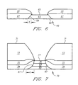
- a cross-sectional view of a preferred embodiment of an MR read transducer fabricated by the above-described method is shown, the surface of which is in close proximity to a magnetic recording medium from which previously recorded magnetic data is to be read.
- the transducer 60 comprises an MR element 63 which extends over the central active region 65 of the transducer, and hard magnetic bias layers 67 which form abutting junction 69 with the MR element 63.
- the hard magnetic bias layers 67 extend over the end regions 61 of the transducer to produce a longitudinal magnetic bias field in the MR element 63.
- the MR element 63 can comprise a trilayer structure including a layer of ferromagnetic material, such as NiFe, for example, a spacer layer of a nonmagnetic material, such as tantalum (Ta), for example, and a layer of soft magnetic material, such as NiFeRh, for example.
- the soft magnetic layer is separated from the MR layer by the spacer layer and provides the transverse bias field for the MR element 63.
- the hard magnetic bias layers 67 comprise a single layer of a hard magnetic material, such as CoCrPt, for example.
- the stencil 41 height was about 1 ⁇ m and the angle of incidence ⁇ was about 10 degrees with an overmill of 5 percent.
- This selected combination produced a junction length ⁇ of less than 0.1 ⁇ m.
- junction lengths within the range of 0 ⁇ ⁇ ⁇ 0.1 ⁇ m are suitable for use with transducers utilizing hard magnetic bias layers to produce the longitudinal bias field.
- the undercut 51 of stencil 41 (as shown in Fig. 5) can be adjusted to provide some overlap 64 of the conductor leads 68 with the MR element 63.
- the MR transducer 70 comprises a multilayer MR element which extends over the central active region 77 of the transducer, and a bilayer exchange coupled bias layer 75/79 deposited in each end region 71 which form abutting junctions 87 with the MR element.
- the bias layers 75/79 extend over the end regions 71 of the transducer to produce a longitudinal magnetic bias field in the MR element.
- the bias layers comprise a layer 75 of antiferromagnetic material, such as MnFe or MnNi, for example, overlaying and in contact with a layer 79 of a ferromagnetic material, such as NiFe, for example.
- the MR element comprises a trilayer structure including a layer 81 of ferromagnetic material, such as NiFe, for example, a spacer layer 83 of a nonmagnetic material, such as tantalum (Ta), for example, and a layer 85 of soft magnetic material, such as NiFeRh, for example.
- the soft magnetic layer 85 is separated from the MR layer 81 by the spacer layer 83 and provides the transverse bias field for the MR element.
- the magnetization in a ferromagnetic layer exchange-coupled to an antiferromagnetic layer will not change irreversibly, and thus will not cause any hysteric response with application of a transverse magnetic bias field.
- the magnetization in a ferromagnetic/antiferromagnetic couple will not vary with the substrate on which it is grown, and thus will not diminish when grown on the overlap region ⁇ of the junction 87.
- the stencil 41 height was about 1 ⁇ m and the angle of incidence ⁇ was in the range of about 70 to 80 degrees.
- This selected combination produced a junction length ⁇ of about 5 times the thickness of the MR element.
- junction lengths ⁇ within the range of 3 to 5 times the MR element thickness are suitable for use with transducers utilizing antiferromagnetic/ferromagnetic exchange-coupled bias layers to produce the longitudinal bias field.
- conductor leads 71 can be deposited in the same sequence of process steps and the MR element and the bias layers, or alternatively, can be deposited in subsequent steps.
Landscapes
- Engineering & Computer Science (AREA)
- Manufacturing & Machinery (AREA)
- Magnetic Heads (AREA)
- Hall/Mr Elements (AREA)
Claims (18)
- Un procédé de fabrication d'un transducteur de lecture magnétorésistif (30) ayant des zones d'extrémité (37) séparées par une zone active centrale (33), le procédé comprenant les étapes consistant à :déposer sur un substrat (40) une couche magnétorésistive de matériau ferromagnétique (31), sur au moins la zone centrale active dudit transducteur ;former un cliché-pochoir (41) couvrant ladite zone active centrale dudit transducteur ;éliminer par morsure la partie de ladite couche magnétorésistive non couverte par ledit cliché-pochoir, pour former un élément magnétorésistif s'étendant sur ladite zone active centrale dudit transducteur ;déposer une deuxième couche (79) de matériau ferromagnétique sur des zones dudit transducteur non couvertes par ledit cliché-pochoir ; etdéposer une couche de matériau antiferromagnétique (75) sur des zones dudit transducteur non couvertes par ledit cliché-pochoir, ladite couche de matériau antiferromagnétique recouvrant et étant mise en contact avec ladite deuxième couche de matériau ferromagnétique, lesdites couches de matériau antiferromagnétique et ferromagnétique formant une couche de polarisation, couplée en échange, s'étendant sur lesdites zones d'extrémité dudit transducteur ;éliminer ledit cliché-pochoir (41) couvrant ladite zone active centrale,ladite couche de polarisation couplée en échange se trouvant dans chacune desdites zones d'extrémité formant une jonction d'about (87) avec une extrémité dudit élément magnétorésistif, et produisant un champ de polarisation magnétique longitudinal dans ledit transducteur ; etdans lequel ladite jonction d'about est constituée de parties effilées, se chevauchant, dudit élément magnétorésistif et de ladite couche de polarisation.
- Un procédé selon la revendication 1, dans lequel la longueur de ladite jonction à chevauchement (87) est dans la plage d'environ trois à cinq fois l'épaisseur dudit élément magnétorésistif.
- Un procédé selon l'une quelconque des revendications 1 à 2, dans lequel ladite étape de morsure comprend l'utilisation d'un procédé de morsure directionnel.
- Un procédé selon la revendication 3, dans lequel ledit procédé de morsure directionnel comprend un fraisage par faisceau d'ions.
- Un procédé selon la revendication 3 ou la revendication 4, dans lequel ledit procédé de morsure directionnel est mis en oeuvre sous un certain angle par rapport audit transducteur (30).
- Un procédé selon la revendication 5, dans lequel ledit angle est situé dans la plage d'environ soixante-dix à quatre-vingt degrés.
- Un procédé selon la revendication 5 ou la revendication 6, dans lequel ledit transducteur (30) est tourné dans un plan perpendiculaire par rapport audit angle, durant ladite étape de morsure.
- Un procédé selon l'une quelconque des revendications précédentes, dans lequel ledit cliché-pochoir (41) est constitué d'un matériau photoresist ayant une sous-couche (54) mince et une couche d'imagerie (53) épaisse, recouvrant ladite sous-couche mince.
- Un procédé selon la revendication 8, dans lequel ladite sous-couche (54) est dotée d'une contre-dépouille.
- Un procédé selon l'une quelconque des revendications précédentes, comprenant en outre l'étape consistant à déposer une couche d'un matériau magnétiquement doux (85), espacée dudit élément magnétorésistif, pour produire un champ de polarisation magnétique transversal en au moins une partie de ladite zone active centrale (33).
- Un transducteur de lecture magnétorésistif (30) ayant des zones d'extrémité (37) séparées par une zone active centrale (33), le transducteur comprenant une couche magnétorésistive (31) en matériau ferromagnétique s'étendant sur sensiblement seulement ladite zone active centrale ;une deuxième couche (79) en matériau ferromagnétique s'étendant sur sensiblement seulement lesdites zones d'extrémité dudit transducteur ; etune couche de matériau antiferromagnétique (75) recouvrant et mise en contact avec ladite deuxième couche de matériau ferromagnétique, lesdites couches de matériau antiferromagnétique et ferromagnétique formant une couche de polarisation à échange de couplage, sur lesdites zones d'extrémité dudit transducteur ;ladite couche de polarisation à échange de couplage, dans chacune desdites zones d'extrémité, formant une jonction d'about (87) avec une extrémité de ladite couche magnétorésistive, et produisant un champ de polarisation magnétique longitudinal dans ledit transducteur ; etladite jonction d'about comprenant des zones effilées se chevauchant de ladite couche magnétorésistive et de ladite couche de polarisation.
- Un transducteur de lecture magnétorésistif (30) selon la revendication 11, dans lequel la longueur de ladite jonction à chevauchement (87) se trouve dans la plage d'environ trois à cinq fois l'épaisseur de ladite couche magnétorésistive.
- Un transducteur de lecture magnétorésistif (30) selon la revendication 11 ou la revendication 12, dans lequel lesdites parties effilées se chevauchant comprennent une surface incurvée continue.
- Un transducteur de lecture magnétorésistif (30) selon l'une quelconque des revendications 11 à 13, dans lequel ladite couche magnétorésistive est constituée d'un alliage de nickel-fer.
- Un transducteur de lecture magnétorésistif (30) selon l'une quelconque des revendications 11 à 14, dans lequel ledit matériau antiferromagnétique (75) est sélectionné dans le groupe constitué des alliages manganèse-fer et manganèse-nickel, et ledit matériau ferromagnétique (79) est constitué de nickel-fer.
- Un transducteur de lecture magnétorésistif (30) selon l'une quelconque des revendications 11 à 15, comprenant en outre une couche de matériau magnétiquement doux (85) espacée de ladite couche magnétorésistive, pour produire un champ de polarisation magnétique transversal en au moins une partie de ladite zone active centrale (33).
- Un transducteur de lecture magnétorésistif (30) selon la revendication 16, dans lequel ledit matériau magnétiquement doux (85) est constitué d'un alliage nickel-fer-rhodium.
- Un système de stockage magnétique comprenant :un milieu de stockage magnétique (12) ayant une pluralité de pistes destinées à enregistrer des données ;un transducteur de lecture magnétorésistif (30), maintenu en une position espacée intimement par rapport audit milieu de stockage magnétique, durant le déplacement relatif entre ledit transducteur de lecture magnétorésistif et ledit milieu de stockage magnétique ;des moyens actionneurs (19) couplés audit transducteur de lecture magnétorésistif, pour déplacer ledit transducteur de lecture magnétorésistif sur des pistes sélectionnées se trouvant sur ledit milieu de stockage magnétique ; etdes moyens de détection (25) couplés audit transducteur de lecture magnétorésistif, pour détecter des fluctuations de résistance se manifestant dans le matériau magnétorésistif, en réponse à des champs magnétiques représentatifs de bits de données enregistrés dans ledit milieu de stockage magnétique, interceptés par ledit transducteur magnétorésistif ;dans lequel le transducteur de lecture magnétorésistif est un transducteur tel qu'indiqué selon l'une quelconque des revendications 11 à 17.
Applications Claiming Priority (2)
| Application Number | Priority Date | Filing Date | Title |
|---|---|---|---|
| US9071493A | 1993-07-13 | 1993-07-13 | |
| US90714 | 1993-07-13 |
Publications (3)
| Publication Number | Publication Date |
|---|---|
| EP0634740A2 EP0634740A2 (fr) | 1995-01-18 |
| EP0634740A3 EP0634740A3 (fr) | 1996-01-31 |
| EP0634740B1 true EP0634740B1 (fr) | 1999-09-22 |
Family
ID=22223964
Family Applications (1)
| Application Number | Title | Priority Date | Filing Date |
|---|---|---|---|
| EP94304883A Expired - Lifetime EP0634740B1 (fr) | 1993-07-13 | 1994-07-04 | Transducteur magnétorésistif de lecture |
Country Status (8)
| Country | Link |
|---|---|
| EP (1) | EP0634740B1 (fr) |
| JP (1) | JP2710210B2 (fr) |
| KR (1) | KR0133248B1 (fr) |
| CN (1) | CN1064162C (fr) |
| DE (1) | DE69420789T2 (fr) |
| MY (1) | MY121197A (fr) |
| SG (1) | SG44410A1 (fr) |
| TW (1) | TW428779U (fr) |
Families Citing this family (22)
| Publication number | Priority date | Publication date | Assignee | Title |
|---|---|---|---|---|
| US5438470A (en) * | 1994-05-13 | 1995-08-01 | Read-Rite Corporation | Magnetoresistive structure with contiguous junction hard bias design with low lead resistance |
| US5528440A (en) | 1994-07-26 | 1996-06-18 | International Business Machines Corporation | Spin valve magnetoresistive element with longitudinal exchange biasing of end regions abutting the free layer, and magnetic recording system using the element |
| JPH0887721A (ja) * | 1994-09-16 | 1996-04-02 | Tdk Corp | 磁気変換素子及び薄膜磁気ヘッド |
| US5434826A (en) * | 1994-09-26 | 1995-07-18 | Read-Rite Corporation | Multilayer hard bias films for longitudinal biasing in magnetoresistive transducer |
| JP3635504B2 (ja) * | 1995-08-31 | 2005-04-06 | 富士通株式会社 | 磁気抵抗効果ヘッドとその製造方法及び磁気記録装置 |
| US5657191A (en) * | 1995-09-18 | 1997-08-12 | Read-Rite Corporation | Stabilization of giant magnetoresistive transducers |
| US5768067A (en) * | 1995-09-19 | 1998-06-16 | Alps Electric Co., Ltd. | Magnetoresistive head using exchange anisotropic magnetic field with an antiferromagnetic layer |
| US6545847B2 (en) | 1996-02-14 | 2003-04-08 | Hitachi, Ltd. | Magnetoresistive effect head |
| US5936810A (en) | 1996-02-14 | 1999-08-10 | Hitachi, Ltd. | Magnetoresistive effect head |
| JP3253556B2 (ja) * | 1997-05-07 | 2002-02-04 | 株式会社東芝 | 磁気抵抗効果素子とそれを用いた磁気ヘッドおよび磁気記憶装置 |
| JP2000339639A (ja) | 1999-05-31 | 2000-12-08 | Nec Corp | 磁気抵抗効果型複合ヘッド及びその製造方法 |
| JP2002025019A (ja) * | 2000-07-11 | 2002-01-25 | Tdk Corp | 磁気抵抗効果素子を備えた薄膜磁気ヘッド |
| JP2002111095A (ja) | 2000-09-26 | 2002-04-12 | Alps Electric Co Ltd | 磁気抵抗効果型素子 |
| JP2003067904A (ja) | 2001-08-28 | 2003-03-07 | Hitachi Ltd | 磁気抵抗効果型磁気ヘッドおよびその製造方法 |
| JP4051271B2 (ja) | 2002-11-26 | 2008-02-20 | 株式会社日立グローバルストレージテクノロジーズ | 磁気記録ヘッド及び磁気記録再生装置 |
| CN100524813C (zh) * | 2003-02-05 | 2009-08-05 | 磁旋科技公司 | 具有在端部区域处于稳定磁状态的磁写入线的mram单元 |
| JP2005209301A (ja) | 2004-01-23 | 2005-08-04 | Hitachi Global Storage Technologies Netherlands Bv | 磁気ヘッド及びその製造方法 |
| JP2006139886A (ja) | 2004-11-15 | 2006-06-01 | Hitachi Global Storage Technologies Netherlands Bv | 磁気抵抗効果型磁気ヘッド及びその製造方法 |
| US7425824B2 (en) * | 2005-05-20 | 2008-09-16 | Honeywell International Inc. | Magnetoresistive sensor |
| US7525775B2 (en) | 2005-11-17 | 2009-04-28 | Hitachi Global Storage Technologies Netherlands B.V. | Oblique angle etched underlayers for improved exchange biased structures in a magnetoresitive sensor |
| JP2007200428A (ja) | 2006-01-25 | 2007-08-09 | Hitachi Global Storage Technologies Netherlands Bv | 磁気抵抗効果型磁気ヘッド及びその製造方法 |
| US7916429B2 (en) * | 2007-07-30 | 2011-03-29 | Tdk Corporation | Magnetic field detecting element having thin stack with a plurality of free layers and thick bias magnetic layer |
Family Cites Families (6)
| Publication number | Priority date | Publication date | Assignee | Title |
|---|---|---|---|---|
| US4803580A (en) * | 1987-02-17 | 1989-02-07 | Magnetic Peripherals Inc. | Double-gap magnetoresistive head having an elongated central write/shield pole completely shielding the magnetoresistive sensor strip in the read gap |
| JPS641112A (en) * | 1987-06-24 | 1989-01-05 | Hitachi Ltd | Magneto-resistance effect type head |
| US4785366A (en) * | 1987-07-09 | 1988-11-15 | International Business Machine Corporation | Magnetoresistive read transducer having patterned orientation of longitudinal bias |
| US5018037A (en) * | 1989-10-10 | 1991-05-21 | Krounbi Mohamad T | Magnetoresistive read transducer having hard magnetic bias |
| JPH03242983A (ja) * | 1990-02-06 | 1991-10-29 | Internatl Business Mach Corp <Ibm> | 磁気構造体の製造方法 |
| US5285339A (en) * | 1992-02-28 | 1994-02-08 | International Business Machines Corporation | Magnetoresistive read transducer having improved bias profile |
-
1994
- 1994-07-04 EP EP94304883A patent/EP0634740B1/fr not_active Expired - Lifetime
- 1994-07-04 DE DE69420789T patent/DE69420789T2/de not_active Expired - Fee Related
- 1994-07-04 SG SG1996000218A patent/SG44410A1/en unknown
- 1994-07-08 JP JP6157268A patent/JP2710210B2/ja not_active Expired - Fee Related
- 1994-07-08 MY MYPI94001782A patent/MY121197A/en unknown
- 1994-07-11 CN CN94107882A patent/CN1064162C/zh not_active Expired - Fee Related
- 1994-07-11 KR KR1019940016613A patent/KR0133248B1/ko not_active Expired - Fee Related
- 1994-10-15 TW TW085215917U patent/TW428779U/zh not_active IP Right Cessation
Also Published As
| Publication number | Publication date |
|---|---|
| KR950004109A (ko) | 1995-02-17 |
| SG44410A1 (en) | 1997-12-19 |
| DE69420789D1 (de) | 1999-10-28 |
| MY121197A (en) | 2006-01-28 |
| JP2710210B2 (ja) | 1998-02-10 |
| TW428779U (en) | 2001-04-01 |
| KR0133248B1 (ko) | 1998-04-18 |
| EP0634740A2 (fr) | 1995-01-18 |
| EP0634740A3 (fr) | 1996-01-31 |
| CN1100832A (zh) | 1995-03-29 |
| JPH0757223A (ja) | 1995-03-03 |
| DE69420789T2 (de) | 2000-04-27 |
| CN1064162C (zh) | 2001-04-04 |
Similar Documents
| Publication | Publication Date | Title |
|---|---|---|
| US5664316A (en) | Method of manufacturing magnetoresistive read transducer having a contiguous longitudinal bias layer | |
| EP0634740A2 (fr) | Transducteur magnétorésistif de lecture | |
| EP0596689B1 (fr) | Capteur magnétorésistif | |
| EP0660127B1 (fr) | Capteur magnétorésistif multicouche | |
| US5422571A (en) | Magnetoresistive spin valve sensor having a nonmagnetic back layer | |
| EP0422806B1 (fr) | Transducteur magnetorésistif | |
| US5883764A (en) | Magnetoresistive sensor having multi-layered refractory metal conductor leads | |
| EP0585009B1 (fr) | Capteur magnétorésistif | |
| JP3264653B2 (ja) | 逆平行固定スピン・バルブ磁気抵抗センサ | |
| EP0953849A2 (fr) | Capteur magnétorésistif à effet tunnel de spin et procédé de fabrication | |
| EP0694788A2 (fr) | Capteur magnétorésistif à soupape de spin, procédé pour fabriquer le capteur et dispositif d'enregistrement magnétique utilisant le capteur | |
| JPH06203340A (ja) | 磁気抵抗センサ | |
| US6074767A (en) | Spin valve magnetoresistive head with two sets of ferromagnetic/antiferromagnetic films having high blocking temperatures and fabrication method | |
| US20030058586A1 (en) | Methods and apparatus for improved hard magnet properties in magnetoresistive read heads | |
| US20080106828A1 (en) | Anti-parallel tab sensor fabrication | |
| US7064939B2 (en) | Hard bias layer for read heads | |
| US20060152863A1 (en) | Magnetic sensor having a Ru/Si based seedlayer providing improved free layer biasing | |
| US6876527B2 (en) | Magnetoresistive sensor with antiparallel coupled lead/sensor overlap region | |
| EP0590905A2 (fr) | Senseur magnétique | |
| JPH07262533A (ja) | エッジ・バイアス式磁気抵抗センサ | |
| US7005242B2 (en) | Magnetic head and method of making the same using an etch-stop layer for removing portions of the capping layer | |
| US5894385A (en) | Highly sensitive magnetoresistive sensor with a series flux guide | |
| US6788501B2 (en) | GMR read head having a pinned layer with an active portion oxidized to reduce the magnetic moment thereof | |
| US7140093B2 (en) | Process for fabricating a magneto-resistive (MR) sensor |
Legal Events
| Date | Code | Title | Description |
|---|---|---|---|
| PUAI | Public reference made under article 153(3) epc to a published international application that has entered the european phase |
Free format text: ORIGINAL CODE: 0009012 |
|
| AK | Designated contracting states |
Kind code of ref document: A2 Designated state(s): DE FR GB |
|
| 17P | Request for examination filed |
Effective date: 19950519 |
|
| PUAL | Search report despatched |
Free format text: ORIGINAL CODE: 0009013 |
|
| AK | Designated contracting states |
Kind code of ref document: A3 Designated state(s): DE FR GB |
|
| 17Q | First examination report despatched |
Effective date: 19980213 |
|
| GRAG | Despatch of communication of intention to grant |
Free format text: ORIGINAL CODE: EPIDOS AGRA |
|
| GRAG | Despatch of communication of intention to grant |
Free format text: ORIGINAL CODE: EPIDOS AGRA |
|
| GRAG | Despatch of communication of intention to grant |
Free format text: ORIGINAL CODE: EPIDOS AGRA |
|
| GRAH | Despatch of communication of intention to grant a patent |
Free format text: ORIGINAL CODE: EPIDOS IGRA |
|
| GRAH | Despatch of communication of intention to grant a patent |
Free format text: ORIGINAL CODE: EPIDOS IGRA |
|
| GRAA | (expected) grant |
Free format text: ORIGINAL CODE: 0009210 |
|
| AK | Designated contracting states |
Kind code of ref document: B1 Designated state(s): DE FR GB |
|
| REF | Corresponds to: |
Ref document number: 69420789 Country of ref document: DE Date of ref document: 19991028 |
|
| ET | Fr: translation filed | ||
| PGFP | Annual fee paid to national office [announced via postgrant information from national office to epo] |
Ref country code: FR Payment date: 20000721 Year of fee payment: 7 |
|
| PLBE | No opposition filed within time limit |
Free format text: ORIGINAL CODE: 0009261 |
|
| STAA | Information on the status of an ep patent application or granted ep patent |
Free format text: STATUS: NO OPPOSITION FILED WITHIN TIME LIMIT |
|
| 26N | No opposition filed | ||
| PGFP | Annual fee paid to national office [announced via postgrant information from national office to epo] |
Ref country code: GB Payment date: 20010702 Year of fee payment: 8 |
|
| PGFP | Annual fee paid to national office [announced via postgrant information from national office to epo] |
Ref country code: DE Payment date: 20010723 Year of fee payment: 8 |
|
| REG | Reference to a national code |
Ref country code: GB Ref legal event code: IF02 |
|
| PG25 | Lapsed in a contracting state [announced via postgrant information from national office to epo] |
Ref country code: FR Free format text: LAPSE BECAUSE OF NON-PAYMENT OF DUE FEES Effective date: 20020329 |
|
| REG | Reference to a national code |
Ref country code: FR Ref legal event code: ST |
|
| PG25 | Lapsed in a contracting state [announced via postgrant information from national office to epo] |
Ref country code: GB Free format text: LAPSE BECAUSE OF NON-PAYMENT OF DUE FEES Effective date: 20020704 |
|
| PG25 | Lapsed in a contracting state [announced via postgrant information from national office to epo] |
Ref country code: DE Free format text: LAPSE BECAUSE OF NON-PAYMENT OF DUE FEES Effective date: 20030201 |
|
| GBPC | Gb: european patent ceased through non-payment of renewal fee |
Effective date: 20020704 |