EP0637111B1 - Dispositif optique à semi-conducteur avec structure mesa qui est entournée latéralement par un masque isolant - Google Patents
Dispositif optique à semi-conducteur avec structure mesa qui est entournée latéralement par un masque isolant Download PDFInfo
- Publication number
- EP0637111B1 EP0637111B1 EP94111723A EP94111723A EP0637111B1 EP 0637111 B1 EP0637111 B1 EP 0637111B1 EP 94111723 A EP94111723 A EP 94111723A EP 94111723 A EP94111723 A EP 94111723A EP 0637111 B1 EP0637111 B1 EP 0637111B1
- Authority
- EP
- European Patent Office
- Prior art keywords
- layer
- semiconductor
- mesa structure
- insulating mask
- optical device
- Prior art date
- Legal status (The legal status is an assumption and is not a legal conclusion. Google has not performed a legal analysis and makes no representation as to the accuracy of the status listed.)
- Expired - Lifetime
Links
- 239000004065 semiconductor Substances 0.000 title claims description 95
- 230000003287 optical effect Effects 0.000 title claims description 55
- 239000000758 substrate Substances 0.000 claims description 48
- 238000005253 cladding Methods 0.000 claims description 47
- 238000000034 method Methods 0.000 claims description 41
- 238000000927 vapour-phase epitaxy Methods 0.000 claims description 11
- 239000013078 crystal Substances 0.000 claims description 5
- 230000003071 parasitic effect Effects 0.000 claims description 4
- 239000000126 substance Substances 0.000 claims 1
- VYPSYNLAJGMNEJ-UHFFFAOYSA-N Silicium dioxide Chemical compound O=[Si]=O VYPSYNLAJGMNEJ-UHFFFAOYSA-N 0.000 description 23
- GPXJNWSHGFTCBW-UHFFFAOYSA-N Indium phosphide Chemical compound [In]#P GPXJNWSHGFTCBW-UHFFFAOYSA-N 0.000 description 20
- 238000002488 metal-organic chemical vapour deposition Methods 0.000 description 13
- 235000012239 silicon dioxide Nutrition 0.000 description 11
- 239000000377 silicon dioxide Substances 0.000 description 11
- JBRZTFJDHDCESZ-UHFFFAOYSA-N AsGa Chemical compound [As]#[Ga] JBRZTFJDHDCESZ-UHFFFAOYSA-N 0.000 description 10
- 229910000530 Gallium indium arsenide Inorganic materials 0.000 description 10
- KXNLCSXBJCPWGL-UHFFFAOYSA-N [Ga].[As].[In] Chemical compound [Ga].[As].[In] KXNLCSXBJCPWGL-UHFFFAOYSA-N 0.000 description 10
- 238000005516 engineering process Methods 0.000 description 10
- 229910052738 indium Inorganic materials 0.000 description 10
- APFVFJFRJDLVQX-UHFFFAOYSA-N indium atom Chemical compound [In] APFVFJFRJDLVQX-UHFFFAOYSA-N 0.000 description 10
- RTAQQCXQSZGOHL-UHFFFAOYSA-N Titanium Chemical compound [Ti] RTAQQCXQSZGOHL-UHFFFAOYSA-N 0.000 description 9
- PCHJSUWPFVWCPO-UHFFFAOYSA-N gold Chemical compound [Au] PCHJSUWPFVWCPO-UHFFFAOYSA-N 0.000 description 9
- 239000010931 gold Substances 0.000 description 9
- 229910052737 gold Inorganic materials 0.000 description 9
- 239000010936 titanium Substances 0.000 description 9
- 229910052719 titanium Inorganic materials 0.000 description 9
- 229910052751 metal Inorganic materials 0.000 description 8
- 239000002184 metal Substances 0.000 description 8
- 238000002161 passivation Methods 0.000 description 8
- 230000001276 controlling effect Effects 0.000 description 6
- 238000005530 etching Methods 0.000 description 4
- 238000004519 manufacturing process Methods 0.000 description 4
- 239000000463 material Substances 0.000 description 4
- 230000001105 regulatory effect Effects 0.000 description 4
- 239000004642 Polyimide Substances 0.000 description 3
- 238000005275 alloying Methods 0.000 description 3
- 230000003667 anti-reflective effect Effects 0.000 description 3
- 238000003776 cleavage reaction Methods 0.000 description 3
- 229920001721 polyimide Polymers 0.000 description 3
- 230000007017 scission Effects 0.000 description 3
- 230000008033 biological extinction Effects 0.000 description 2
- 239000003795 chemical substances by application Substances 0.000 description 2
- 238000004891 communication Methods 0.000 description 2
- 150000001875 compounds Chemical class 0.000 description 2
- 230000007423 decrease Effects 0.000 description 2
- 239000002019 doping agent Substances 0.000 description 2
- 230000000694 effects Effects 0.000 description 2
- 239000012535 impurity Substances 0.000 description 2
- 230000031700 light absorption Effects 0.000 description 2
- 238000000059 patterning Methods 0.000 description 2
- 229910052814 silicon oxide Inorganic materials 0.000 description 2
- 230000008878 coupling Effects 0.000 description 1
- 238000010168 coupling process Methods 0.000 description 1
- 238000005859 coupling reaction Methods 0.000 description 1
- 230000001419 dependent effect Effects 0.000 description 1
- 238000003475 lamination Methods 0.000 description 1
- 238000004943 liquid phase epitaxy Methods 0.000 description 1
- 238000012986 modification Methods 0.000 description 1
- 230000004048 modification Effects 0.000 description 1
- 239000013307 optical fiber Substances 0.000 description 1
- 230000010355 oscillation Effects 0.000 description 1
- 238000002360 preparation method Methods 0.000 description 1
- 238000002310 reflectometry Methods 0.000 description 1
Images


Classifications
-
- H—ELECTRICITY
- H01—ELECTRIC ELEMENTS
- H01S—DEVICES USING THE PROCESS OF LIGHT AMPLIFICATION BY STIMULATED EMISSION OF RADIATION [LASER] TO AMPLIFY OR GENERATE LIGHT; DEVICES USING STIMULATED EMISSION OF ELECTROMAGNETIC RADIATION IN WAVE RANGES OTHER THAN OPTICAL
- H01S5/00—Semiconductor lasers
- H01S5/20—Structure or shape of the semiconductor body to guide the optical wave ; Confining structures perpendicular to the optical axis, e.g. index or gain guiding, stripe geometry, broad area lasers, gain tailoring, transverse or lateral reflectors, special cladding structures, MQW barrier reflection layers
- H01S5/22—Structure or shape of the semiconductor body to guide the optical wave ; Confining structures perpendicular to the optical axis, e.g. index or gain guiding, stripe geometry, broad area lasers, gain tailoring, transverse or lateral reflectors, special cladding structures, MQW barrier reflection layers having a ridge or stripe structure
- H01S5/227—Buried mesa structure ; Striped active layer
-
- B—PERFORMING OPERATIONS; TRANSPORTING
- B82—NANOTECHNOLOGY
- B82Y—SPECIFIC USES OR APPLICATIONS OF NANOSTRUCTURES; MEASUREMENT OR ANALYSIS OF NANOSTRUCTURES; MANUFACTURE OR TREATMENT OF NANOSTRUCTURES
- B82Y20/00—Nanooptics, e.g. quantum optics or photonic crystals
-
- G—PHYSICS
- G02—OPTICS
- G02F—OPTICAL DEVICES OR ARRANGEMENTS FOR THE CONTROL OF LIGHT BY MODIFICATION OF THE OPTICAL PROPERTIES OF THE MEDIA OF THE ELEMENTS INVOLVED THEREIN; NON-LINEAR OPTICS; FREQUENCY-CHANGING OF LIGHT; OPTICAL LOGIC ELEMENTS; OPTICAL ANALOGUE/DIGITAL CONVERTERS
- G02F1/00—Devices or arrangements for the control of the intensity, colour, phase, polarisation or direction of light arriving from an independent light source, e.g. switching, gating or modulating; Non-linear optics
- G02F1/01—Devices or arrangements for the control of the intensity, colour, phase, polarisation or direction of light arriving from an independent light source, e.g. switching, gating or modulating; Non-linear optics for the control of the intensity, phase, polarisation or colour
- G02F1/015—Devices or arrangements for the control of the intensity, colour, phase, polarisation or direction of light arriving from an independent light source, e.g. switching, gating or modulating; Non-linear optics for the control of the intensity, phase, polarisation or colour based on semiconductor elements having potential barriers, e.g. having a PN or PIN junction
- G02F1/025—Devices or arrangements for the control of the intensity, colour, phase, polarisation or direction of light arriving from an independent light source, e.g. switching, gating or modulating; Non-linear optics for the control of the intensity, phase, polarisation or colour based on semiconductor elements having potential barriers, e.g. having a PN or PIN junction in an optical waveguide structure
-
- H—ELECTRICITY
- H01—ELECTRIC ELEMENTS
- H01S—DEVICES USING THE PROCESS OF LIGHT AMPLIFICATION BY STIMULATED EMISSION OF RADIATION [LASER] TO AMPLIFY OR GENERATE LIGHT; DEVICES USING STIMULATED EMISSION OF ELECTROMAGNETIC RADIATION IN WAVE RANGES OTHER THAN OPTICAL
- H01S5/00—Semiconductor lasers
- H01S5/10—Construction or shape of the optical resonator, e.g. extended or external cavity, coupled cavities, bent-guide, varying width, thickness or composition of the active region
- H01S5/1082—Construction or shape of the optical resonator, e.g. extended or external cavity, coupled cavities, bent-guide, varying width, thickness or composition of the active region with a special facet structure, e.g. structured, non planar, oblique
- H01S5/1085—Oblique facets
-
- H—ELECTRICITY
- H01—ELECTRIC ELEMENTS
- H01S—DEVICES USING THE PROCESS OF LIGHT AMPLIFICATION BY STIMULATED EMISSION OF RADIATION [LASER] TO AMPLIFY OR GENERATE LIGHT; DEVICES USING STIMULATED EMISSION OF ELECTROMAGNETIC RADIATION IN WAVE RANGES OTHER THAN OPTICAL
- H01S5/00—Semiconductor lasers
- H01S5/20—Structure or shape of the semiconductor body to guide the optical wave ; Confining structures perpendicular to the optical axis, e.g. index or gain guiding, stripe geometry, broad area lasers, gain tailoring, transverse or lateral reflectors, special cladding structures, MQW barrier reflection layers
- H01S5/22—Structure or shape of the semiconductor body to guide the optical wave ; Confining structures perpendicular to the optical axis, e.g. index or gain guiding, stripe geometry, broad area lasers, gain tailoring, transverse or lateral reflectors, special cladding structures, MQW barrier reflection layers having a ridge or stripe structure
- H01S5/2201—Structure or shape of the semiconductor body to guide the optical wave ; Confining structures perpendicular to the optical axis, e.g. index or gain guiding, stripe geometry, broad area lasers, gain tailoring, transverse or lateral reflectors, special cladding structures, MQW barrier reflection layers having a ridge or stripe structure in a specific crystallographic orientation
-
- H—ELECTRICITY
- H01—ELECTRIC ELEMENTS
- H01S—DEVICES USING THE PROCESS OF LIGHT AMPLIFICATION BY STIMULATED EMISSION OF RADIATION [LASER] TO AMPLIFY OR GENERATE LIGHT; DEVICES USING STIMULATED EMISSION OF ELECTROMAGNETIC RADIATION IN WAVE RANGES OTHER THAN OPTICAL
- H01S5/00—Semiconductor lasers
- H01S5/20—Structure or shape of the semiconductor body to guide the optical wave ; Confining structures perpendicular to the optical axis, e.g. index or gain guiding, stripe geometry, broad area lasers, gain tailoring, transverse or lateral reflectors, special cladding structures, MQW barrier reflection layers
- H01S5/22—Structure or shape of the semiconductor body to guide the optical wave ; Confining structures perpendicular to the optical axis, e.g. index or gain guiding, stripe geometry, broad area lasers, gain tailoring, transverse or lateral reflectors, special cladding structures, MQW barrier reflection layers having a ridge or stripe structure
- H01S5/227—Buried mesa structure ; Striped active layer
- H01S5/2272—Buried mesa structure ; Striped active layer grown by a mask induced selective growth
-
- H—ELECTRICITY
- H01—ELECTRIC ELEMENTS
- H01S—DEVICES USING THE PROCESS OF LIGHT AMPLIFICATION BY STIMULATED EMISSION OF RADIATION [LASER] TO AMPLIFY OR GENERATE LIGHT; DEVICES USING STIMULATED EMISSION OF ELECTROMAGNETIC RADIATION IN WAVE RANGES OTHER THAN OPTICAL
- H01S5/00—Semiconductor lasers
- H01S5/30—Structure or shape of the active region; Materials used for the active region
- H01S5/32—Structure or shape of the active region; Materials used for the active region comprising PN junctions, e.g. hetero- or double- heterostructures
- H01S5/3202—Structure or shape of the active region; Materials used for the active region comprising PN junctions, e.g. hetero- or double- heterostructures grown on specifically orientated substrates, or using orientation dependent growth
-
- H—ELECTRICITY
- H01—ELECTRIC ELEMENTS
- H01S—DEVICES USING THE PROCESS OF LIGHT AMPLIFICATION BY STIMULATED EMISSION OF RADIATION [LASER] TO AMPLIFY OR GENERATE LIGHT; DEVICES USING STIMULATED EMISSION OF ELECTROMAGNETIC RADIATION IN WAVE RANGES OTHER THAN OPTICAL
- H01S5/00—Semiconductor lasers
- H01S5/30—Structure or shape of the active region; Materials used for the active region
- H01S5/32—Structure or shape of the active region; Materials used for the active region comprising PN junctions, e.g. hetero- or double- heterostructures
- H01S5/3211—Structure or shape of the active region; Materials used for the active region comprising PN junctions, e.g. hetero- or double- heterostructures characterised by special cladding layers, e.g. details on band-discontinuities
-
- H—ELECTRICITY
- H01—ELECTRIC ELEMENTS
- H01S—DEVICES USING THE PROCESS OF LIGHT AMPLIFICATION BY STIMULATED EMISSION OF RADIATION [LASER] TO AMPLIFY OR GENERATE LIGHT; DEVICES USING STIMULATED EMISSION OF ELECTROMAGNETIC RADIATION IN WAVE RANGES OTHER THAN OPTICAL
- H01S5/00—Semiconductor lasers
- H01S5/30—Structure or shape of the active region; Materials used for the active region
- H01S5/34—Structure or shape of the active region; Materials used for the active region comprising quantum well or superlattice structures, e.g. single quantum well [SQW] lasers, multiple quantum well [MQW] lasers or graded index separate confinement heterostructure [GRINSCH] lasers
- H01S5/343—Structure or shape of the active region; Materials used for the active region comprising quantum well or superlattice structures, e.g. single quantum well [SQW] lasers, multiple quantum well [MQW] lasers or graded index separate confinement heterostructure [GRINSCH] lasers in AIIIBV compounds, e.g. AlGaAs-laser, InP-based laser
- H01S5/34306—Structure or shape of the active region; Materials used for the active region comprising quantum well or superlattice structures, e.g. single quantum well [SQW] lasers, multiple quantum well [MQW] lasers or graded index separate confinement heterostructure [GRINSCH] lasers in AIIIBV compounds, e.g. AlGaAs-laser, InP-based laser emitting light at a wavelength longer than 1000nm, e.g. InP based 1300 and 1500nm lasers
-
- H—ELECTRICITY
- H01—ELECTRIC ELEMENTS
- H01S—DEVICES USING THE PROCESS OF LIGHT AMPLIFICATION BY STIMULATED EMISSION OF RADIATION [LASER] TO AMPLIFY OR GENERATE LIGHT; DEVICES USING STIMULATED EMISSION OF ELECTROMAGNETIC RADIATION IN WAVE RANGES OTHER THAN OPTICAL
- H01S5/00—Semiconductor lasers
- H01S5/50—Amplifier structures not provided for in groups H01S5/02 - H01S5/30
Definitions
- This invention relates to a semiconductor optical device and, more particularly, to a semiconductor optical device which is fabricated by selective MOVPE technique and its fabrication process.
- the selective MOVPE two stripe masks with a center spacing is first patterned on a surface of a semiconductor substrate.
- the center spacing is by way of example, 2 microns.
- On the exposed center spacing between the stripe is epitaxially grown a semiconductor mesa structure including an active layer, a waveguide layer or an optical absorbing layer.
- This selective MOVPE technique has better reproducibility in forming mesa structure than conventional fabrication technique which employs semiconductor etching.
- the composition of the epitaxially grown semiconductor material varies depending on the stripe mask width, and this phenomenon is available for changing the energy band gap in the mesa structure. This technology is called as "band-gap controlling technology”.
- Sasaki et al discloses three-terminal variable wavelength DBR laser diodes, and the band-gap controlling technology is available for simultaneously growing an active layer and a passive waveguide of the three-terminal variable wavelength DBR laser diode. The entire surface of the structure is covered with a cladding layer. Sasaki et al achieved the light output power 15 mill-watt around 1.55 micron wavelength with the three-terminal variable wavelength DBR laser diode, and the wavelength was varied over 2.2 nano-meter band-width.
- Kitamura discloses a semiconductor optical amplifier or an LD amplifier in Japanese Patent Publication of Unexamined Application No. 5-37092, and the selectively growing technology is applied to patterning stage of the active layer.
- the active layer is as narrow in width as 400 nm (4000 angstroms), and is reproducible. Such a narrow active layer is hardly patterned through the conventional etching process.
- the semiconductor optical amplifier achieved the optical gain at 20 dB and a deflection dependency, i.e., the deviation of the optical gain in terms of deflection of incident light at 1.5 dB.
- Kato et al reports an MQW-DFB-LD/modulator integrated light source, and the band-gap energy controlling technology is applied to simultaneous growth of the active layer and the light absorbing layer covered with the cladding layer in the MQW-DFB-LD/modulator integrated light source.
- the MQW-DFB-LD/modulator integrated light source achieved a laser oscillation with the wavelength of 1.55 micron at the light output of 1.8 mill-watt, and the extinction ratio was 22 dB at 2 volts.
- All of the semiconductor optical devices discussed above are BH structure where the light absorption layers, passive wave guide layers or active layers are buried in semiconductor materials.
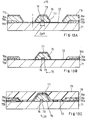
- Figures 1A to 1D illustrate the prior art process sequence for fabricating a semiconductor laser oscillator, a semiconductor light amplifier (or an LD amplifier) or a light modulator, and the band-gap controlling technology is incorporated in the prior art process sequence.
- the cross section is perpendicular to [011] orientation or the longitudinal direction of the semiconductor optical device.
- the prior art process sequence starts with an n-type semiconductor substrate 1 of indium phosphide, and (100)-oriented surface serves as the major surface for the optical device.
- a stripe mask 2 of silicon oxide which is 100 nm (1000 angstroms) in thickness and 10 microns in width.
- the stripe mask 2 is separated into two parts 2a and 2b by a spacing and the spacing is 2 microns wide.
- a buffer layer 3, an active layer 4 and a cladding layer are epitaxially grown on the exposed spacing area and form a mesa stripe.
- the active layer 4 is indium gallium arsenide phosphide layer of 1.55 micron wavelength composition, and is 2000 angstroms thick. The resultant structure of this stage is illustrated in figure 1A.
- the mask 2 on both sides of the mesa stripe is partially removed so that the exposed area is spread on both sides of the mesa stripe as shown in figure 1B.
- the selective MOVPE technique is employed again, and a cladding layer 6 and a cap layer 7 are grown over the mesa stripe on the exposed area as shown in figure 1C.
- the mesa stripe is buried in the cladding layer 6.
- the cladding layer 6 is formed of p-type indium phosphide, and is 1.5 micron thick.
- the cap layer 7 is formed of heavily doped p-type indium gallium arsenide, and is 200 nm (2000 angstroms) thick.
- silicon dioxide 100 nm (1000 angstroms) thick silicon dioxide is deposited on, and the silicon dioxide layer is partially removed so as to expose the top surface of the cap layer 7.
- the silicon dioxide layer and the mask 2 form passivation layer 8 covering the semiconductor optical device except for the cap layer 7.
- the substrate 1 of n-type indium phosphide and the cladding layer 6 of p-type indium phosphide form a homojunction 10 therebetween.
- the substrate 1 and the cladding layer 6 at the homo-junction 10 are of the order of 5 x 10 17 cm -3 in standard semiconductor optical devices.
- the electrode 9 If the electrode 9 is positively biased with respect to the substrate 1, current flows from the electrode 9 through the cap layer 7, the cladding layer 6, the cladding layer 5, the active layer 4, the buffer layer 3 into the substrate 1, and the active layer 4 generates laser light.
- the cladding layers 5 and 6 and the cap layer 7 are doped with n-type dopant impurity, and the buffer layer 3 is the p-type. As a result, the current flows in the opposite direction.
- the prior art process sequence is applicable to an electroabsorption modulator which uses the Franz-Keldysh effect, and the active layer 4 is replaced with a light absorption layer.
- the semiconductor optical device disclosed in the paper (1) has a waveguide in serial to the active layer 4, and the semiconductor optical device disclosed in the paper (3) further has a light absorbing layer in serial to the active layer 4. These waveguide and the light absorbing layer are formed through the band gap controlling technology, and the stripe-shaped masks disclosed in the papers (1) and 3 and the Japanese Patent Publication of Unexamined Application are oriented to [011] direction.
- the prior art semiconductor optical devices encounter a problem in output characteristics.
- the prior art semiconductor laser oscillator hardly achieves the light output exceeding 50 milli-watt, and the semiconductor light amplifier cannot achieve the light output exceeding 25 dB. This is because of the fact that the mesa-shaped structure is buried in the cladding layer 6, and the injected current partially flows across the homo-junction directly between the cladding layer 6 and the semiconductor substrate 1 without passing through the active layer 4.
- the prior art semiconductor light modulator is also affected by the homo-junction 10.
- the standard doping level of the substrate 1 and the cladding layer 6 near the homo-junction are of the order of 5 x 10 17 cm -3 .
- the total amount of parasitic capacitance including the capacitance at the electrode 9 is equal to or greater than 3 pF, and does not allow the modulation bandwidth more than 2.4 GHz. In order to achieve the band width 2.4 GHz, the total amount of parasitic capacitance should be not greater than 2 pF.
- a semiconductor opitcal device and a method for fabricating such a semiconductor optical device according to the precharacterizing part of claim 1 and claim 7, respectively, are disclosed in US-A-4,077,817.
- a semiconductor laser structure has side facets perpendicular to its substrate and a flat top.
- the central cavity is an elongated rectangular cavity.
- a substrate having (100) orientation has a mask patterned thereon with a window having an elongated central member and at least two cross members perpendicular to the axis of the elongated central member.
- the semiconductor material is grown thereon by liquid phase epitaxy.
- a further semiconductor device and the method of manufacturing the same are disclosed in EP-A-0 312 401.
- a semiconductor device comprises a semiconductor substrate having a surface orientation substantially in a (100)-orientation is provided.
- On the semiconductor substrate plural steps formed in a direction deviated substantially from a [100]-direction by 5 degrees or more are formed.
- the steps, which are mesa and concave portions, are buried by plural semiconductor crystal layers grown by the use of MOCVD or the like.
- the present invention proposes to isolate a cladding layer 21 overlain by a cap layer 22 from a semiconductor substrate 23 by an insulating mask layer 24 laterally surrounding a mesa structure 25 including a buffer layer 26 and an active layer 27 as shown in figure 2.
- the present inventor fabricated the semiconductor optical device shown in figure 2 through the prior art selective MOVPE technology, the selective MOVPE technology formed a cladding layer 21a and a cap layer 22a having a peak 28 as shown in figure 3.
- the present inventor contemplated the undesirable peak 28, and concluded that the insulating mask 24 oriented to [011] direction had resulted in the undesirable peak 28.
- a mesa 31 was selectively grown on an exposed center spacing 35a between the insulating mask 33 which is oriented to [011] direction, the mesa 31 firstly grew in a direction A vertical to the major surface of the semiconductor substrate 32, and had a flat top surface as shown in figure 4A.
- the mesa 31 thereafter grew in directions indicated by arrows B, and formed side surfaces 31b of (111) orientation merged at the peak 34 as shown in figure 4B to 4D.
- the peak 28 is not desirable, because an electrode requires a flat top surface of the cap layer.
- the present invention proposes to decline an exposed center spacing at least 5 degrees with respect to [011] direction.
- the present inventor confirmed the effect of the present invention.
- a semiconductor substrate 41 was exposed on the spacing between the insulating mask 42 obliquely extending at least 5 degrees with respect to [011] direction, a mesa 43 kept a trapezoid cross section through a selective MOVPE as shown in figures 5A to 5C.
- a semiconductor laser embodying the present invention is fabricated on a substrate 51 of n-type indium phosphide having a major surface 51a with (100) orientation.
- Arrow C is indicative of [011] direction of the substrate 51.
- the semiconductor laser embodying the present invention comprises an insulating mask 52 of silicon dioxide covering the major surface of the substrate 51, and is 100 nm (1000 angstroms) in thickness and 10 microns in width.
- the insulating mask 52 is split into two halves 52a and 52b spaced apart from each other by 2 microns, and a center spacing between the two halves 52a and 52b obliquely extends at a predetermined angle AG equal to or greater than 5 degrees with respect to [011] direction.
- the center spacing exposes a part of the major surface of the substrate 51.
- Figure 7 illustrates the layout of the insulating mask 52, and the two halves 52a and 52b are hatched for better understanding.
- the semiconductor laser embodying the present further comprises a buffer layer 53 of n-type indium phosphide grown over the part of the major surface and a multiple quantum well 54 with 1.48 micron wavelength composition grown over the buffer layer 53.
- the multiple quantum well 54 serves as an active layer, and includes six indium gallium arsenide layers each 40 angstroms thick and five indium gallium arsenic phosphide layers each 13 nm (130 angstroms) thick.
- the buffer layer 53 and the multiple quantum well 54 form in combination a mesa structure 55 having a trapezoid cross section, and the two halves 52a and 52b of the insulating mask 52 are held in contact with both sides of a lower portion of the mesa structure 55.
- the semiconductor laser embodying the present invention further comprises a cladding layer 56 of p-type indium phosphide 2.5 microns in height and a cap layer 57 of heavily doped p-type indium gallium arsenide 0.3 micron in thickness.
- the cladding layer 56 is grown from the mesa structure 55, and extends on an upper surface of the insulating mask 52. For this reason, the cladding layer 56 is not directly held in contact with the substrate 51.
- the cladding layer 56 has a flat top surface, and the cap layer 57 also form a flat top surface over the flat top surface of the cladding layer 56.
- the semiconductor laser embodying the present invention further comprises an insulating layer 58 of silicon dioxide topographically covering the cap layer 57 so as to create a flat top surface over the flat top surface of the cladding layer 56.
- the insulating layer 58 is 200 nm (2000 angstroms) thick, and a slit 58a is formed in the flat top surface of the insulating layer 58 for exposing the cap layer 57.
- the semiconductor laser embodying the present invention further comprises an electrode 59 covering the insulating layer 58 and held in contact with the cap layer 57 through the slit 58a, and the electrode 59 is implemented by a lamination including a gold film of 400 nm (4000 angstroms) thick and a titanium film of 50 nm (500 angstroms) thick.
- another electrode is held in contact with the back surface of the substrate 51.
- One of the device facet are coated with a reflecting film, and the reflecting film is about 95 per cent in reflectivity.
- the facets of opposite side are coated with anti-reflective film, and output light is emitted from the anti-reflective facet.
- the semiconductor laser thus arranged has a length of the order of 1 millimeter.
- the multiple quantum well may be replaced with a bulk active layer with 1.48 micron wavelength composition, and may be regulated to composition for 1.3 micron wavelength or composition for 1.55 micron wavelength.
- N-type indium phosphide, indium gallium arsenide and indium gallium arsenic phosphide are successively grown on the exposed center spacing through an metal organic vapor phase epitaxy.
- the n-type indium phosphide forms the buffer layer 53, and the six indium gallium arsenide layers and the five indium gallium arsenic phosphide layers alternately laminated on one another form in combination the multiple quantum well 54.
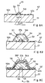
- the mesa structure 55 is formed on the exposed area as shown in figure 8A.
- the metal-organic vapor phase epitaxy further grows the cladding layer 56 of p-type indium phosphide and the cap layer 57 of heavily doped p-type indium gallium arsenic phosphide.
- the cladding layer 56 buries the mesa structure 55, and extends on the insulating mask 52.
- the cladding layer 56 reaches 2.5 micron high, and the cap layer is 0.3 micron thick. Even though cap layer 57 projects from the insulating mask layer by 2.8 microns, the cladding layer 56 and the cap layer 57 keep the top surfaces 56a and 57a flat as shown in figure 8B, because the mesa structure 55 obliquely extends at 5 degrees with respect to [011] direction.
- Silicon dioxide is deposited to 200 nm (2000 angstroms) thick over the entire surface of the structure, and the slit 58a is formed in the passivation film 58 for exposing the flat top surface 57a.
- Gold and titanium are deposited to 400 nm (4000 angstroms) thick and 50 nm (500 angstroms) thick over the entire surface of the passivation film 58, and the gold film and the titanium film form the electrode 59 through an alloying process.
- the resultant structure is illustrated in figure 8c.
- an electrode (not shown) is formed on the back surface of the substrate 51.
- the semiconductor laser are separated from one another through a cleavage step in such a manner as to be 1 millimeter in length.
- the injected current flows through the cladding layer 56 to the mesa structure 55 without leakage current, and achieves the large light output.
- the process sequence according to the present invention successively grows the buffer layer 53, the multiple quantum well 54, the cladding layer 56 and the cap layer 57 without partially removing stage for the insulating mask 52. Therefore, only one sequence of MOVPE process is required, while the prior art process require two sequence of MOVPE. In fact, the selective MOVPE is completed within half time period of the prior art process. Finally, the process sequence according to the present invention is good in reproducibility.
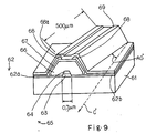
- a semiconductor optical amplifier or a semiconductor LD amplifier is fabricated on a substrate 61 of n-type indium phosphide.
- the n-type indium phosphide has a major surface 61a with (100) orientation, and arrow C' is indicative of [011] direction.
- the semiconductor optical amplifier is fabricated through the following process sequence.
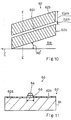
- An insulating mask 62 is provided on the major surface of the substrate 61, and the insulating mask 62 is split into two portions 62a and 62b spaced apart from one another by 0.7 micron as shown in figure 10.
- the portions 62a and 62b are 700 angstroms in thickness and 10 microns in width.
- the center spacing 62c obliquely extends at 10 degrees with respect to [011] direction, and exposes a part of the major surface 61a of the substrate 61.
- a buffer layer 63 of n-type indium phosphide and an active layer 64 of indium gallium arsenic phosphide are grown on the exposed center spacing 61a through a metal organic vapor phase epitaxy as shown in figure 11.
- the indium gallium arsenic phosphide is regulated to a predetermined composition for 1.3 micron wavelength, and is 300 nm (3000 angstroms) thick.
- the active layer 64 is 500 nm (5000 angstroms) wide at the intermediate point of the thickness, and the buffer layer 63 and the active layer 64 form in combination a mesa structure 65.
- the portions 62a and 62b are held in contact with the lower portion of the buffer layer 63.
- a cladding layer 66 of p-type indium phosphide and a cap layer 67 of heavily doped p-type indium gallium arsenide are continuously grown over the mesa structure 65 through the metal organic vapor phase epitaxy (see figure 9 again).
- the cladding layer 66 extends on the insulating mask 62, and is not directly contact with the major surface 61a.
- the cladding layer 66 is 1.5 micron high and the cap layer 67 is 0.3 micron thick, the top surfaces thereof are flat, because angle AG' is not less than 5 degrees.
- Silicon dioxide is topographically deposited to 200 nm (2000 angstroms) over the entire surface of the structure for forming an insulating layer 68, and a slit 68a is formed in the top surface of the passivation film 68 for exposing the flat top surface of the cap layer 67.
- Gold and titanium are deposited to 400 nm (4000 angstroms) thick and 50 nm (500 angstroms) thick over the entire surface of the structure, and the gold film and the titanium film are formed into an electrode 69 through an alloying technique.
- the back surface of the substrate 61 is grinded, and, thereafter, an electrode is provided on the grinded back surface.
- the semiconductor light amplifiers are separated through a cleavage, and the device length is regulated to 500 microns.
- the active layer 64 may be formed of indium gallium arsenic phosphide with 1.55 micron wavelength composition for incident light with 1.55 micron wavelength.
- the semiconductor light amplifier achieves a large gain, because the current flows into the active layer without leakage current into the substrate 61, and the process sequence is simpler than the prior art process.
- the process sequence according to the present invention is good in reproducibility.
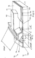
- a electroabsorption optical modulator embodying the present invention is fabricated on a substrate 71 of n-type indium phosphide.
- the indium phosphide crystal has (100) surface serving as a major surface of the substrate 71.
- an insulating mask 72 is provided on the major surface, and is split into two portions 72a and 72b spaced apart from one another by a 2 micron wide center spacing.
- the two portions 72a and 72b are 300 nm (3000 angstroms) in thick and 15 microns wide.
- the center spacing obliquely extends at 10 degrees with respect to [011] direction indicated by arrow C''.
- a buffer layer 73 of n-type indium phosphide and an optical absorbing layer 74 are successively grown on the exposed area of the major surface of the substrate 71.
- the optical absorbing layer 74 is 250 nm (2500 angstroms) thick, and the indium gallium arsenic phosphide is regulated to the 1.45 micron wavelength composition.
- the buffer layer 73 and the optical absorbing layer 74 form a mesa structure 75.
- the metal organic vapor phase epitaxy further grows a cladding layer 76 of p-type indium phosphide and a cap layer 77 of heavily doped p-type indium gallium arsenide over the mesa structure 75, and the insulating mask 72 prevents the cladding layer 76 and the substrate 71 from direct contact.
- the cladding layer 76 is 1.5 micron high, and the cap layer 77 is 0.3 micron thick.
- the cladding layer 76 and the cap layer 77 keep the top surfaces thereof flat, because the mesa structure 75 is grown on the exposed center spacing declining at more than 5 degrees with respect to [011] direction.
- an n-type indium phosphide layer 73a, an indium gallium arsenic phosphide layer 74a, a p-type indium phosphide layer and a heavily doped p-type indium gallium arsenide layer are simultaneously grown on the major surface outside of the insulating mask 72 as shown in figure 13A.
- These layers 76a to 77a are etched away by at least 1 micron thick as shown in figure 13B. Silicon dioxide is deposited over the entire surface of the structure to 200 nm (2000 angstroms) thick so as to form a passivation layer 78, and the passivation layer 78 is coated with polyimide 79 as shown in figure 13C.
- the polyimide layer 79 and the passivation layer 78 are partially removed to expose the flat top surface of the cap layer 77, and gold and titanium are deposited to 4000 angstroms and 50 nm (500 angstroms) over the entire surface of the structure.
- the gold film, the titanium film and the polyimide layer 79 are patterned as shown in figure 12.
- the gold film and the titanium film are formed into an electrode 80 through an alloying step.
- the substrate is made thinner by back surface etching.
- An electrode (not shown) is formed on the back surface, and the semiconductor optical modulator with a device length of 300 microns is separated through a cleavage.
- An anti-reflective film (not shown) covers the device facets.
- the electroabsorption optical modulator embodying the present invention achieved the extinction ratio at 20 dB, the optical loss at 3 dB and the modulation band width of 5 GHz.
- the coupling loss was 2.5 dB.
- the insulating mask 72 was 300 nm (3000 angstroms) thick. However, if the insulating mask 72 of silicon dioxide is not less than 200 nm (2000 angstroms), the modulation bandwidth of 2.4 GHz is achievable.
- the optical absorbing layer 74 may be replaced with a multiple quantum well structure implemented by an alternately laminated six indium gallium arsenide layers each 3 nm (30 angstroms) thick and five indium gallium arsenic phosphide layers with 1.3 micron wavelength composition each 13 nm (130 angstroms) thick.
- the structure is of oscillating wavelength of 1.45 microns composition.
- the insulating mask layer 72 prevents the substrate 71 from leakage current from the cladding layer 76, and the thick insulating mask 72 decreases the parasitic capacitance not greater than 1 pF.
- the electroabsorption optical modulator according to the present invention achieves the good performances.
- the process sequence according to the present invention grows the buffer layer 73 to the cap layer 77 through a single metal organic vapor phase epitaxy, and, for this reason, is simpler than the prior art process sequence without sacrifice of reproducibility.
- the selectively growing technology is not limited to the metal organic vapor phase epitaxy, and the compound semiconductor materials used for the semiconductor optical device may be in a different system.
- the semiconductor optical devices according to the present invention may be fabricated on p-type semiconductor substrates by changing the dopant impurities of the compound semiconductor layers to the opposite type to those of the semiconductor optical devices described hereinbefore.
- the insulating mask layers, the insulating layers and the passivation layer may be formed of PSG or SiON.
Landscapes
- Physics & Mathematics (AREA)
- Optics & Photonics (AREA)
- Nonlinear Science (AREA)
- General Physics & Mathematics (AREA)
- Chemical & Material Sciences (AREA)
- Engineering & Computer Science (AREA)
- Nanotechnology (AREA)
- Electromagnetism (AREA)
- Condensed Matter Physics & Semiconductors (AREA)
- Geometry (AREA)
- Life Sciences & Earth Sciences (AREA)
- Biophysics (AREA)
- Crystallography & Structural Chemistry (AREA)
- Semiconductor Lasers (AREA)
Claims (7)
- Dispositif optique à semi-conducteurs fabriqué sur un substrat semi-conducteur (51 ; 61 ; 71), comportant :a) un masque isolant (52 ; 62 ; 72) recouvrant une surface dudit substrat semi-conducteur,b) une structure mesa semi-conductrice (55 ; 65 ; 75) formée par croissance épitaxiale sur une partie de ladite surface dudit substrat semi-conducteur qui possède l'orientation (100), ladite couche formant masque isolant comportant un espace (62c) en forme de bande laissant exposée ladite partie de ladite surface de manière à permettre à une partie inférieure de ladite structure mesa d'être maintenue en contact avec ladite partie de ladite surface et avec ledit masque isolant,c) une couche de placage (56 ; 66 ; 76) formée par croissance épitaxiale sur ladite structure mesa semi-conductrice, et s'étendant sur ladite couche formant masque isolant sans contact direct avec ledit substrat semi-conducteur, etd) une couche de recouvrement (57 ; 67 ; 77) formée par croissance épitaxiale qui recouvre ladite couche de placage,caractérisé en ce queladite structure mesa semi-conductrice, ladite couche de placage et ladite couche de recouvrement sont formées par croissance en utilisant une épitaxie en phase vapeur,ledit espace en forme de bande s'étendant à l'oblique en formant un angle de 5 degrés ou plus par rapport à la direction [011] de la structure cristalline dudit substrat semi-conducteur.
- Dispositif optique à semi-conducteurs selon la revendication 1, dans lequel ladite structure mesa comporte un puits quantique multiple pour produire une lumière laser.
- Dispositif optique à semi-conducteurs selon la revendication 1, dans lequel ladite structure mesa comporte une couche active pour amplifier une lumière incidente.
- Dispositif optique à semi-conducteurs selon la revendication 1, dans lequel ladite structure mesa comporte une couche absorbant la lumière pour moduler une lumière incidente.
- Dispositif optique à semi-conducteurs selon l'une quelconque des revendications 2, 3 et 4, dans lequel ladite structure mesa comporte de plus une couche tampon située entre ledit substrat et ladite couche absorbant la lumière.
- Dispositif optique à semi-conducteurs selon la revendication 1, dans lequel la nature et l'épaisseur de ladite couche formant masque isolant sont telles que la capacité électrique parasite n'est pas supérieure à 2 pF.
- Procédé de fabrication d'un dispositif optique à semi-conducteurs, comportant les étapes consistant à :a) préparer un substrat semi-conducteur (51; 61 ; 71) ayant une surface principale (61a) d'orientation (100) et une structure cristalline de direction [011] s'étendant sur ladite surface principale ;b) disposer une couche formant masque isolant (52 ; 62 ; 72) sur ladite surface principale, ladite couche formant masque isolant comportant un espace en forme de bande (62c) laissant exposée une partie de ladite surface principale ;c) former par croissance une structure mesa (55 ; 65 ; 75) sur ladite partie de ladite surface principale de sorte que ladite couche formant masque isolant soit maintenue en contact avec une partie inférieure de ladite structure mesa ;d) former successivement par croissance une couche de placage (56 ; 66 ; 76) et une couche de recouvrement (57 ; 67 ; 77) sur ladite structure mesa et s'étendant sur une surface supérieure de ladite couche formant masque isolant ;e) former une électrode (59 ; 69) connectée électriquement à ladite couche de placage pour fournir un courant à travers ladite couche de placage à ladite structure mesa,caractérisé en ce que ladite structure mesa semi-conductrice et ladite couche de placage sont formées par croissance en utilisant une épitaxie en phase vapeur dans des conditions dans lesquelles ledit espace en forme de bande s'étend à l'oblique en formant un angle de 5 degrés ou plus par rapport à la direction [011] de la structure cristalline dudit substrat semi-conducteur de manière à obtenir une surface plate (56a) pour ladite couche de placage et une surface plate (57a) pour ladite couche de recouvrement avec laquelle ladite électrode est maintenue en contact.
Applications Claiming Priority (2)
| Application Number | Priority Date | Filing Date | Title |
|---|---|---|---|
| JP5187803A JP2746065B2 (ja) | 1993-07-29 | 1993-07-29 | 光半導体素子の製造方法 |
| JP187803/93 | 1993-07-29 |
Publications (2)
| Publication Number | Publication Date |
|---|---|
| EP0637111A1 EP0637111A1 (fr) | 1995-02-01 |
| EP0637111B1 true EP0637111B1 (fr) | 1997-12-29 |
Family
ID=16212516
Family Applications (1)
| Application Number | Title | Priority Date | Filing Date |
|---|---|---|---|
| EP94111723A Expired - Lifetime EP0637111B1 (fr) | 1993-07-29 | 1994-07-27 | Dispositif optique à semi-conducteur avec structure mesa qui est entournée latéralement par un masque isolant |
Country Status (5)
| Country | Link |
|---|---|
| US (1) | US5659565A (fr) |
| EP (1) | EP0637111B1 (fr) |
| JP (1) | JP2746065B2 (fr) |
| CA (1) | CA2129074A1 (fr) |
| DE (1) | DE69407507T2 (fr) |
Cited By (1)
| Publication number | Priority date | Publication date | Assignee | Title |
|---|---|---|---|---|
| CN109983639A (zh) * | 2016-11-29 | 2019-07-05 | 三菱电机株式会社 | 光器件 |
Families Citing this family (14)
| Publication number | Priority date | Publication date | Assignee | Title |
|---|---|---|---|---|
| GB9523731D0 (en) | 1995-11-20 | 1996-01-24 | British Telecomm | Optical transmitter |
| AU1887297A (en) * | 1996-03-27 | 1997-10-17 | British Telecommunications Public Limited Company | Optical modulator |
| JP3682336B2 (ja) * | 1996-04-10 | 2005-08-10 | 三菱電機株式会社 | 半導体レーザ装置の製造方法 |
| SE9902916L (sv) * | 1999-08-16 | 2001-02-17 | Ericsson Telefon Ab L M | Modulator och integrerad krets |
| JP2001313439A (ja) * | 2000-04-28 | 2001-11-09 | Oki Electric Ind Co Ltd | 半導体レーザの製造方法 |
| US6563852B1 (en) * | 2000-05-08 | 2003-05-13 | Lucent Technologies Inc. | Self-mode-locking quantum cascade laser |
| SE521023C2 (sv) * | 2000-07-07 | 2003-09-23 | Ericsson Telefon Ab L M | Optisk anordning samt framställning därav |
| JP3912117B2 (ja) * | 2002-01-17 | 2007-05-09 | ソニー株式会社 | 結晶成長方法、半導体発光素子及びその製造方法 |
| JP3878868B2 (ja) | 2002-03-01 | 2007-02-07 | シャープ株式会社 | GaN系レーザ素子 |
| US7184640B2 (en) * | 2004-02-25 | 2007-02-27 | Avago Technologies Fiber Ip (Singapore) Pte. Ltd. | Buried heterostructure device fabricated by single step MOCVD |
| US7440666B2 (en) * | 2004-02-25 | 2008-10-21 | Avago Technologies Fiber Ip (Singapore) Pte. Ltd. | Buried heterostucture device having integrated waveguide grating fabricated by single step MOCVD |
| US7539228B2 (en) * | 2007-06-26 | 2009-05-26 | Avago Technologies Fiber Ip (Singapore) Pte. Ltd. | Integrated photonic semiconductor devices having ridge structures that are grown rather than etched, and methods for making same |
| JP5374894B2 (ja) * | 2008-03-18 | 2013-12-25 | 富士通株式会社 | 半導体光増幅器及びその製造方法並びに半導体光集積素子 |
| FR3007589B1 (fr) * | 2013-06-24 | 2015-07-24 | St Microelectronics Crolles 2 | Circuit integre photonique et procede de fabrication |
Family Cites Families (15)
| Publication number | Priority date | Publication date | Assignee | Title |
|---|---|---|---|---|
| US4077817A (en) | 1975-12-31 | 1978-03-07 | Texas Instruments Incorporated | Making a semiconductor laser structure by liquid phase epitaxy |
| JPS6194389A (ja) * | 1984-10-16 | 1986-05-13 | Matsushita Electric Ind Co Ltd | 半導体レ−ザ−素子の製造方法 |
| FR2587852B1 (fr) * | 1985-09-24 | 1989-04-07 | Chaminant Guy | Procede de realisation d'un laser a semiconducteur a ruban enterre avec ou sans reseau de diffraction et laser obtenu par ce procede |
| JPS6473690A (en) * | 1987-09-14 | 1989-03-17 | Mitsubishi Electric Corp | Manufacture of semiconductor laser |
| DE3886337D1 (de) * | 1987-10-15 | 1994-01-27 | Toshiba Kawasaki Kk | Halbleiteranordnungen und Herstellungsverfahren. |
| JPH0834336B2 (ja) * | 1990-01-31 | 1996-03-29 | シャープ株式会社 | 半導体レーザ素子及びその製造方法 |
| US5070510A (en) * | 1989-12-12 | 1991-12-03 | Sharp Kabushiki Kaisha | Semiconductor laser device |
| JPH03227586A (ja) * | 1990-02-01 | 1991-10-08 | Nec Corp | 半導体レーザ |
| JP3078004B2 (ja) * | 1990-08-31 | 2000-08-21 | 株式会社東芝 | 半導体レーザの製造方法 |
| JPH04243216A (ja) * | 1991-01-17 | 1992-08-31 | Nec Corp | 光導波路の製造方法ならびに光集積素子及びその製造方法 |
| JP2876839B2 (ja) * | 1991-07-31 | 1999-03-31 | 日本電気株式会社 | 光半導体素子の製造方法 |
| JPH0548215A (ja) * | 1991-08-21 | 1993-02-26 | Fuji Xerox Co Ltd | 半導体レーザダイオードおよびその製造方法 |
| JPH05110186A (ja) * | 1991-10-14 | 1993-04-30 | Nippon Telegr & Teleph Corp <Ntt> | モノリシツク光素子およびその製造方法 |
| JPH05145192A (ja) * | 1991-11-25 | 1993-06-11 | Toshiba Corp | 半導体光増幅器並びにその製造方法 |
| JPH06204454A (ja) * | 1992-12-28 | 1994-07-22 | Mitsubishi Electric Corp | 光変調器付半導体レーザ及びその製造方法 |
-
1993
- 1993-07-29 JP JP5187803A patent/JP2746065B2/ja not_active Expired - Fee Related
-
1994
- 1994-07-27 US US08/280,680 patent/US5659565A/en not_active Expired - Fee Related
- 1994-07-27 DE DE69407507T patent/DE69407507T2/de not_active Expired - Fee Related
- 1994-07-27 EP EP94111723A patent/EP0637111B1/fr not_active Expired - Lifetime
- 1994-07-28 CA CA002129074A patent/CA2129074A1/fr not_active Abandoned
Cited By (1)
| Publication number | Priority date | Publication date | Assignee | Title |
|---|---|---|---|---|
| CN109983639A (zh) * | 2016-11-29 | 2019-07-05 | 三菱电机株式会社 | 光器件 |
Also Published As
| Publication number | Publication date |
|---|---|
| CA2129074A1 (fr) | 1995-01-30 |
| JP2746065B2 (ja) | 1998-04-28 |
| JPH0745906A (ja) | 1995-02-14 |
| EP0637111A1 (fr) | 1995-02-01 |
| US5659565A (en) | 1997-08-19 |
| DE69407507T2 (de) | 1998-07-23 |
| DE69407507D1 (de) | 1998-02-05 |
Similar Documents
| Publication | Publication Date | Title |
|---|---|---|
| JP3285426B2 (ja) | 半導体光集積素子及びその製造方法 | |
| US5825047A (en) | Optical semiconductor device | |
| EP0637111B1 (fr) | Dispositif optique à semi-conducteur avec structure mesa qui est entournée latéralement par un masque isolant | |
| US5987046A (en) | Optical semiconductor device and a method of manufacturing the same | |
| US6121068A (en) | Long wavelength light emitting vertical cavity surface emitting laser and method of fabrication | |
| EP0472221A2 (fr) | Méthode pour la fabrication d'un dispositif optique à semi-conducteur | |
| EP0663710B1 (fr) | Dispositif optique à semi-conducteur et méthode de fabrication | |
| US7476558B2 (en) | Method for manufacturing selective area grown stacked-layer electro-absorption modulated laser structure | |
| GB2282483A (en) | Semiconductor laser/modulator device | |
| JP2008113041A (ja) | 導波管 | |
| GB2301481A (en) | Semiconductor laser | |
| JPH11220212A (ja) | 光素子、光素子の駆動方法及び半導体レーザ素子 | |
| EP0874425B1 (fr) | Laser à semiconducteur à l'émission par la surface avec cavité du type anneau | |
| JPH04397B2 (fr) | ||
| US6931041B2 (en) | Integrated semiconductor laser device and method of manufacture thereof | |
| US6482665B1 (en) | Polarization switching surface-emitting laser and a method of manufacturing the same | |
| JPH04105383A (ja) | 半導体光集積素子の製造方法 | |
| KR0174303B1 (ko) | 반도체장치 및 그 제조방법 | |
| US6489177B1 (en) | Modulator-integrated semiconductor laser and method of fabricating the same | |
| US5811838A (en) | Electro-absorption type semiconductor optical modulator | |
| CA2033246C (fr) | Dispositif optique a semiconducteur | |
| US20060108574A1 (en) | Optoelectronic transmitter integrated circuit and method of fabricating the same using selective growth process | |
| EP1372229B1 (fr) | Element integré composé d'un laser semiconducteur et d'un guide d'ondes | |
| US5397740A (en) | Method of making an optical semiconductor device | |
| JP2000101186A (ja) | 半導体光素子およびその製造方法 |
Legal Events
| Date | Code | Title | Description |
|---|---|---|---|
| PUAI | Public reference made under article 153(3) epc to a published international application that has entered the european phase |
Free format text: ORIGINAL CODE: 0009012 |
|
| AK | Designated contracting states |
Kind code of ref document: A1 Designated state(s): DE FR GB |
|
| 17P | Request for examination filed |
Effective date: 19941209 |
|
| 17Q | First examination report despatched |
Effective date: 19950817 |
|
| GRAG | Despatch of communication of intention to grant |
Free format text: ORIGINAL CODE: EPIDOS AGRA |
|
| GRAG | Despatch of communication of intention to grant |
Free format text: ORIGINAL CODE: EPIDOS AGRA |
|
| GRAH | Despatch of communication of intention to grant a patent |
Free format text: ORIGINAL CODE: EPIDOS IGRA |
|
| GRAH | Despatch of communication of intention to grant a patent |
Free format text: ORIGINAL CODE: EPIDOS IGRA |
|
| GRAA | (expected) grant |
Free format text: ORIGINAL CODE: 0009210 |
|
| AK | Designated contracting states |
Kind code of ref document: B1 Designated state(s): DE FR GB |
|
| REF | Corresponds to: |
Ref document number: 69407507 Country of ref document: DE Date of ref document: 19980205 |
|
| ET | Fr: translation filed | ||
| PLBE | No opposition filed within time limit |
Free format text: ORIGINAL CODE: 0009261 |
|
| STAA | Information on the status of an ep patent application or granted ep patent |
Free format text: STATUS: NO OPPOSITION FILED WITHIN TIME LIMIT |
|
| 26N | No opposition filed | ||
| REG | Reference to a national code |
Ref country code: GB Ref legal event code: IF02 |
|
| PGFP | Annual fee paid to national office [announced via postgrant information from national office to epo] |
Ref country code: FR Payment date: 20020709 Year of fee payment: 9 |
|
| PGFP | Annual fee paid to national office [announced via postgrant information from national office to epo] |
Ref country code: GB Payment date: 20020724 Year of fee payment: 9 |
|
| PGFP | Annual fee paid to national office [announced via postgrant information from national office to epo] |
Ref country code: DE Payment date: 20020731 Year of fee payment: 9 |
|
| PG25 | Lapsed in a contracting state [announced via postgrant information from national office to epo] |
Ref country code: GB Free format text: LAPSE BECAUSE OF NON-PAYMENT OF DUE FEES Effective date: 20030727 |
|
| PG25 | Lapsed in a contracting state [announced via postgrant information from national office to epo] |
Ref country code: DE Free format text: LAPSE BECAUSE OF NON-PAYMENT OF DUE FEES Effective date: 20040203 |
|
| GBPC | Gb: european patent ceased through non-payment of renewal fee |
Effective date: 20030727 |
|
| PG25 | Lapsed in a contracting state [announced via postgrant information from national office to epo] |
Ref country code: FR Free format text: LAPSE BECAUSE OF NON-PAYMENT OF DUE FEES Effective date: 20040331 |
|
| REG | Reference to a national code |
Ref country code: FR Ref legal event code: ST |