EP0640925B1 - Système de traitement de données avec interface sériel - Google Patents
Système de traitement de données avec interface sériel Download PDFInfo
- Publication number
- EP0640925B1 EP0640925B1 EP94113156A EP94113156A EP0640925B1 EP 0640925 B1 EP0640925 B1 EP 0640925B1 EP 94113156 A EP94113156 A EP 94113156A EP 94113156 A EP94113156 A EP 94113156A EP 0640925 B1 EP0640925 B1 EP 0640925B1
- Authority
- EP
- European Patent Office
- Prior art keywords
- transmission
- data
- serial interface
- interrupt
- response
- Prior art date
- Legal status (The legal status is an assumption and is not a legal conclusion. Google has not performed a legal analysis and makes no representation as to the accuracy of the status listed.)
- Expired - Lifetime
Links
Images


Classifications
-
- G—PHYSICS
- G06—COMPUTING OR CALCULATING; COUNTING
- G06F—ELECTRIC DIGITAL DATA PROCESSING
- G06F13/00—Interconnection of, or transfer of information or other signals between, memories, input/output devices or central processing units
- G06F13/38—Information transfer, e.g. on bus
-
- G—PHYSICS
- G06—COMPUTING OR CALCULATING; COUNTING
- G06F—ELECTRIC DIGITAL DATA PROCESSING
- G06F13/00—Interconnection of, or transfer of information or other signals between, memories, input/output devices or central processing units
- G06F13/14—Handling requests for interconnection or transfer
- G06F13/20—Handling requests for interconnection or transfer for access to input/output bus
- G06F13/24—Handling requests for interconnection or transfer for access to input/output bus using interrupt
-
- G—PHYSICS
- G06—COMPUTING OR CALCULATING; COUNTING
- G06F—ELECTRIC DIGITAL DATA PROCESSING
- G06F13/00—Interconnection of, or transfer of information or other signals between, memories, input/output devices or central processing units
- G06F13/38—Information transfer, e.g. on bus
- G06F13/382—Information transfer, e.g. on bus using universal interface adapter
- G06F13/385—Information transfer, e.g. on bus using universal interface adapter for adaptation of a particular data processing system to different peripheral devices
Definitions
- the present invention relates to a data processing system such as a microcomputer, having a serial interface.
- the vector interrupt is that a program counter (PC) and a program status word (PSW) is automatically saved to a stack memory and an operation is branched into an interrupt processing routine so as to execute a predetermined program written by macro-instructions.
- the macroservice is that, in response to an interrupt request, a data transfer is performed, by a hardware, between a special function register and a memory space.
- the CPU temporarily stops execution of the program, and automatically carries out a data transfer of one or two bytes between the special function register and the memory.
- the interrupt request flag is reset, and the CPU resumes the execution of the program.
- the vector interrupt request is generated.
- this macroservice processing does not activate an interrupt processing program, but automatically performs a predetermined processing stored in a microprogram ROM (read only memory). Accordingly, a series of operations including the branching to the interrupt service routine, the saving and returning of the registers, the returning from the interrupt service routine, is not performed. Accordingly, it is possible to elevate the service time of the CPU and to reduce the number of steps in the program.
- FIG. 1 there is shown a block diagram of one typical example of the conventional data processor having a serial interface.
- the shown data processor includes a CPU 1, an interrupt controller (INTC) 2 and a serial interface 3, which are interconnected through an internal bus 4.
- IRC interrupt controller
- the interrupt controller 2 If the interrupt controller 2 receives the request signal REQ from the serial interface 3, the interrupt controller 2 discriminates the priority order of the interrupt and the status of the interrupt mask. If it is permissible to acknowledge the request signal REQ, the interrupt controller 2 asynchronously outputs an interrupt request signal INTREQ to the CPU 1.
- the CPU includes a macroservice counter (MSC) 1A, which can be formed by utilizing for example an internal RAM (random access memory).
- FIG. 2 there is shown a detailed circuit diagram of the serial interface 3.
- a transmission shift register 31 of for example eight bits is set with the data on the internal bus 4 which is also of eight bits in this case.
- the 8-bit data stored in the shift register 31 is shifted in response to a serial clock CLK so as to be serially outputted through an output buffer 32 form the output terminal OUT.
- a serial transmission is carried out.
- All stages or bits of the transmission shift register 31 are coupled to a transmission end detection circuit 33, which is configured to detect whether or not the transmission shift register 31 becomes empty, for the purpose of detecting completion of the transmission of the 8-bit data.
- This transmission end detection circuit 33 generates the above mentioned request signal REQ.
- this transmission end detection circuit 33 can be constituted of an eight-input exclusive-OR circuit.
- the number of serial transmissions is firstly set into the macroservice counter 1A which is managed in the course of the macroservice processing, in order to ensure that a predetermined number of macroservices are performed.
- the value MS/ INT of the status flag register 2A in the interrupt controller 2 is previously set to "1".
- the data set into the transmission shift register 31 is serially outputted from the output terminal OUT in synchronism with the serial clock CLK.
- the request signal REQ is generated by the serial interface 3.
- the interrupt request signal INTREQ is generated by the interrupt controller 2, and sent to the CPU 1. Since the value MS / INT of the status flag register 2A in the interrupt controller 2 is 0 (zero) which designates the vector interrupt, the CPU 1 activates a microprogram for the vector interrupt, so that a vector interrupt processing program is activated.
- Japanes patent JP-60183639 describes a data processing system with a serial interface in which data transfer can be performed either by vector interrupt processing or by a macroservice function.
- Another object of the present invention is to provide a data processing which has a serial interface and which can transfer new data to a serial transmission shift register in a serial interface, at an appropriate timing with no wasteful waiting time, in a vector interrupt processing just after completion of a macroservice function processing.
- a data processor comprising a bus, a central processing unit coupled to the bus, an interrupt controller coupled to the bus and asynchronously generating a processing request to the central processing unit, and a serial interface coupled to the bus and for serially outputting data to an external.
- the serial interface is configured to receive data to be transmitted, from the central processing unit through the bus and to serially transmit the received data to the external.
- the serial interface includes a transmission end flag which is brought into a first condition in response to the starting of the transmission of data of one transmission unit and also brought into a second condition different from the first condition, in response to completion of the transmission of the data of one transmission unit.
- the interrupt controller is configured to receive a request signal from the serial interface and to output an interrupt request signal to the central processing unit.
- the interrupt controller includes a status flag indicative of whether an operation is in a macroservice processing or in a vector interrupt processing.
- the central processing unit is configured to respond to the interrupt request signal to execute one of the macroservice processing and the vector interrupt processing designated by the status flag.
- the central processing unit is also configured to change the status flag to a value indicative of the vector interrupt processing after completion of the macroservice processing.
- the central processing unit is further configured to discriminate the condition of the transmission end flag in the course of the vector interrupt processing so as to transfer new data to the serial interface in accordance with the condition of the transmission end flag.
- the data processor in accordance with the present invention is characterized by provision, in the serial interface, of the transmission end flag which is brought into the first condition in response to the starting of the transmission of data of one transmission unit and also brought into the second condition in response to completion of the transmission of the data of one transmission unit.
- the CPU watches and discriminates the condition of the transmission end flag in a programmed operation of the CPU, thereby capable of detecting a timing where the data to be transmitted is transferred to the transmission shift register.
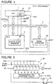
- FIG 4 there is shown a block diagram of one embodiment of the data processor having a serial interface and in accordance with the present invention.
- elements similar or corresponding to those shown in Figure 1 will be given the same Reference Numerals and Signs, and explanation thereof will be omitted.
- the embodiment shown in Figure 4 is different from the conventional data processor shown in Figure 1, in that a transmission end flag signal FLG indicative of completion of the data transmission from the transmission shift register 31 is outputted from a serial interface 3A to the CPU 1.
- the serial interface 3A is constructed as shown in Figure 5.
- elements similar or corresponding to those shown in Figure 2 will be given the same Reference Numerals and Signs, and explanation thereof will be omitted.
- the serial interface 3A shown in Figure 5 is different from the conventional serial interface 3 shown in Figure 2, in that a RS flipflop (reset/set flipflop) 34 is added, which includes a set input "S" connected to receive the transmission start signal ST and a reset input "R” connected to receive the request signal REQ outputted from the transmission end detection circuit 33.
- An output "Q" of the RS flipflop 34 generates the above mentioned transmission end flag signal FLG.
- the request signal REQ is generated by the serial interface 3A. If no interrupt signal is generated by the other interrupt sources, the interrupt request signal INTREQ is generated by the interrupt controller 2, and sent to the CPU 1. At this time, since the value MS/ INT of the status flag register 2A in the interrupt controller 2 is 0 (zero) which designates the vector interrupt, the CPU 1 activates a microprogram for the vector interrupt, so that a vector interrupt processing program is activated.
- the CPU 1 watches the transmission end flag signal FLG of the serial interface 3A at predetermined constant intervals in the course of execution of a vector interrupt processing program. If the transmission end flag signal FLG is "1", the CPU 1 does not transfer a new byte of data to be transmitted, to the serial interface 3A. If the transmission shift register 31 becomes empty, namely, if the transmission end flag signal FLG becomes "0" (zero) which means that the CPU 1 can transfer a new byte of data to be transmitted to the serial interface 3A, the CPU 1 transfers a new byte of data to be transmitted, to the serial interface 3A, in accordance with the vector interrupt processing program.
- a polling of the transmission end flag FLG constituted of the RS flipflop 34 in the serial interface 3A is carried out by reading the transmission end flag FLG in the vector interrupt processing for the purpose of discriminating the condition of the transmission end flag FLG, and by executing a conditional branch instruction on the basis of the result of the discrimination of the transmission end flag FLG.
- the transmission end flag FLG can be allocated to these free spaces, so that the polling of the transmission end flag FLG can be executed with only one conditional branch instruction.
- the CPU has a function of polling the transmission end flag FLG on the basis of the vector interrupt processing program.
- the embodiment is such chat the RS flipflop for the transmission end flag FLG is set by the transmission start signal ST and reset by the request signal REQ.
- the RS flipflop can be reset by the transmission start signal ST and set by the request signal REQ. Either situation can be treated by a program.
- the timing of transferring data to the transmission shift register can be detected by watching the transmission end flag. Therefore, it is possible to solve the disadvantage of the conventional data processor in which since it is not possible in a programmed operation to discriminate whether or not it is permissible to transfer data to the transmission shift register, the data is transferred to the transmission shift register with a sufficient delay time, or alternatively, it is inhibited to transfer data to the transmission shift register in the course of the vector interrupt processing. In other words, it is possible to eliminate the mismatching between the serial transmission status of the transmission shift register and the software processing of the CPU.
Landscapes
- Engineering & Computer Science (AREA)
- Theoretical Computer Science (AREA)
- Physics & Mathematics (AREA)
- General Engineering & Computer Science (AREA)
- General Physics & Mathematics (AREA)
- Information Transfer Systems (AREA)
- Computer And Data Communications (AREA)
- Communication Control (AREA)
Claims (3)
- Processeur de données comprenant un bus (4), une unité centrale de traitement (1) couplée audit bus, une unité de commande d'interruption (2) couplée audit bus et générant de manière asynchrone une demande de traitement vers ladite unité centrale de traitement, et une interface sérielle (3A) couplée audit bus et pour sortir de manière sérielle des données vers l'extérieur,ladite interface sérielle étant configurée pour recevoir des données à transmettre depuis ladite unité centrale de traitement par l'intermédiaire dudit bus et pour transmettre sériellement les données reçues vers l'extérieur, ladite interface sérielle comportant un drapeau de fin de transmission qui est placé dans une première condition en réponse au début de la transmission de données d'une longueur unitaire de transmission et qui est aussi placé dans une deuxième condition, différente de la première condition, en réponse à l'achèvement de la transmission desdites données d'une longueur unitaire de transmission,ladite unité de commande d'interruption étant configurée pour recevoir un signal de demande (REQ) provenant de ladite interface sérielle et pour sortir un signal de demande d'interruption (INTREQ) vers ladite unité centrale de traitement, ladite unité de commande d'interruption comportant un drapeau d'état indiquant si une opération est dans un traitement de macroservice ou dans un traitement d'interruption vectorisée,ladite unité centrale de traitement étant configurée pour répondre audit signal de demande d'interruption pour exécuter l'un dudit traitement de macroservice et dudit traitement d'interruption vectorisée désigné par ledit drapeau d'état, ladite unité centrale, de traitement étant aussi configurée pour changer ledit drapeau d'état à une valeur indiquant ledit traitement d'interruption vectorisée après l'achèvement dudit traitement de macroservice, ladite unité centrale de traitement étant aussi configurée pour discriminer la condition dudit drapeau de fin de transmission au cours dudit traitement d'interruption vectorisée afin de transférer de nouvelles données vers ladite interface sérielle lorsque la condition dudit drapeau de fin de transmission indique l'achèvement de la transmission précédente.
- Processeur de données selon la revendication 1, dans lequel ladite interface sérielle comporte un registre à décalage de transmission (31) chargé de données par l'intermédiaire dudit bus depuis ladite unité centrale de traitement en réponse à un signal de début de transmission provenant de ladite unité centrale de traitement, ledit registre à décalage de transmission fonctionnant de manière à sortir sériellement lesdites données en réponse à une horloge sérielle, et un circuit de détection de fin de transmission (33) connecté à tous les bits dudit registre à décalage de transmission pour détecter le vide dudit registre à décalage de transmission afin de générer ledit signal de demande, ledit drapeau de fin de transmission étant sorti dans ladite première condition en réponse audit signal de début de transmission et étant sorti dans ladite deuxième condition en réponse audit signal de demande.
- Processeur de données selon la revendication 2, dans lequel ledit drapeau de fin de transmission est formé par une bascule RS (34) instaurée en réponse audit signal de début de transmission et restaurée en réponse audit signal de demande.
Applications Claiming Priority (2)
| Application Number | Priority Date | Filing Date | Title |
|---|---|---|---|
| JP229451/93 | 1993-08-23 | ||
| JP5229451A JPH0764886A (ja) | 1993-08-23 | 1993-08-23 | シリアルインターフェイス装置を有する処理装置 |
Publications (2)
| Publication Number | Publication Date |
|---|---|
| EP0640925A1 EP0640925A1 (fr) | 1995-03-01 |
| EP0640925B1 true EP0640925B1 (fr) | 1999-03-17 |
Family
ID=16892415
Family Applications (1)
| Application Number | Title | Priority Date | Filing Date |
|---|---|---|---|
| EP94113156A Expired - Lifetime EP0640925B1 (fr) | 1993-08-23 | 1994-08-23 | Système de traitement de données avec interface sériel |
Country Status (5)
| Country | Link |
|---|---|
| US (1) | US5577260A (fr) |
| EP (1) | EP0640925B1 (fr) |
| JP (1) | JPH0764886A (fr) |
| KR (1) | KR970003319B1 (fr) |
| DE (1) | DE69417123T2 (fr) |
Families Citing this family (5)
| Publication number | Priority date | Publication date | Assignee | Title |
|---|---|---|---|---|
| KR0167938B1 (ko) * | 1995-08-28 | 1999-01-15 | 배순훈 | 데이터 전송망의 통신상태 감지회로 |
| JP2792501B2 (ja) * | 1996-02-28 | 1998-09-03 | 日本電気株式会社 | データ転送方式およびデータ転送方法 |
| US7822899B2 (en) | 2007-03-08 | 2010-10-26 | Renesas Electronics Corporation | Data processor and control system |
| JP5935367B2 (ja) * | 2012-02-09 | 2016-06-15 | セイコーエプソン株式会社 | 半導体集積回路装置及びそれを用いた電子機器 |
| CN112769459A (zh) * | 2021-01-21 | 2021-05-07 | 深圳市太迪嶶电子科技有限公司 | 一种电力载波传输系统与方法 |
Family Cites Families (8)
| Publication number | Priority date | Publication date | Assignee | Title |
|---|---|---|---|---|
| JPS5250101A (en) * | 1975-10-20 | 1977-04-21 | Toshiba Corp | Start-stop synchronism control system |
| US4868784A (en) * | 1982-02-22 | 1989-09-19 | Texas Instruments Incorporated | Microcomputer with a multi-channel serial port having a single port address |
| JPS60551A (ja) * | 1983-06-16 | 1985-01-05 | Hitachi Ltd | 自動車用データ伝送システム |
| EP0153764B1 (fr) * | 1984-03-02 | 1993-11-03 | Nec Corporation | Appareil de traitement d'information possédant une fonction d'interruption |
| JPS60183639A (ja) * | 1984-03-02 | 1985-09-19 | Nec Corp | デ−タ処理装置 |
| JPS6395551A (ja) * | 1986-10-09 | 1988-04-26 | Nec Corp | シリアルデ−タ処理装置 |
| FR2606239A1 (fr) * | 1986-10-30 | 1988-05-06 | Bull Sa | Procede et dispositif de transmission de donnees numeriques |
| JP2636534B2 (ja) * | 1991-03-22 | 1997-07-30 | 三菱電機株式会社 | 通信システム |
-
1993
- 1993-08-23 JP JP5229451A patent/JPH0764886A/ja active Pending
-
1994
- 1994-08-23 DE DE69417123T patent/DE69417123T2/de not_active Expired - Fee Related
- 1994-08-23 KR KR1019940020831A patent/KR970003319B1/ko not_active Expired - Fee Related
- 1994-08-23 US US08/294,010 patent/US5577260A/en not_active Expired - Lifetime
- 1994-08-23 EP EP94113156A patent/EP0640925B1/fr not_active Expired - Lifetime
Also Published As
| Publication number | Publication date |
|---|---|
| KR970003319B1 (ko) | 1997-03-17 |
| JPH0764886A (ja) | 1995-03-10 |
| DE69417123T2 (de) | 1999-11-11 |
| EP0640925A1 (fr) | 1995-03-01 |
| US5577260A (en) | 1996-11-19 |
| KR950006619A (ko) | 1995-03-21 |
| DE69417123D1 (de) | 1999-04-22 |
Similar Documents
| Publication | Publication Date | Title |
|---|---|---|
| EP0458304B1 (fr) | Appareil de commande de transfert pour l'accès direct en mémoire et utilisation | |
| KR100588790B1 (ko) | 데이터처리기에서의후속명령처리에작용하는방법및장치 | |
| US4038642A (en) | Input/output interface logic for concurrent operations | |
| EP0464615A2 (fr) | Micro-ordinateur équipé d'un appareil de commande DMA | |
| US5068785A (en) | Bus control for small computer system interface with transfer indication preceding final word transfer and buffer empty indication preceding receipt acknowledgement | |
| US5958024A (en) | System having a receive data register for storing at least nine data bits of frame and status bits indicating the status of asynchronous serial receiver | |
| US5600803A (en) | Data transfer system and method using data bus having bi-directional serial data line, clock line and bi-directional control line | |
| KR920004416B1 (ko) | 개량된 통신제어장치에 사용된 데이타 처리장치 | |
| WO1995006286A2 (fr) | Adaptateur hote integre a branchements multiples | |
| US4897779A (en) | Method and apparatus for optimizing inter-processor instruction transfers | |
| US6581119B1 (en) | Interrupt controller and a microcomputer incorporating this controller | |
| US5958029A (en) | Method and system for efficient message validation | |
| US7991982B2 (en) | Microcomputer and encoding system for executing peripheral function instructions | |
| EP0640925B1 (fr) | Système de traitement de données avec interface sériel | |
| US5737573A (en) | Asynchronous access system having an internal buffer control circuit which invalidates an internal buffer | |
| JP3998911B2 (ja) | インタフェース回路、およびシリアルインタフェースとプロセッサとの間でデータを伝送する方法 | |
| KR0182709B1 (ko) | 교환기에 있어서 프로세서간 통신방법 | |
| JPS634219B2 (fr) | ||
| JP2630077B2 (ja) | クロック同期式シリアルインターフェース | |
| JPH03139751A (ja) | 優先度判定機能を有する通信用dmaコントローラ | |
| KR0184402B1 (ko) | I₂c 버스의 인터럽트 발생 장치 | |
| EP0280890B1 (fr) | Système et méthode de détection de l'exécution d'une instruction pour une unité centrale de traitement | |
| JP2001209548A (ja) | マイクロコンピュータシステム | |
| JPS63228856A (ja) | 通信制御装置 | |
| JP2667285B2 (ja) | 割込制御装置 |
Legal Events
| Date | Code | Title | Description |
|---|---|---|---|
| PUAI | Public reference made under article 153(3) epc to a published international application that has entered the european phase |
Free format text: ORIGINAL CODE: 0009012 |
|
| AK | Designated contracting states |
Kind code of ref document: A1 Designated state(s): DE FR GB |
|
| 17P | Request for examination filed |
Effective date: 19950522 |
|
| GRAG | Despatch of communication of intention to grant |
Free format text: ORIGINAL CODE: EPIDOS AGRA |
|
| 17Q | First examination report despatched |
Effective date: 19980507 |
|
| GRAG | Despatch of communication of intention to grant |
Free format text: ORIGINAL CODE: EPIDOS AGRA |
|
| GRAH | Despatch of communication of intention to grant a patent |
Free format text: ORIGINAL CODE: EPIDOS IGRA |
|
| GRAH | Despatch of communication of intention to grant a patent |
Free format text: ORIGINAL CODE: EPIDOS IGRA |
|
| GRAA | (expected) grant |
Free format text: ORIGINAL CODE: 0009210 |
|
| AK | Designated contracting states |
Kind code of ref document: B1 Designated state(s): DE FR GB |
|
| REF | Corresponds to: |
Ref document number: 69417123 Country of ref document: DE Date of ref document: 19990422 |
|
| ET | Fr: translation filed | ||
| PLBE | No opposition filed within time limit |
Free format text: ORIGINAL CODE: 0009261 |
|
| STAA | Information on the status of an ep patent application or granted ep patent |
Free format text: STATUS: NO OPPOSITION FILED WITHIN TIME LIMIT |
|
| 26N | No opposition filed | ||
| REG | Reference to a national code |
Ref country code: GB Ref legal event code: IF02 |
|
| REG | Reference to a national code |
Ref country code: GB Ref legal event code: 732E |
|
| REG | Reference to a national code |
Ref country code: FR Ref legal event code: TP |
|
| PGFP | Annual fee paid to national office [announced via postgrant information from national office to epo] |
Ref country code: DE Payment date: 20070816 Year of fee payment: 14 |
|
| PGFP | Annual fee paid to national office [announced via postgrant information from national office to epo] |
Ref country code: GB Payment date: 20070822 Year of fee payment: 14 |
|
| PGFP | Annual fee paid to national office [announced via postgrant information from national office to epo] |
Ref country code: FR Payment date: 20070808 Year of fee payment: 14 |
|
| GBPC | Gb: european patent ceased through non-payment of renewal fee |
Effective date: 20080823 |
|
| REG | Reference to a national code |
Ref country code: FR Ref legal event code: ST Effective date: 20090430 |
|
| PG25 | Lapsed in a contracting state [announced via postgrant information from national office to epo] |
Ref country code: FR Free format text: LAPSE BECAUSE OF NON-PAYMENT OF DUE FEES Effective date: 20080901 Ref country code: DE Free format text: LAPSE BECAUSE OF NON-PAYMENT OF DUE FEES Effective date: 20090303 |
|
| PG25 | Lapsed in a contracting state [announced via postgrant information from national office to epo] |
Ref country code: GB Free format text: LAPSE BECAUSE OF NON-PAYMENT OF DUE FEES Effective date: 20080823 |