EP0643293A1 - Verfahren und Vorrichtung zur Erkennung von Musterfehlern - Google Patents
Verfahren und Vorrichtung zur Erkennung von Musterfehlern Download PDFInfo
- Publication number
- EP0643293A1 EP0643293A1 EP94113243A EP94113243A EP0643293A1 EP 0643293 A1 EP0643293 A1 EP 0643293A1 EP 94113243 A EP94113243 A EP 94113243A EP 94113243 A EP94113243 A EP 94113243A EP 0643293 A1 EP0643293 A1 EP 0643293A1
- Authority
- EP
- European Patent Office
- Prior art keywords
- differential
- image data
- circuit
- pattern
- edge direction
- Prior art date
- Legal status (The legal status is an assumption and is not a legal conclusion. Google has not performed a legal analysis and makes no representation as to the accuracy of the status listed.)
- Ceased
Links
- 230000007547 defect Effects 0.000 title claims abstract description 164
- 238000007689 inspection Methods 0.000 title claims abstract description 121
- 238000000034 method Methods 0.000 title claims description 7
- 238000001514 detection method Methods 0.000 claims description 76
- 235000010627 Phaseolus vulgaris Nutrition 0.000 claims 1
- 244000046052 Phaseolus vulgaris Species 0.000 claims 1
- 230000006870 function Effects 0.000 description 20
- 238000010586 diagram Methods 0.000 description 6
- 239000004065 semiconductor Substances 0.000 description 4
- 230000008569 process Effects 0.000 description 3
- 238000006243 chemical reaction Methods 0.000 description 2
- 230000008859 change Effects 0.000 description 1
- 230000004069 differentiation Effects 0.000 description 1
- 230000001747 exhibiting effect Effects 0.000 description 1
- 238000004519 manufacturing process Methods 0.000 description 1
- 238000012986 modification Methods 0.000 description 1
- 230000004048 modification Effects 0.000 description 1
- 230000003252 repetitive effect Effects 0.000 description 1
- 238000005070 sampling Methods 0.000 description 1
Images






Classifications
-
- G—PHYSICS
- G01—MEASURING; TESTING
- G01N—INVESTIGATING OR ANALYSING MATERIALS BY DETERMINING THEIR CHEMICAL OR PHYSICAL PROPERTIES
- G01N21/00—Investigating or analysing materials by the use of optical means, i.e. using sub-millimetre waves, infrared, visible or ultraviolet light
- G01N21/84—Systems specially adapted for particular applications
- G01N21/88—Investigating the presence of flaws or contamination
- G01N21/95—Investigating the presence of flaws or contamination characterised by the material or shape of the object to be examined
- G01N21/956—Inspecting patterns on the surface of objects
- G01N21/95607—Inspecting patterns on the surface of objects using a comparative method
-
- G—PHYSICS
- G01—MEASURING; TESTING
- G01B—MEASURING LENGTH, THICKNESS OR SIMILAR LINEAR DIMENSIONS; MEASURING ANGLES; MEASURING AREAS; MEASURING IRREGULARITIES OF SURFACES OR CONTOURS
- G01B11/00—Measuring arrangements characterised by the use of optical techniques
- G01B11/30—Measuring arrangements characterised by the use of optical techniques for measuring roughness or irregularity of surfaces
Definitions
- the present invention relates to a pattern defect inspection method and apparatus for defecting a defect of an object to be inspected by comparing reference image data and inspection image data obtained by optically scanning the object to be inspected.
- the inspection process of semiconductor masks or printed circuit boards in a semiconductor manufacturing factory is needed for guarantee the quality of the product.
- this inspection process it must be inspected whether or not a pattern on a manufactured semiconductor mask or printed circuit board coincides with a design pattern.
- This automatic inspection process is performed as follows.
- An inspection pattern on a semiconductor mask or a printed circuit board as an object to be measured is read by an image sensor to obtain two-dimensional inspection image data.
- FIG. 1 is a block diagram of such a pattern defect inspection apparatus.
- An image sensor 1 scans an object to be inspected, and outputs the image signal.
- the image signal is converted into digital multi-value data corresponding to, e.g., 11 density levels "0" to "10" by an A/D converter 2.
- the inspection image data corresponds to an inspection pattern on the object to be inspected, and is supplied to a first differential circuit 3.
- the first differential circuit 3 has differential operators respectively in x (horizontal), y (vertical), +45°, and -45° directions shown in FIGS. 2A to 2D.
- the x and y directions are orthogonal directions.
- the ⁇ 45° directions define angles with respect to the x direction.
- the first differential circuit 3 spatially differentiates the inspection image data using these differential operators in the four differential directions, and sends differential results to a selector 4.
- a design data memory 5 stores a design pattern date generated based on a design value (AD data).
- a reference image generator 6 converts the design pattern data into digital multi-value data corresponding to, e.g., 11 density levels "0" to "10", and supplies the conversion result to a second differential circuit 7 as reference image data.
- the second differential circuit 7 has the same differential operators as in the first differential circuit 3, i.e., differential operators respectively in the x (horizontal), y (vertical), +45°, and -45° directions.
- the second differential circuit 7 spatially differentiates the reference image data using these four differential operators, and sends differential results to a minimum value direction detection circuit 8.
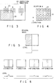
- Inspection image data 20 (FIG. 3) is defined by a plurality of pixel data 21.
- a pattern 22 is defined by the level values of these pixel data 21.
- Each of local areas 23 is defined by 3 ⁇ 3, i.e., a total of nine pixel data 21.
- the local area 23 at a position A is located at an edge portion of the pattern 22.
- the local area 23 at a position B is located at a corner portion of the pattern 22.
- the local area at a position C is located at a uniform portion other than the pattern 22.
- pixel data in the local area 23 at the position A has a smooth density gradation, as shown in FIG. 4.
- This local area 23 consists of 5 ⁇ 5 pixel data. Numerical values of these pixel data indicate multi-value density levels.
- Differential processing for the inspection image data shown in FIG. 4 using a differential operator Db in the y direction shown in FIG. 2B is as follows.
- a differential value in the y direction for each of central density levels "5" corresponds to the difference "4" between two pixel data "7" and “3” adjacent to the density level "5" in the y direction.
- this differential value represents a slope defined by neighboring pixel data in the differential direction, i.e., the y direction.
- the first and second differential circuits 3 and 7 calculate differential values in the above-mentioned four directions in units of pixel data.
- the relationship between a pattern (original image) of image data and the differential values is as follows.
- the original image has an edge in the y direction, as shown in FIG. 5.
- the differential value in the x direction assumes a maximum value
- the differential value in the y direction assumes a minimum value "0", as shown in FIG. 6.
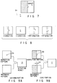
- the original image includes a defect G near the edge, as shown in FIG. 7.
- the defect G projects in the x direction.
- the differential direction in which the differential value largely changes due to the presence of the defect G is the y direction.
- the differential value in the y direction assumes a minimum value.
- the minimum value direction detection circuit 8 receives the differential values (absolute values) in the respective directions from the second differential circuit 7, and detects the differential direction corresponding to the smallest one of the received differential values (the y direction in this case). The circuit 8 supplies the y direction to the selector 4.
- the selector 4 receives the differential values in the four directions from the first differential circuit 3, selects the differential value in the y direction designated by the minimum value direction detection circuit 8 from the received differential values, and sends the differential value in the y direction to a defect judge circuit (discrimination circuit) 9.
- the defect judge circuit 9 compares the input differential value with a predetermined threshold value, and when the differential value exceeds the threshold value, the circuit 9 determines that the pattern defect G is present in the pixel data corresponding to this differential value.
- a direct comparison circuit 10 directly compares pixel data which are not differentiated.
- the direct comparison circuit 10 calculates difference data between each pixel data in the inspection image data and the corresponding pixel data in the reference image data.
- a defect judge circuit 11 compares each of the difference data from the direct comparison circuit 10 with a threshold value. When the difference data exceeds the threshold value, the defect judge circuit 11 determines that a pattern defect is present in this pixel data.
- FIG. 9A shows a differential value for the uniform portion (FIG. 3A) at the position C input to the defect judge circuit 9.
- This uniform portion includes a defect Ga.
- All the differential values, in the respective directions, of the reference image data of this uniform portion are "0" and are equal to each other. For example, a maximum value of differential values in the x and y directions is calculated. Then, the reference pattern is compared with the maximum value. Thus, the defect Ga included in the uniform portion can be clearly detected.
- the position or pattern coordinates of inspection image data and reference image data must be set to perfectly coincide with each other.
- the first and second differential circuits 3 and 7 compare differential values in the respective directions.
- inspection image data and reference image data are shifted by ⁇ t in the x direction, as shown in FIG. 9B.
- the entire area, in the vertical direction, of the width ⁇ t is detected as a pattern defect as a result of defect detection of the direct comparison circuit 10.
- the differential value in the x direction changes at the edge portion of the pattern, but the differential value in the y direction does not change from "0".
- the differential value, in the y direction, of the inspection image data assumes a value corresponding to the defect Gb.
- the defect judge circuit 9 detects a pattern defect from this differential value.
- the differential values in the -45° direction have some small value, and the differential values in the remaining directions has bigger value.
- the minimum differential value directions of the inspection image data and the reference image data with respect to pixel data do not coincide with each other.
- the selector 4 selects the differential value in the differential direction designated by the minimum value direction detection circuit 8
- the selected differential value is not "0" but has a value corresponding to the shift width ⁇ t.
- the defect judge circuit 9 detects a pattern defect.
- the corner portion includes a defect Gd
- the differential value corresponding to this defect Gd is selected by the selector 4.
- the defect judge circuit 9 detects the differential value corresponding to this defect Gd as a pattern defect Ge.
- the pattern defect Ge resulting from the defect Gd is detected in the same manner as the false defect Gc due to the shift width ⁇ t.
- a pattern edge direction in reference image data for pattern defect detection of an object to be inspected is detected, reference image data is differentiated using a differential operator in a direction along the detected pattern edge direction, and inspection image data obtained by scanning an image of the object to be inspected is differentiated using the differential operator in the direction along the detected pattern edge direction.
- the differential data obtained by the differential processing are compared with the inspection image data, and a pattern defect on the object to be inspected is detected on the basis of the difference between these data.
- a pattern defect inspection apparatus comprising: image pickup means for picking up an image of an object to be inspected to generate inspection image data; reference image generation means for generating reference image data for comparing with the inspecting pattern on the object; edge direction detection means for detecting a pattern edge direction in the reference image data; first edge direction differential means for executing differential processing of the inspection image data using a differential operator in a direction along the pattern edge direction; second edge direction differential means for executing differential processing of the reference image data using the differential operator in the direction along the pattern edge direction; differential processing means for executing differential processing of surrounding pixels in the reference image data using the differential operator in the direction along the pattern edge direction, and executing differential processing of the reference image data using differential operators in directions neighboring the pattern edge direction; and discrimination means for detecting a pattern defect of the object to be inspected on the basis of a difference between difference data obtained by the first edge direction differential means, and differential data obtained by the second edge direction differential means or at least one of differential data obtained by the differential processing means.
- inspection image data is generated by scanning an image of an object to be inspected, and reference image data of the object to be inspected is generated.
- a pattern edge direction in the reference image data is detected.
- the inspection image data is differentiated using a differential operator along the detected pattern edge direction, and the reference image data is also differentiated using the differential operator along the detected pattern edge direction.
- surrounding pixels of the reference image data are differentiated using a differential operator in a direction along the pattern edge direction, and are differentiated using differential operators in directions neighboring the pattern edge direction. Then, a pattern defect of the object to be inspected is discriminated on the basis of the difference between the differential value for the inspection image data and at least one differential value of those for the reference image data.
- FIG. 11 is a block diagram showing the arrangement of the pattern defect inspection apparatus.
- the same reference numerals in FIG. 11 denote the same parts as in the pattern defect inspection apparatus shown in FIG. 1. Therefore, a detailed description of repetitive portions will be omitted.
- An image signal output from an image sensor (for instance scan) 1 is converted into multi-value data by an A/D converter 2, and thereafter, the multi-value data is spatially differentiated by a first differential circuit 3 using differential operators in the x, y, and ⁇ 45° directions.
- a design pattern output from a design data memory 5 is converted into reference image data by a reference image generator 6, and thereafter, the reference image data is spatially converted by a second differential circuit 7 using differential operators in the x, y, and ⁇ 45° directions.
- a minimum value direction detection circuit 8 detects a differential direction corresponding to a differential value having the smallest absolute value of the differential values output from the second differential circuit 7, and sends this differential value to first and second selectors 30 and 31.
- the reference image data output from the reference image generator 6 is supplied to a third differential circuit 32.
- the third differential circuit 32 fetches 3 ⁇ 3, i.e., a total of nine pixel data forming a local area including the pixel data of interest at the center.
- the third differential circuit 32 calculates differential values for eight surrounding pixel data other than the central pixel data of the fetched pixel data using the differential operators in the four directions.
- the eight differential values in each direction output from the third differential circuit 32 are input to a maximum value detection circuit 33.
- the maximum value detection circuit 33 detects a maximum differential value, i.e., a differential value having the largest absolute value in each direction from the eight differential values in each direction output from the third differential circuit 32, and supplies these four maximum differential values to the second selector 31.
- the first selector 30 selects a differential value in the differential direction designated by the minimum value direction detection circuit 8 from the differential values in the four directions output from the first differential circuit 3, and supplies the selected value to a subtraction circuit 34.
- the second selector 31 selects a maximum differential value in the differential direction designated by the minimum value direction detection circuit 8 from the four maximum differential values input from the maximum value detection circuit 33, and supplies the selected value to the subtraction circuit 34.
- the subtraction circuit 34 calculates the difference between the differential value from the first selector 30 and the maximum differential value from the second selector 31, and supplies the difference as a difference differential value to a negative value cancel circuit 35.
- the negative value cancel circuit 35 replaces only a negative difference differential value by "0", and supplies the difference differential value to a defect judge circuit 36.
- the defect judge circuit 36 determines that pixel data corresponding to the difference differential value is a pattern defect.
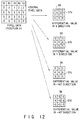
- the first differential circuit 3 fetches, e.g., nine pixel data in the local area 23 including the central pixel data "5" at the center.
- the first differential circuit 3 calculates differential values, in the four directions, of the central pixel data "5".
- the first differential circuit 3 performs spatial differentiation using differential operators Da to Dd in the x, y, and ⁇ 45° directions.
- differential values 37a to 37d, in the four directions, for the central pixel data "5" are respectively "0", "4", "4", and "-4", as shown in FIG. 12.
- the second differential circuit 7 spatially differentiates pixel data of reference image data using the differential operators Da to Dd in the four directions to obtain differential values.
- the absolute values of differential values 37a to 37d at the position A in the reference image data shown in FIG. 12 are respectively “0", "4", "4", and "4".
- the minimum value is "0".
- the minimum value direction detection circuit 8 supplies the x direction corresponding to the differential value 37a having the minimum value "0" to the first and second selectors 30 and 31.
- the third differential circuit 21 calculates differential values 38 in the four directions for each of the eight pixel data spatially differentiated by the second differential circuit 7.
- the differential values in the y direction include six "5"s and two “2"s.
- the differential values in the +45° direction include six "5"s and two "4"s.
- the differential values in the -45° direction include six "-5"s and two "-4"s.
- the maximum differential value selected by the second selector 31 is "0" shown in FIG. 13A.
- the first selector 30 selects the value "0" of the differential value 37a in the x direction for the central pixel data "5".
- the subtraction circuit 34 outputs a difference differential value "0".
- the defect judge circuit 36 does not detect any pattern defect, as a matter of course.
- FIG. 13B shows the processing result for central pixel data "6" in a corner portion at a position B.
- the minimum value direction of the differential values in the four directions of the pixel data "6" is the -45° direction.
- a differential value of pixel data in the -45° direction becomes “0"
- eight differential values in the -45° direction of surrounding pixel data include values "4", "3", "2", and "0". Therefore, the maximum value is "4".
- the defect judge circuit 36 does not detect any pattern defect.
- FIG. 13C shows the processing result for central pixel data "0" in a uniform portion at a position C. In this case as well, no pattern defect is output.
- the minimum value direction detection circuit 8 detects the x direction for the edge portion at the position A shown in FIG. 3.
- the subtraction circuit 34 receives a differential value "0" in the x direction from the first differential circuit 3.
- central pixel data in the reference image data does not correspond to the central pixel data in the inspection image data, and is shifted by one pixel from it.
- the minimum value direction detection circuit 8 does not always designate the -45° differential direction. Therefore, the first selector 30 does not always select the differential value "0" in the -45° direction.
- the minimum value direction detection circuit 8 detects a value at least larger than the differential value output from the first selector 30.
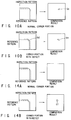
- the subtraction circuit 34 calculates the difference between the values from the selectors 30 and 31. With this calculation, the differential value output from the first selector 30 is canceled. Therefore, no defect is output, as shown in FIG. 14A.
- the first differential circuit 3 differentiates inspection image data, and outputs a differential value in the x direction corresponding to the defect.
- the second differential circuit 7 outputs a differential value "0" in the x direction of surrounding pixel data around the central pixel data.
- the subtraction circuit 34 outputs a difference differential value corresponding to the defect scale.
- the defect judge circuit 36 outputs a pattern defect.
- the differential direction designated by the minimum value direction detection circuit 8 for the local area 23 of the corner portion at the position B, is not uniquely determined.
- the first differential circuit 3 outputs differential values corresponding to the defect in the respective differential direction including the -45° direction.
- the first selector 30 selects a differential value corresponding to the defect.
- the subtraction circuit 34 detects a defect Gf, as shown in FIG. 14B.
- the defect Gf can be prevented from including a pseudo defect Gc caused by the shift, and only an actual defect can be reliably detected with high accuracy.
- FIG. 15 is a block diagram showing the arrangement of a pattern defect detection apparatus.
- An image sensor 40 comprises a line sensor.
- the image sensor 40 is connected to a plural direction differential circuit 42 via an A/D converter 41.
- the plural direction differential circuit 42 has differential operators in the x, y, +45°, and -45° directions, and has a function of executing differential processing of inspection image data using these differential operators.
- this plural direction differential circuit 42 has differential operators in +22.5°, +67.5°, -22.5°, and -67.5° directions shown in FIG. 16 in addition to the above-mentioned differential operators.
- the plural direction differential circuit 42 has a function of executing differential processing of inspection image data in the four or eight directions of these differential operators.
- a maximum value direction detection circuit 43 has a function of receiving processing results in the respective differential directions from the plural direction differential circuit 42, detecting the differential direction of a differential value having a maximum value from the received differential values (absolute values) in the respective differential directions, and supplying the detected differential direction to a selector 44.
- a reference data generation circuit 45 has a function of generating reference image data corresponding to inspection image data obtained by an image pickup operation of the image sensor on the basis of design data of pattern data in synchronism with position data.
- An edge direction detection circuit 46 has a function of detecting edge directions of the pattern in the reference image data in units of pixels, and supplying the detection results to the selector 44.
- the edge direction detection circuit 46 When the pattern edge direction is indefinite, the edge direction detection circuit 46 has a function of sending a message indicating that the direction is indefinite to the selector 44.
- the selector 44 has a function of normally selecting the differential direction detected by the edge direction detection circuit 46 as a pattern edge direction, and selecting the differential direction detected by the maximum value direction detection circuit 43 upon reception of a message indicating that the direction is indefinite.
- a first edge direction differential circuit 47 has a function of receiving the differential direction as the pattern edge direction selected by the selector 44, and executing differential processing of inspection image data from the A/D converter 41 using the received differential direction so as to calculate the absolute value of the differential value.
- a second edge direction differential circuit 48 has a function of receiving the differential direction as the pattern edge direction selected by the selector 44, and executing differential processing of reference image data using the received differential direction so as to calculate the absolute value of the differential value.
- a differential processing means 50 has a function of executing differential processing of surrounding pixels of the reference image data using differential operators in a direction along the pattern edge direction.
- the differential processing means 50 has a function of executing differential processing of the reference image data using differential operators in directions neighboring to the pattern edge direction.
- the differential processing means 50 has functions of a surrounding pixel edge direction differential circuit 51, a first maximum value detection circuit 52, a neighboring direction differential circuit 53, and a second maximum value detection circuit 54.
- the surrounding pixel edge direction differential circuit 51 has a function of executing differential processing of reference image data for surrounding pixels around a pixel, for which a differential value is to be calculated, using differential operators in a direction along the pattern edge direction detected by the edge direction detection circuit 46.
- the first maximum value detection circuit 52 has a function of detecting a maximum absolute value from the differential values of the surrounding pixels calculated by the surrounding pixel edge direction differential circuit 51.
- the neighboring direction differential circuit 53 has a function of executing differential processing of reference image data using differential operators in directions neighboring the pattern edge direction detected by the edge direction detection circuit 46.
- the neighboring direction differential circuit 53 has a function of executing differential processing of reference image data using differential operators in the x and y directions which are orthogonal to each other, and the ⁇ 45°, ⁇ 22.5°, and ⁇ 67.5° directions with respect to the x direction.
- the second maximum value detection circuit 54 has a function of detecting a maximum value from the absolute values of the differential values calculated by the neighboring direction differential circuit 53.
- the output terminals of the edge direction differential circuit 48 and the first and second maximum value detection circuits 52 and 54 are connected to a subtraction circuit 56 via a select switch 55.
- the subtraction circuit 56 has a function of calculating the differences, in units of pixels, between the inspection image data differentiated by the edge direction differential circuit 47, and differential data from one of the edge direction differential circuit 48, and the first and second maximum value detection circuits 52 and 54, which is selected by the select switch 55.
- a defect judge circuit 57 has a function of comparing difference values in units of pixels from the subtraction circuit 56 with a predetermined threshold value, and determining, to be a defect, a pixel corresponding to the difference value in units of pixels, which exceeds the threshold value.
- the reference data generation circuit 45 generates reference image data on the basis of design data of pattern data.
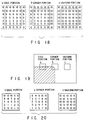
- FIG. 17 is a view showing the reference image data. Local areas, edge, corner, and uniform portions a , b, and c are set. Each of these edge, corner, and uniform portions a , b, and c is defined by 7 ⁇ 7 pixels, as shown in FIG. 18. In each of the edge, corner, and uniform portions a , b, and c, a dark portion is indicated by a density level "0", and a light portion is indicated by a density level "10".
- the reference image data is data generated based on the design data, and has smooth density gradation at an edge.
- the image sensor 40 continuously picks up an image of an object to be inspected, and outputs its image signal.
- the image signal is converted into digital inspection image data corresponding to 11 density levels by the A/D converter 41.
- FIG. 19 is a view showing inspection image data without a defect.
- Each of the edge, corner, and uniform portions a , b, and c in the inspection image data is defined by 5 ⁇ 5 pixels, as shown in FIG. 20.
- FIG. 21 is a view showing inspection image data with a defect.
- Each of the edge, corner, and uniform portions a , b, and c in the inspection image data is defined by 5 ⁇ 5 pixels, as shown in FIG. 22.
- Image data of each corner portion b in these inspection image data is shifted by one pixel from image data of the corner portion b shown in FIG. 18 in the -y direction.
- the reference image data is supplied to the edge direction detection circuit 46.
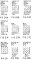
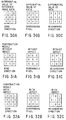
- the edge direction detection circuit 46 performs differential processing of the reference image data in the x, y, +45°, and -45° directions, and detects the differential direction of a minimum differential value from the calculated differential values.
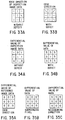
- the edge direction detection circuit 46 detects pattern edge directions in the uniform portion c in the reference image data, as shown in FIG. 33A. In this case, since the density level is uniform, the direction becomes indefinite.
- the edge direction detection circuit 46 detects pattern edge directions in the uniform portion c in the reference image data, as shown in FIG. 33B.
- the plural direction differential circuit 42 executes differential processing of inspection image data using differential operators in the x, y, +45°, and -45° directions.
- the selector 44 selects a differential direction exhibiting a maximum value from the differential values in the edge directions detected by the maximum value direction detection circuit 43.
- the first edge direction differential circuit 47 executes differential processing of the inspection image data using the differential operators in the detected differential direction.
- the second edge direction differential circuit 48, the surrounding pixel edge direction differential circuit 51, and the neighboring direction differential circuit 53 respectively execute differential processing of reference image data in accordance with the selected edge directions.
- the subtraction results of the subtraction circuit 56 become the same as the differential values of the inspection image data, as shown in FIGS. 36 and 37.
- the defect judge circuit 57 discriminates a pattern defect by comparing the subtraction results from the subtraction circuit 56 with a threshold value.
- a pattern defect can be reliably detected by comparing the reference and inspection image data.
- the apparatus since the apparatus has a function of detecting a maximum value by executing differential processing of the reference image data for each pixel and surrounding pixels around the pixel, and detecting a maximum value by executing differential processing of the reference image data in the edge direction and in directions neighboring the edge direction, even when the edge, corner, and uniform portions a , b, and c suffer a coordinate position shift from the pattern, a pattern defect can be detected with high accuracy in these portions.
- the subtraction circuit 56 may calculate the difference between the inspection image data differentiated by the first edge direction differential circuit 47 and differential image data obtained from at least one of the second edge direction differential circuit 48, the surrounding pixel edge direction differential processing circuit 51, and the neighboring direction differential circuit 53.
- differential operators differential values in the x, y, and ⁇ 45° directions may be obtained using Sobel operators, as shown in, e.g., FIGS. 38A to 38D.
Landscapes
- Physics & Mathematics (AREA)
- General Physics & Mathematics (AREA)
- General Health & Medical Sciences (AREA)
- Chemical & Material Sciences (AREA)
- Analytical Chemistry (AREA)
- Biochemistry (AREA)
- Life Sciences & Earth Sciences (AREA)
- Health & Medical Sciences (AREA)
- Immunology (AREA)
- Pathology (AREA)
- Investigating Materials By The Use Of Optical Means Adapted For Particular Applications (AREA)
- Testing Or Measuring Of Semiconductors Or The Like (AREA)
- Length Measuring Devices By Optical Means (AREA)
- Image Analysis (AREA)
- Image Processing (AREA)
Applications Claiming Priority (2)
| Application Number | Priority Date | Filing Date | Title |
|---|---|---|---|
| JP5209453A JPH0763691A (ja) | 1993-08-24 | 1993-08-24 | パターン欠陥検査方法及びその装置 |
| JP209453/93 | 1993-08-24 |
Publications (1)
| Publication Number | Publication Date |
|---|---|
| EP0643293A1 true EP0643293A1 (de) | 1995-03-15 |
Family
ID=16573129
Family Applications (1)
| Application Number | Title | Priority Date | Filing Date |
|---|---|---|---|
| EP94113243A Ceased EP0643293A1 (de) | 1993-08-24 | 1994-08-24 | Verfahren und Vorrichtung zur Erkennung von Musterfehlern |
Country Status (4)
| Country | Link |
|---|---|
| US (1) | US5574800A (de) |
| EP (1) | EP0643293A1 (de) |
| JP (1) | JPH0763691A (de) |
| KR (1) | KR0143948B1 (de) |
Cited By (5)
| Publication number | Priority date | Publication date | Assignee | Title |
|---|---|---|---|---|
| WO1999017102A1 (en) * | 1997-09-30 | 1999-04-08 | Siemens Aktiengesellschaft | A method of and apparatus for inspecting printed information |
| EP1347286A1 (de) * | 2002-03-19 | 2003-09-24 | Siemens Aktiengesellschaft | Verfahren und Vorrichtung zur Kontrolle von Objekten |
| EP1400922A1 (de) * | 2002-09-20 | 2004-03-24 | Nitto Denko Corporation | Vorrichtung und Verfahren zum Überprüfen von Abdrücken |
| EP1626270A4 (de) * | 2003-05-16 | 2008-02-13 | Topcon Corp | Inspektionsverfahren mit betrachtung von aussen, dafür verwendete mustervorlage sowie die mustervorlage aufweisende inspektionsvorrichtung mit betrachtung von aussen |
| CN104765663A (zh) * | 2014-01-03 | 2015-07-08 | 神讯电脑(昆山)有限公司 | 外观检测自动测试方法 |
Families Citing this family (35)
| Publication number | Priority date | Publication date | Assignee | Title |
|---|---|---|---|---|
| JPH0821804A (ja) * | 1994-07-08 | 1996-01-23 | Rohm Co Ltd | ワイヤ切れ検出方法 |
| JP3659426B2 (ja) * | 1994-09-02 | 2005-06-15 | ソニー株式会社 | エツジ検出方法及びエツジ検出装置 |
| JP3794502B2 (ja) | 1994-11-29 | 2006-07-05 | ソニー株式会社 | 画像領域抽出方法及び画像領域抽出装置 |
| JP2999679B2 (ja) * | 1994-11-30 | 2000-01-17 | 大日本スクリーン製造株式会社 | パターン欠陥検査装置 |
| JPH09128529A (ja) * | 1995-10-30 | 1997-05-16 | Sony Corp | ディジタル画像の雑音の投影に基づく除去方法 |
| JP3994445B2 (ja) * | 1995-12-05 | 2007-10-17 | ソニー株式会社 | 動きベクトル検出装置及び動きベクトル検出方法 |
| JP3418497B2 (ja) * | 1996-04-16 | 2003-06-23 | 松下電器産業株式会社 | 部品認識方法 |
| TW357327B (en) * | 1996-08-02 | 1999-05-01 | Sony Corp | Methods, apparatus and program storage device for removing scratch or wire noise, and recording media therefor |
| US5912988A (en) * | 1996-12-27 | 1999-06-15 | Xytec Corporation | Image processing method and apparatus for distortion compensation |
| US6078616A (en) | 1997-03-13 | 2000-06-20 | Sony Corporation | Methods and apparatus for error concealment utilizing temporal domain motion vector estimation |
| US6400838B2 (en) * | 1997-07-29 | 2002-06-04 | Kabushiki Kaisha Toshiba | Pattern inspection equipment, pattern inspection method, and storage medium storing pattern inspection program |
| US5999636A (en) * | 1997-10-10 | 1999-12-07 | Printprobe Technology, Llc | Apparatus and process for inspecting print material |
| US6229578B1 (en) * | 1997-12-08 | 2001-05-08 | Intel Corporation | Edge-detection based noise removal algorithm |
| JP3120767B2 (ja) * | 1998-01-16 | 2000-12-25 | 日本電気株式会社 | 外観検査装置、外観検査方法及び外観検査プログラムを記録した記録媒体 |
| EP1061330A1 (de) * | 1998-11-30 | 2000-12-20 | Olympus Optical Co., Ltd. | Fehlstellendetektor |
| JP2000241117A (ja) * | 1999-02-22 | 2000-09-08 | Keyence Corp | 画像のエッジ検出方法、検査装置及び記録媒体 |
| JP4017285B2 (ja) * | 1999-06-02 | 2007-12-05 | 松下電器産業株式会社 | パターン欠陥検出方法 |
| US7796801B2 (en) * | 1999-08-26 | 2010-09-14 | Nanogeometry Research Inc. | Pattern inspection apparatus and method |
| US7817844B2 (en) * | 1999-08-26 | 2010-10-19 | Nanogeometry Research Inc. | Pattern inspection apparatus and method |
| JP2002162729A (ja) | 2000-11-24 | 2002-06-07 | Toshiba Corp | パターン検査方法、パターン検査装置およびマスクの製造方法 |
| JP2002310929A (ja) * | 2001-04-13 | 2002-10-23 | Mitsubishi Electric Corp | 欠陥検査装置 |
| US20030131350A1 (en) * | 2002-01-08 | 2003-07-10 | Peiffer John C. | Method and apparatus for identifying a digital audio signal |
| US7155052B2 (en) * | 2002-06-10 | 2006-12-26 | Tokyo Seimitsu (Israel) Ltd | Method for pattern inspection |
| US7463765B2 (en) * | 2003-02-25 | 2008-12-09 | Lamda-Lite Enterprises Incorporated | System and method for detecting and reporting fabrication defects using a multi-variant image analysis |
| JP4351522B2 (ja) * | 2003-11-28 | 2009-10-28 | 株式会社日立ハイテクノロジーズ | パターン欠陥検査装置およびパターン欠陥検査方法 |
| JP4018642B2 (ja) * | 2004-01-05 | 2007-12-05 | 株式会社東芝 | 参照データ生成方法、パターン欠陥検査装置、パターン欠陥検査方法、及び参照データ生成プログラム |
| US7620241B2 (en) * | 2004-11-30 | 2009-11-17 | Hewlett-Packard Development Company, L.P. | Artifact reduction in a digital video |
| JP4644210B2 (ja) * | 2005-01-14 | 2011-03-02 | 富士通セミコンダクター株式会社 | パターン欠陥検査方法 |
| KR100684102B1 (ko) * | 2005-06-30 | 2007-02-16 | 삼성전자주식회사 | 결함 검사 방법 및 이를 이용한 결함 검사 장치 |
| JP4174504B2 (ja) * | 2005-08-31 | 2008-11-05 | アドバンスド・マスク・インスペクション・テクノロジー株式会社 | 試料検査装置、試料検査方法及びプログラム |
| JP4871144B2 (ja) * | 2006-01-13 | 2012-02-08 | 株式会社東芝 | 画像処理装置、方法、プログラム |
| US7369236B1 (en) * | 2006-10-31 | 2008-05-06 | Negevtech, Ltd. | Defect detection through image comparison using relative measures |
| JP5429869B2 (ja) * | 2008-12-22 | 2014-02-26 | 株式会社 Ngr | パターン検査装置および方法 |
| US8150140B2 (en) * | 2008-12-22 | 2012-04-03 | Ngr Inc. | System and method for a semiconductor lithographic process control using statistical information in defect identification |
| JP6546826B2 (ja) * | 2015-10-08 | 2019-07-17 | 株式会社日立パワーソリューションズ | 欠陥検査方法、及びその装置 |
Citations (5)
| Publication number | Priority date | Publication date | Assignee | Title |
|---|---|---|---|---|
| GB2102122A (en) * | 1981-07-22 | 1983-01-26 | Nat Res Dev | Detecting defects in a pattern |
| US4532650A (en) * | 1983-05-12 | 1985-07-30 | Kla Instruments Corporation | Photomask inspection apparatus and method using corner comparator defect detection algorithm |
| US4958374A (en) * | 1988-03-04 | 1990-09-18 | Toshiba Machine Company, Ltd. | Method of checking pattern and apparatus therefor |
| US5157735A (en) * | 1988-09-09 | 1992-10-20 | Hitachi, Ltd. | Chipping detection system and method |
| US5185812A (en) * | 1990-02-14 | 1993-02-09 | Kabushiki Kaisha Toshiba | Optical pattern inspection system |
Family Cites Families (5)
| Publication number | Priority date | Publication date | Assignee | Title |
|---|---|---|---|---|
| JP2504951B2 (ja) * | 1986-05-15 | 1996-06-05 | 東芝機械株式会社 | パタ−ン検査方法 |
| US4805123B1 (en) * | 1986-07-14 | 1998-10-13 | Kla Instr Corp | Automatic photomask and reticle inspection method and apparatus including improved defect detector and alignment sub-systems |
| JP3132565B2 (ja) * | 1989-08-30 | 2001-02-05 | 株式会社日立製作所 | 欠陥検査方法及びその装置 |
| JPH0722173B2 (ja) * | 1990-04-10 | 1995-03-08 | 株式会社東芝 | パターン欠陥検査装置 |
| JP2533245B2 (ja) * | 1991-03-28 | 1996-09-11 | 株式会社東芝 | パタ―ン欠陥検査装置 |
-
1993
- 1993-08-24 JP JP5209453A patent/JPH0763691A/ja active Pending
-
1994
- 1994-08-23 KR KR1019940020758A patent/KR0143948B1/ko not_active Expired - Fee Related
- 1994-08-23 US US08/294,510 patent/US5574800A/en not_active Expired - Fee Related
- 1994-08-24 EP EP94113243A patent/EP0643293A1/de not_active Ceased
Patent Citations (5)
| Publication number | Priority date | Publication date | Assignee | Title |
|---|---|---|---|---|
| GB2102122A (en) * | 1981-07-22 | 1983-01-26 | Nat Res Dev | Detecting defects in a pattern |
| US4532650A (en) * | 1983-05-12 | 1985-07-30 | Kla Instruments Corporation | Photomask inspection apparatus and method using corner comparator defect detection algorithm |
| US4958374A (en) * | 1988-03-04 | 1990-09-18 | Toshiba Machine Company, Ltd. | Method of checking pattern and apparatus therefor |
| US5157735A (en) * | 1988-09-09 | 1992-10-20 | Hitachi, Ltd. | Chipping detection system and method |
| US5185812A (en) * | 1990-02-14 | 1993-02-09 | Kabushiki Kaisha Toshiba | Optical pattern inspection system |
Cited By (9)
| Publication number | Priority date | Publication date | Assignee | Title |
|---|---|---|---|---|
| WO1999017102A1 (en) * | 1997-09-30 | 1999-04-08 | Siemens Aktiengesellschaft | A method of and apparatus for inspecting printed information |
| EP1347286A1 (de) * | 2002-03-19 | 2003-09-24 | Siemens Aktiengesellschaft | Verfahren und Vorrichtung zur Kontrolle von Objekten |
| EP1400922A1 (de) * | 2002-09-20 | 2004-03-24 | Nitto Denko Corporation | Vorrichtung und Verfahren zum Überprüfen von Abdrücken |
| US7260244B2 (en) | 2002-09-20 | 2007-08-21 | Nitto Denko Corporation | Print inspection method and print inspection apparatus |
| EP1626270A4 (de) * | 2003-05-16 | 2008-02-13 | Topcon Corp | Inspektionsverfahren mit betrachtung von aussen, dafür verwendete mustervorlage sowie die mustervorlage aufweisende inspektionsvorrichtung mit betrachtung von aussen |
| CN100483118C (zh) * | 2003-05-16 | 2009-04-29 | 株式会社拓普康 | 外观检测方法,标准图案及具有标准图案的外观检查装置 |
| US7822262B2 (en) | 2003-05-16 | 2010-10-26 | Kabushiki Kaisha Topcon | Outer surface-inspecting method, master patterns used therefor, and outer surface-inspecting apparatus equipped with such a master pattern |
| CN104765663A (zh) * | 2014-01-03 | 2015-07-08 | 神讯电脑(昆山)有限公司 | 外观检测自动测试方法 |
| CN104765663B (zh) * | 2014-01-03 | 2018-02-27 | 神讯电脑(昆山)有限公司 | 外观检测自动测试方法 |
Also Published As
| Publication number | Publication date |
|---|---|
| KR950006428A (ko) | 1995-03-21 |
| US5574800A (en) | 1996-11-12 |
| KR0143948B1 (ko) | 1998-07-15 |
| JPH0763691A (ja) | 1995-03-10 |
Similar Documents
| Publication | Publication Date | Title |
|---|---|---|
| US5574800A (en) | Pattern defect inspection method and apparatus | |
| US6347150B1 (en) | Method and system for inspecting a pattern | |
| US20060018534A1 (en) | Technique for detecting a defect of an object by area segmentation of a color image of the object | |
| US20030031356A1 (en) | Pattern inspection apparatus and method | |
| KR20090101356A (ko) | 결함 검출 장치 및 결함 검출 방법 | |
| JP2007071586A (ja) | 画像欠陥検査装置、画像欠陥検査システム、欠陥分類装置及び画像欠陥検査方法 | |
| US5384711A (en) | Method of and apparatus for inspecting pattern on printed board | |
| KR19990083445A (ko) | 시각검사장치및방법 | |
| JP2533245B2 (ja) | パタ―ン欠陥検査装置 | |
| US5416335A (en) | Automated visual inspection system for determining the set positions of a row of dip switches | |
| JP3836988B2 (ja) | パターン検査方法およびパターン検査装置 | |
| JP4827896B2 (ja) | 画像欠陥検査方法、画像欠陥検査装置及び外観検査装置 | |
| West et al. | The automatic visual inspection of printed circuit boards | |
| JP3198105B2 (ja) | 自動外観検査装置 | |
| JP2912070B2 (ja) | 対象物の位置認識方法 | |
| JPH02150704A (ja) | 物体検査装置 | |
| JP2658594B2 (ja) | 表面実装icリードずれ検査装置 | |
| JPH03278195A (ja) | 枚数測定装置 | |
| JPH0722173B2 (ja) | パターン欠陥検査装置 | |
| JPH0763692A (ja) | パターン欠陥検査方法及びその装置 | |
| JPH05126754A (ja) | パターン欠陥検査装置 | |
| JPH0359362B2 (de) | ||
| JPH0721372A (ja) | 画像検出装置 | |
| JPH04310852A (ja) | 微小欠陥検出装置 | |
| JPH08159980A (ja) | 外観検査装置の対象面認識処理方式 |
Legal Events
| Date | Code | Title | Description |
|---|---|---|---|
| PUAI | Public reference made under article 153(3) epc to a published international application that has entered the european phase |
Free format text: ORIGINAL CODE: 0009012 |
|
| 17P | Request for examination filed |
Effective date: 19940921 |
|
| AK | Designated contracting states |
Kind code of ref document: A1 Designated state(s): DE GB |
|
| 17Q | First examination report despatched |
Effective date: 20020311 |
|
| STAA | Information on the status of an ep patent application or granted ep patent |
Free format text: STATUS: THE APPLICATION HAS BEEN REFUSED |
|
| 18R | Application refused |
Effective date: 20080525 |