EP0645826A2 - Monolithischer Optokoppler mit mehreren Kanälen - Google Patents
Monolithischer Optokoppler mit mehreren Kanälen Download PDFInfo
- Publication number
- EP0645826A2 EP0645826A2 EP94114455A EP94114455A EP0645826A2 EP 0645826 A2 EP0645826 A2 EP 0645826A2 EP 94114455 A EP94114455 A EP 94114455A EP 94114455 A EP94114455 A EP 94114455A EP 0645826 A2 EP0645826 A2 EP 0645826A2
- Authority
- EP
- European Patent Office
- Prior art keywords
- set forth
- light
- coupler
- photodetectors
- common
- Prior art date
- Legal status (The legal status is an assumption and is not a legal conclusion. Google has not performed a legal analysis and makes no representation as to the accuracy of the status listed.)
- Ceased
Links
Images
Classifications
-
- H—ELECTRICITY
- H10—SEMICONDUCTOR DEVICES; ELECTRIC SOLID-STATE DEVICES NOT OTHERWISE PROVIDED FOR
- H10F—INORGANIC SEMICONDUCTOR DEVICES SENSITIVE TO INFRARED RADIATION, LIGHT, ELECTROMAGNETIC RADIATION OF SHORTER WAVELENGTH OR CORPUSCULAR RADIATION
- H10F55/00—Radiation-sensitive semiconductor devices covered by groups H10F10/00, H10F19/00 or H10F30/00 being structurally associated with electric light sources and electrically or optically coupled thereto
- H10F55/20—Radiation-sensitive semiconductor devices covered by groups H10F10/00, H10F19/00 or H10F30/00 being structurally associated with electric light sources and electrically or optically coupled thereto wherein the electric light source controls the radiation-sensitive semiconductor devices, e.g. optocouplers
- H10F55/25—Radiation-sensitive semiconductor devices covered by groups H10F10/00, H10F19/00 or H10F30/00 being structurally associated with electric light sources and electrically or optically coupled thereto wherein the electric light source controls the radiation-sensitive semiconductor devices, e.g. optocouplers wherein the radiation-sensitive devices and the electric light source are all semiconductor devices
- H10F55/255—Radiation-sensitive semiconductor devices covered by groups H10F10/00, H10F19/00 or H10F30/00 being structurally associated with electric light sources and electrically or optically coupled thereto wherein the electric light source controls the radiation-sensitive semiconductor devices, e.g. optocouplers wherein the radiation-sensitive devices and the electric light source are all semiconductor devices formed in, or on, a common substrate
-
- H—ELECTRICITY
- H10—SEMICONDUCTOR DEVICES; ELECTRIC SOLID-STATE DEVICES NOT OTHERWISE PROVIDED FOR
- H10F—INORGANIC SEMICONDUCTOR DEVICES SENSITIVE TO INFRARED RADIATION, LIGHT, ELECTROMAGNETIC RADIATION OF SHORTER WAVELENGTH OR CORPUSCULAR RADIATION
- H10F77/00—Constructional details of devices covered by this subclass
- H10F77/30—Coatings
- H10F77/306—Coatings for devices having potential barriers
- H10F77/331—Coatings for devices having potential barriers for filtering or shielding light, e.g. multicolour filters for photodetectors
- H10F77/334—Coatings for devices having potential barriers for filtering or shielding light, e.g. multicolour filters for photodetectors for shielding light, e.g. light blocking layers or cold shields for infrared detectors
Definitions
- This invention generally relates to optical couplers. Specifically, the invention is directed to a monolithic multiple channel optical coupler.
- Existing optical couplers generally exhibit a variation in performance from device to device. For example, the current transfer ratio and speed of an optical device can vary significantly. This can pose a significant problem when one is coupling multiple channels and minimal device-to-device variation is needed to preserve relative channel signal levels.
- Couplers Part of the problem can be minimized by using multiple channel couplers.
- the individual optical devices within such couplers may be fabricated from different wafers or different portions of the same wafer, they are not necessarily matched devices. Further, such couplers may not use isolated optical paths for the devices to minimize cross-talk. Thus, even within one package, performance variations persist.
- coupler that can handle multiple signals with minimal channel-to-channel variation in signal transfer performance. Also, it is desirable to provide a coupler that has the maximum number of isolated channels using the least number of pins, to reduce assembly costs and to reduce the required printed circuit board space.
- a monolithic-detector, multiple-channel optical coupler having common LED-emitter cathodes and common photodetector collectors, or having common LED-emitter anodes and common photodetector emitters.
- the photodetectors are contained on a single, monolithic substrate which provides substantially-matched devices and common connections for the devices. Although the individual coupling devices share electrical commonality, they are optically isolated by the use of a light pipe arrangement between the LED-emitters and the photodetectors. Moreover, pin count is minimized by using common connections for the LED-emitters and the photodetectors.
- the emitters and photodetectors described here are of the kind discussed in the Siemens Optoelectronics Data Book 1993. It should be understood that other devices can be used as well. Also, the coupler could be used with other types of electromagnetic radiation, such as ultraviolet light.
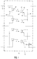
- a monolithic-detector, multiple-channel optical coupler 10 is shown in the electrical schematic diagram of Figure 1.
- the coupler 10 shown here is contained in a dual in-line package 12 having ten pins 14, but could be held in any other suitable packaging device.
- the coupler 10 has four gallium arsenide LED (light emitting diode) emitters 20 (or some other suitable emitter), each having an anode 22 and a cathode 24 with the cathodes 24 tied to a first common bus 26, and four photodetectors 40, each having a collector 42, an emitter 44, and a base 46, with the collectors 42 tied to a second common bus 48.
- Each LED-emitter 20 / photodetector 40 pair is used to couple one signal channel for the coupler 10.
- the number four is arbitrary; any number of devices could be provided. Also, one could commonly connect the anodes 22 of the LED emitters 20 instead of the cathodes 24 and similarly connect the emitters 44 instead of the collectors 42 of the photodetectors 40. Moreover, one could use photodiodes instead of the depicted phototransistors for the photodetectors 40. Finally, if the application required it, one could choose to bring out from the package 12 individual leads for every device, i.e., every LED emitter and photodetector.
- the anodes 22 of the LED emitters 20 and the emitters 44 of the photodetectors 40 are each connected to individual pins 14.
- the common buses 26 and 48 for the cathodes 24 and the collectors 42, respectively, are also connected to separate pins 14 of the package 12.
- individual cathode 24 and/or collector 42 connections could be provided.
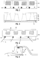
- FIG. 2 The physical structure of the coupler 10 is illustrated in Figures 2 through 5.
- a monolithic substrate 60 having four photodetectors 40 is shown.
- a photodetector region 62 for each photodetector 40 and connecting pads 64 for each associated emitter 44 is visible in this view. Because the four devices come from adjacent portions of the same wafer and their characteristics are thus nearly the same, this arrangement offers nearest neighbor matching of performance or operating characteristics.
- a front-elevation partial assembly view of the coupler 10 is shown in Figure 3.
- the substrate 60 is located on a mounting base 70.
- An opaque shield 80 fabricated from an opaque material, for example, white Lexan®, is positioned over the substrate 60. White is preferable because it reflects light.
- Within the shield 80 are formed respective light pipes 90 for the passage of light to the photodetector regions 62.
- the light pipes 90 have an inward taper 92 from the substrate 60 upwards to minimize cross talk between the channels formed thereby.
- FIG 4 A top partial-assembly view of the coupler 10 is shown in Figure 4.
- electrically-conductive wires 110 connected to the pads 64 for the emitters 44 of the photodetectors 40.
- the wires 110 are each connected to individual pins 14 of the coupler package 12.
- an electrically-conductive wire 120 is shown connected to the anode 22 of an LED emitter 20. Similar wires 120 are connected to the anodes 22 of the other LED emitters 20. As indicated above, the wires 120 are each connected to individual pins 14 of the coupler package 12. Note that the LED emitter 20 is positioned at the tapered end of the light pipe 90 and opposite the respective photodetector region 62. The other LED emitters 20 are similarly positioned at the other light pipes 90 so that each LED emitter 20 is paired with a respective photodetector region 62 via an individual light pipe 90.
- the coupler 10 In actual manufacture of the coupler 10, one could choose to use a detector strip or sheet die attached in one operation on a common lead frame pad or with individual lead frame connections. Also, the individual photodetector region 62/emitter 44 pairs need not be arranged in a line but could be configured in a square or any other desired arrangement that provides substantially matched photodetectors 60.
- the optical coupler 10 is used to transmit signal information between respective circuitry while maintaining electrical isolation therebetween. This is accomplished since optical signals, and not electrical signals, are passed between the LED-emitters 20 and the photodetectors 40 which are connected to respective portions of the circuitry.
- the common collector arrangement of the photodetectors 40 results in a non-inverting amplification of the optical signal received from the LED-emitters 20.
- the light emitted to the respective photodetector 40 will cause the output of the photodetector 40 to be at a high voltage level.
- the output of the photodetector 40 is connected to the remainder of the circuitry.
- the output of the photodetector 40 will be at a low voltage level.
- the light pipes 90 ensure that the light pathway between a respective LED emitter 20 and photodetector 40 is isolated from the other light pathways. As a result, no mixing of optical signals occurs (i.e., no cross talk occurs) and each photodetector 40 receives only one optical signal. Note that, in data communications applications, all signals can be referenced to a common ground on either side of the isolation barrier.
- the coupler 10 achieves an improved channel density per pin count by the use of the common connections of the LED emitters 20 and the photodetectors 40 in lieu of bringing out separate leads for each device.
- the number of pins required for the common connections is two plus twice the number of channels to be coupled.
- the number of required pins equals ten. This is in contrast to presently available four-channel couplers that require sixteen pins and, thus, a much larger package.
- the coupler 10 achieves this improvement in pin count and packaging while increasing performance.
Landscapes
- Photo Coupler, Interrupter, Optical-To-Optical Conversion Devices (AREA)
Applications Claiming Priority (2)
| Application Number | Priority Date | Filing Date | Title |
|---|---|---|---|
| US12594593A | 1993-09-23 | 1993-09-23 | |
| US125945 | 1993-09-23 |
Publications (2)
| Publication Number | Publication Date |
|---|---|
| EP0645826A2 true EP0645826A2 (de) | 1995-03-29 |
| EP0645826A3 EP0645826A3 (de) | 1995-05-17 |
Family
ID=22422179
Family Applications (1)
| Application Number | Title | Priority Date | Filing Date |
|---|---|---|---|
| EP94114455A Ceased EP0645826A3 (de) | 1993-09-23 | 1994-09-14 | Monolithischer Optokoppler mit mehreren Kanälen. |
Country Status (2)
| Country | Link |
|---|---|
| US (1) | US5883395A (de) |
| EP (1) | EP0645826A3 (de) |
Families Citing this family (6)
| Publication number | Priority date | Publication date | Assignee | Title |
|---|---|---|---|---|
| US6093938A (en) * | 1999-05-25 | 2000-07-25 | Intel Corporation | Stacked die integrated circuit device |
| JP2004320135A (ja) * | 2003-04-11 | 2004-11-11 | Sharp Corp | 多チャンネル型光結合装置 |
| US7217041B2 (en) * | 2005-09-26 | 2007-05-15 | Mitutoyo Corporation | Fiber-optic alignment with detector IC |
| DE102007012115A1 (de) | 2006-11-30 | 2008-06-05 | Osram Opto Semiconductors Gmbh | Strahlungsdetektor |
| US20130278064A1 (en) * | 2011-10-19 | 2013-10-24 | Creative Electron, Inc. | Ultra-Low Noise, High Voltage, Adjustable DC-DC Converter Using Photoelectric Effect |
| JP6402091B2 (ja) * | 2015-12-17 | 2018-10-10 | 株式会社東芝 | 光結合装置 |
Family Cites Families (14)
| Publication number | Priority date | Publication date | Assignee | Title |
|---|---|---|---|---|
| DE1264513C2 (de) * | 1963-11-29 | 1973-01-25 | Texas Instruments Inc | Bezugspotentialfreier gleichstromdifferenzverstaerker |
| US4477721A (en) * | 1982-01-22 | 1984-10-16 | International Business Machines Corporation | Electro-optic signal conversion |
| US4695120A (en) * | 1985-09-26 | 1987-09-22 | The United States Of America As Represented By The Secretary Of The Army | Optic-coupled integrated circuits |
| US4847507A (en) * | 1988-01-19 | 1989-07-11 | John Fluke Mfg. Co., Inc. | Fiber optic guard crossing of circuits having analog and digital sections |
| DE3833311A1 (de) * | 1988-09-30 | 1990-04-19 | Siemens Ag | Optoelektronische sende- und empfangsvorrichtung |
| EP0416284B1 (de) * | 1989-09-07 | 1995-03-15 | Siemens Aktiengesellschaft | Optokoppler |
| US5093879A (en) * | 1990-06-22 | 1992-03-03 | International Business Machines Corporation | Electro-optical connectors |
| US5089948A (en) * | 1990-06-29 | 1992-02-18 | Digital Equipment Corporation | High speed optoisolator switching apparatus |
| US5245198A (en) * | 1990-10-12 | 1993-09-14 | Sharp Kabushiki Kaisha | Optoelectronic device, metal mold for manufacturing the device and manufacturing method of the device using the metal mold |
| JPH05251717A (ja) * | 1992-03-04 | 1993-09-28 | Hitachi Ltd | 半導体パッケージおよび半導体モジュール |
| US5332894A (en) * | 1992-05-06 | 1994-07-26 | Nec Corporation | Optical output control IC and optical input amplifier IC |
| US5355386A (en) * | 1992-11-17 | 1994-10-11 | Gte Laboratories Incorporated | Monolithically integrated semiconductor structure and method of fabricating such structure |
| US5287376A (en) * | 1992-12-14 | 1994-02-15 | Xerox Corporation | Independently addressable semiconductor diode lasers with integral lowloss passive waveguides |
| US5340993A (en) * | 1993-04-30 | 1994-08-23 | Motorola, Inc. | Optocoupler package wth integral voltage isolation barrier |
-
1994
- 1994-09-14 EP EP94114455A patent/EP0645826A3/de not_active Ceased
-
1997
- 1997-09-19 US US08/933,795 patent/US5883395A/en not_active Expired - Fee Related
Also Published As
| Publication number | Publication date |
|---|---|
| US5883395A (en) | 1999-03-16 |
| EP0645826A3 (de) | 1995-05-17 |
Similar Documents
| Publication | Publication Date | Title |
|---|---|---|
| US5122893A (en) | Bi-directional optical transceiver | |
| US4225213A (en) | Connector apparatus | |
| GB2125620A (en) | Integrated circuit array | |
| US6600853B2 (en) | Electro-optic interconnect circuit board | |
| US6624507B1 (en) | Miniature semiconductor package for opto-electronic devices | |
| JPH01137207A (ja) | 電気−光変換器組立体 | |
| JPH1093131A (ja) | 多方向光結合器 | |
| US5883395A (en) | Monolithic, multiple-channel optical coupler | |
| US4184070A (en) | Connector apparatus | |
| US20040081473A1 (en) | Direct attach optical receiver module and method of testing | |
| JP3680303B2 (ja) | 光電変換モジュール | |
| US20110249946A1 (en) | Opto electrical converting module and component used for the same | |
| US20250140766A1 (en) | Optical Packages with LED Interconnects | |
| CN219936113U (zh) | 基于前照式光电二极管的多排ct探测器及其多排ct机 | |
| US5636047A (en) | Optical interconnection system | |
| US6624643B2 (en) | Apparatus and method to read output information from a backside of a silicon device | |
| JP3617116B2 (ja) | 2次元アレイ型光素子モジュール | |
| JPH04307976A (ja) | アレイ光半導体装置 | |
| US6552407B1 (en) | Communication module having a structure for reducing crosstalk | |
| JPS58168284A (ja) | 多連光結合素子 | |
| EP1130812A2 (de) | Hochgeschwindigkeitsmodulation für Halbleitervorichtungen | |
| JPS6068678A (ja) | 光結合半導体装置 | |
| JP2001053223A (ja) | 光モジュール | |
| JPH0685432B2 (ja) | 半導体装置 | |
| JPH11261083A (ja) | 光受信装置 |
Legal Events
| Date | Code | Title | Description |
|---|---|---|---|
| PUAI | Public reference made under article 153(3) epc to a published international application that has entered the european phase |
Free format text: ORIGINAL CODE: 0009012 |
|
| AK | Designated contracting states |
Kind code of ref document: A2 Designated state(s): CH DE ES FR GB IT LI |
|
| PUAL | Search report despatched |
Free format text: ORIGINAL CODE: 0009013 |
|
| AK | Designated contracting states |
Kind code of ref document: A3 Designated state(s): CH DE ES FR GB IT LI |
|
| 17P | Request for examination filed |
Effective date: 19950818 |
|
| 17Q | First examination report despatched |
Effective date: 19960228 |
|
| STAA | Information on the status of an ep patent application or granted ep patent |
Free format text: STATUS: THE APPLICATION HAS BEEN REFUSED |
|
| 18R | Application refused |
Effective date: 19990627 |
|
| RAP1 | Party data changed (applicant data changed or rights of an application transferred) |
Owner name: INFINEON TECHNOLOGIES NORTH AMERICA CORP. |