EP0651475A2 - Optischer Demultiplexier/Multiplexiermodul und ein Gehäuse dafür - Google Patents
Optischer Demultiplexier/Multiplexiermodul und ein Gehäuse dafür Download PDFInfo
- Publication number
- EP0651475A2 EP0651475A2 EP94117290A EP94117290A EP0651475A2 EP 0651475 A2 EP0651475 A2 EP 0651475A2 EP 94117290 A EP94117290 A EP 94117290A EP 94117290 A EP94117290 A EP 94117290A EP 0651475 A2 EP0651475 A2 EP 0651475A2
- Authority
- EP
- European Patent Office
- Prior art keywords
- hole
- collimator
- optical
- multiplexer
- housing
- Prior art date
- Legal status (The legal status is an assumption and is not a legal conclusion. Google has not performed a legal analysis and makes no representation as to the accuracy of the status listed.)
- Withdrawn
Links
Images




Classifications
-
- G—PHYSICS
- G02—OPTICS
- G02B—OPTICAL ELEMENTS, SYSTEMS OR APPARATUS
- G02B6/00—Light guides; Structural details of arrangements comprising light guides and other optical elements, e.g. couplings
- G02B6/24—Coupling light guides
- G02B6/26—Optical coupling means
- G02B6/28—Optical coupling means having data bus means, i.e. plural waveguides interconnected and providing an inherently bidirectional system by mixing and splitting signals
- G02B6/293—Optical coupling means having data bus means, i.e. plural waveguides interconnected and providing an inherently bidirectional system by mixing and splitting signals with wavelength selective means
- G02B6/29379—Optical coupling means having data bus means, i.e. plural waveguides interconnected and providing an inherently bidirectional system by mixing and splitting signals with wavelength selective means characterised by the function or use of the complete device
- G02B6/2938—Optical coupling means having data bus means, i.e. plural waveguides interconnected and providing an inherently bidirectional system by mixing and splitting signals with wavelength selective means characterised by the function or use of the complete device for multiplexing or demultiplexing, i.e. combining or separating wavelengths, e.g. 1xN, NxM
-
- H—ELECTRICITY
- H04—ELECTRIC COMMUNICATION TECHNIQUE
- H04B—TRANSMISSION
- H04B10/00—Transmission systems employing electromagnetic waves other than radio-waves, e.g. infrared, visible or ultraviolet light, or employing corpuscular radiation, e.g. quantum communication
- H04B10/25—Arrangements specific to fibre transmission
-
- G—PHYSICS
- G02—OPTICS
- G02B—OPTICAL ELEMENTS, SYSTEMS OR APPARATUS
- G02B6/00—Light guides; Structural details of arrangements comprising light guides and other optical elements, e.g. couplings
- G02B6/24—Coupling light guides
- G02B6/26—Optical coupling means
- G02B6/28—Optical coupling means having data bus means, i.e. plural waveguides interconnected and providing an inherently bidirectional system by mixing and splitting signals
- G02B6/293—Optical coupling means having data bus means, i.e. plural waveguides interconnected and providing an inherently bidirectional system by mixing and splitting signals with wavelength selective means
- G02B6/29346—Optical coupling means having data bus means, i.e. plural waveguides interconnected and providing an inherently bidirectional system by mixing and splitting signals with wavelength selective means operating by wave or beam interference
- G02B6/29361—Interference filters, e.g. multilayer coatings, thin film filters, dichroic splitters or mirrors based on multilayers, WDM filters
-
- H—ELECTRICITY
- H01—ELECTRIC ELEMENTS
- H01S—DEVICES USING THE PROCESS OF LIGHT AMPLIFICATION BY STIMULATED EMISSION OF RADIATION [LASER] TO AMPLIFY OR GENERATE LIGHT; DEVICES USING STIMULATED EMISSION OF ELECTROMAGNETIC RADIATION IN WAVE RANGES OTHER THAN OPTICAL
- H01S3/00—Lasers, i.e. devices using stimulated emission of electromagnetic radiation in the infrared, visible or ultraviolet wave range
- H01S3/05—Construction or shape of optical resonators; Accommodation of active medium therein; Shape of active medium
- H01S3/06—Construction or shape of active medium
- H01S3/063—Waveguide lasers, i.e. whereby the dimensions of the waveguide are of the order of the light wavelength
- H01S3/067—Fibre lasers
- H01S3/06704—Housings; Packages
-
- H—ELECTRICITY
- H01—ELECTRIC ELEMENTS
- H01S—DEVICES USING THE PROCESS OF LIGHT AMPLIFICATION BY STIMULATED EMISSION OF RADIATION [LASER] TO AMPLIFY OR GENERATE LIGHT; DEVICES USING STIMULATED EMISSION OF ELECTROMAGNETIC RADIATION IN WAVE RANGES OTHER THAN OPTICAL
- H01S3/00—Lasers, i.e. devices using stimulated emission of electromagnetic radiation in the infrared, visible or ultraviolet wave range
- H01S3/05—Construction or shape of optical resonators; Accommodation of active medium therein; Shape of active medium
- H01S3/06—Construction or shape of active medium
- H01S3/063—Waveguide lasers, i.e. whereby the dimensions of the waveguide are of the order of the light wavelength
- H01S3/067—Fibre lasers
- H01S3/06754—Fibre amplifiers
-
- H—ELECTRICITY
- H04—ELECTRIC COMMUNICATION TECHNIQUE
- H04B—TRANSMISSION
- H04B10/00—Transmission systems employing electromagnetic waves other than radio-waves, e.g. infrared, visible or ultraviolet light, or employing corpuscular radiation, e.g. quantum communication
- H04B10/29—Repeaters
- H04B10/291—Repeaters in which processing or amplification is carried out without conversion of the main signal from optical form
-
- H—ELECTRICITY
- H01—ELECTRIC ELEMENTS
- H01S—DEVICES USING THE PROCESS OF LIGHT AMPLIFICATION BY STIMULATED EMISSION OF RADIATION [LASER] TO AMPLIFY OR GENERATE LIGHT; DEVICES USING STIMULATED EMISSION OF ELECTROMAGNETIC RADIATION IN WAVE RANGES OTHER THAN OPTICAL
- H01S3/00—Lasers, i.e. devices using stimulated emission of electromagnetic radiation in the infrared, visible or ultraviolet wave range
- H01S3/09—Processes or apparatus for excitation, e.g. pumping
- H01S3/091—Processes or apparatus for excitation, e.g. pumping using optical pumping
- H01S3/094—Processes or apparatus for excitation, e.g. pumping using optical pumping by coherent light
- H01S3/0941—Processes or apparatus for excitation, e.g. pumping using optical pumping by coherent light of a laser diode
Definitions
- the present invention relates to an optical demultiplexing module, as well as an optical multiplexing module that are used with amplifiers in fiber optics communication.
- the invention also relates to housings for such optical demultiplexing and multiplexing modules.
- Optical amplifiers capable of direct amplification of optical signals are being the subject of active development efforts since they can be used as repeaters to compensate for the attenuation of optical signals due to the transmission loss and other factors of optical fibers.
- optical amplifiers that use rare-earth doped fibers as amplifying media because of their small polarization-dependence and low-noise characteristics.
- Such optical amplifiers can be implemented by two methods; one is by combining rare-earth doped fibers with fiber optics couplers and the other by combining the fibers with optical devices such as a multiplexer, a beam splitter and an optical isolator.
- the present invention concerns the second method of implementation.
- a conventional system that adopts this method is shown in Fig. 9, in which signal light is combined with pumping light by means of a multiplexer 53 and the combined light is admitted into a rare-earth doped fiber 10 (for details, see Unexamined Published Japanese Patent Application (kokai) Hei 4-128718).
- Another conventional system uses a prism to combine the signal light with the pumping light (for details, see C-262 in the Collected Papers Read at the Spring Conference of The Institute of Electronics, Information and Communication Engineers, 1992).
- the optical devices used in an optical amplifier are largely dependent on polarization and wavelength, the characteristics of the amplifier per se are adversely affected to a large extent.
- the optical devices such as a multiplexer and a wavelength selecting filter are adapted to admit light at a smaller incident angle or otherwise modified so that they have no dependence on polarization or wavelength.
- an optical fiber 51 is mounted at an angle with respect to the multiplexer 53 and this is in order to avoid the dependence on polarization and wavelength by insuring that the angle of incidence ⁇ on the multiplexer 53 is sufficiently small.
- it is a disadvantage for producing that various optical devices are fixed so as to inclined with respect to the sides of the housing during the assembling because it consumes much times.
- a prism is used as a multiplexer, other devices can be fixed in a direction normal to the sides of the housing but then a special treatment must be conducted on the devices. This contributes to a high manufacturing cost.
- the conventional approaches have had a common problem in that the individual optical devices have to be assembled one by one into a single housing.
- An optical demultiplexing module of the present invention for admitting pumping light into a rare-earth element doped fiber and for passing signal light that is amplified in the rare-earth element doped fiber, comprises: a square or rectangular housing body; a first collimator and a second collimator being provided normal to opposing sides of the housing body, respectively; a third collimator being provided normal to a side of the housing body at right angles to the opposing sides; a multiplexer being provided on the optical axis of signal light which is admitted into the housing body from the first collimator; an optical isolator being provided on the optical axis of the light passing through the multiplexer; a beam splitter being provided at the output end of the optical isolator, the multiplexer, the optical isolator and the beam splitter being provided in linear alignment; and a reflector mirror being provided on the optical axis of the pumping light to be admitted into the housing body from the third collimator; wherein the second collimator is provided on the optical axi
- both the optical demultiplexing and multiplexing modules of the present invention are so adapted that pumping light is admitted into the multiplexer at incident angles of equal to or no more than 22.5 degrees and, hence, their dependency on polarization and wavelength can be held at consistently low levels.
- signal light is not reflected within the housing but travels straight to be launched into or pass through the amplifying fiber, hence experiences small insertion loss.
- each of the collimators is mounted normal to the associated side of the housing and, hence, optical devices can be assembled and adjusted in the housing by simple procedures.
- the invention also provides another housing for an optical demultiplexing/multiplexing module having one frame and two blocks. Individual devices are assembled and adjusted in each separate block and the blocks thus accommodating the necessary devices are combined together within the frame to complete the dual module. Hence, small optical devices can be easily assembled and adjusted within a limited space.
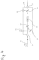
- Fig. 1 is a schematic diagram showing the configuration of the optical demultiplexing module of the present invention.
- the module which is to be placed ahead of an optical fiber 10 doped with a rare earth element such as Er, supplies pumping light into the fiber 10 and passes signal light that is amplified in that fiber.
- a rare earth element such as Er
- a first collimator 1 and a second collimator 5 are provided normal to opposing sides of a square or rectangular housing 8, whereas a third collimator 6 is provided normal to a side of the housing at right angles to the opposing sides.
- Each collimator is formed by providing a lens either at the top end or ahead of the optical fiber and the light passing through the lens either remains parallel or converges at the focus.
- Housing 8 is made of a metal such as SUS or a hard plastic material that are either cut or extrusion molded to form an integral member that has a rugged and stable structure.
- Signal light is admitted into the housing 8 from the first collimator 1 and a multiplexer 2 for transmitting the signal light and reflecting the pumping light is provided on its optical axis.
- An optical isolator 3 for passing the light that travels in the direction indicated by a thick arrow but blocking the light in opposite direction is provided on the optical axis of the light passing through the multiplexer.
- a beam splitter 4 is provided at the output end of the optical isolator for reflecting part of the signal light but transmitting the remainder.
- the multiplexer 2, the optical isolator 3 and the beam splitter 4 are provided in mutual alignment.
- the second collimator 5 is provided on the optical axis of the light passing through the beam splitter 4.
- a reflector mirror 7 is provided on the optical axis of the pumping light to be admitted into the housing 8 from the third collimator 6; the multiplexer 2 is provided on the optical axis of the light to be reflected from the reflector mirror; and the first collimator 1 is provided on the optical axis of the light to be reflected from the multiplexer.
- the multiplexer 2 is so positioned that the angle ⁇ at which the pumping light coming from the third collimator 6 is admitted into the multiplexer is no more than 22.5 degrees.
- a monitoring light-receiving device 9 is provided in the position where part of the signal light as reflected from the beam splitter 4 crosses a side of the housing and this enables monitoring of the signal light level.
- the optical demultiplexing module can be fabricated easily while insuring that the optical devices used are less dependent on polarization and wavelength.
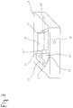
- Fig. 2 is a perspective view of the housing for the optical demultiplexing module shown in Fig. 1.
- the housing indicated by 8 is made of a single member in a square or rectangular form and a first hollow portion 11 and a second hollow portion 12 are formed from the top to the bottom surface in the central area of the housing.
- the first hollow portion 11 has a first inner surface 13 formed for fixing the reflector mirror 7 as it is inclined at a predetermined angle.
- the second hollow portion 12 has a second inner surface 14 and a third inner surface 15 provided for mounting the multiplexer 2 and the beam splitter 4, respectively, as they are inclined at predetermined angles, as well as a space into which the optical isolator 3 is to be inserted and fixed.
- a fourth hole 16 is provided between the first hollow portion 11 and the second hollow portion 12 for passing both the signal light and the pumping light.
- a first hole 17 and a second hole 18 are provided in opposing sides of the housing for mounting the first collimator 1 and the second collimator 5, respectively, normal to the opposing sides, and a third hole 19 is provided in a side of the housing at right angles to the opposing sides for mounting the third collimator 6 normal to the side.
- the first hole 17, the fourth hole 16 and the second hole 18 are provided in such a way that the signal light emitting from the first collimator 1 passes through the multiplexer 2, the optical isolator 3 and the beam splitter 4 to reach the second collimator 5 at a point in alignment with those three elements.
- the first inner surface 13 and the second inner surface 14 are adjusted in the angle ⁇ so that the pumping light emitting from the third collimator 6 is admitted into the first collimator 1 by means of the reflector mirror 7 and the multiplexer 2 which are to be adhesively fixed on the first and second inner surfaces, respectively.
- Fig. 3 is a perspective view showing another housing for the optical demultiplexing module shown in Fig. 1.
- the first hollow portion 11 has a first inner surface 13' and a second inner surface 14' formed for mounting the reflector mirror 7 and the multiplexer 2, respectively, as they are inclined at predetermined angles.
- the second hollow portion 12 has a third inner surface 15 provided for mounting the beam splitter 4 as it is inclined at a predetermined angle, as well as a space into which the optical isolator 3 is to be inserted and fixed.
- a fourth hole 16' is provided between the first hollow portion 11 and the second hollow portion 12 for passing the signal light.
- the first inner surface 13' and the second inner surface 14' are adjusted in the angle ⁇ so that the pumping light emitting from the third collimator is admitted into the first collimator by means of the reflector mirror 7 and the multiplexer 2 which are to be adhesively fixed on the first and second inner surfaces, respectively.
- a hole 20 is provided for mounting an optical monitoring device 9 in the position where part of the signal light as reflected from the beam splitter 4 crosses a side of the housing.
- Fig. 4 is a schematic diagram showing the configuration of an embodiment of the optical multiplexing module of the present invention.
- the module which is to be placed behind a rare-earth element doped optical fiber 10, supplies signal light both and pumping light into the fiber.
- a first collimator 21 and a second collimator 25 are provided normal to opposing sides of a square or rectangular housing 28, whereas a third collimator 26 is provided normal to a side of the housing at right angles to the opposing sides.
- a beam splitter 24 is provided on the optical axis of signal light not yet be amplified which is to be admitted into the housing 28 from the second collimator.
- An optical isolator 23 is provided on the optical axis of the light passing through the beam splitter.
- a multiplexer 22 is provided on the optical axis of the light passing through the optical isolator.
- the first collimator 21 is provided on the optical axis of the light passing through the multiplexer 22.
- a reflector mirror 27 is provided on the optical axis of the excitation to be admitted into the housing 28 from the third collimator 26.
- the multiplexer 22 is provided on the optical axis of the light to be reflected from the reflector mirror.
- the first collimator 21 is provided on the optical axis of the light to be reflected from the multiplexer.
- the multiplexer 22 is so positioned that the angle ⁇ at which the pumping light coming from the third collimator 26 is admitted into the multiplexer is no more than 22.5 degrees.
- a monitoring light-receiving device 29 is provided in the position where part of the signal light as reflected from the beam splitter 24 crosses a side of the housing and this enables monitoring of the signal light level.
- Fig. 5 is a perspective view of the housing for the optical multiplexing module shown in Fig. 4.
- the housing 28 is made of a single member in a square or rectangular form.
- a first hollow portion 11 and a second hollow portion 12 are formed from the top to the bottom surface of the central area of the housing.
- the first hollow portion 11 has a first inner surface 13 formed for fixing the reflector mirror 27 as it is inclined at a predetermined angle.
- the second hollow portion 12 has a second inner surface 14 and a third inner surface IS provided for mounting the multiplexer 22 and the beam splitter 24, respectively, as they are inclined at predetermined angles, as well as a space into which the optical isolator 23 is to be inserted and fixed.
- a fourth hole 16 is provided between the first hollow portion 11 and the second hollow portion 12 for passing both the signal light and the pumping light.
- a first hole 17 and a second hole 2 are provided in opposing sides of the housing for mounting the first collimator 21 and the second collimator 25, respectively, normal to the opposing sides, and a third hole 19 is provided in a side of the housing at right angles to the opposing sides for mounting the third collimator 26 normal to the side.
- the second hole 18, the fourth hole 16 and the first hole 17 are provided in such a way that the signal light emitting from the second collimator 25 passes through the beam splitter 24, the optical isolator 23 and the multiplexer 22 to reach the first collimator 21 at a point in alignment with those three elements.
- the angle 8 is adjusted so that the pumping light emerging from the third collimator 26 is admitted into the first collimator 21 by the reflector mirror 27 and the multiplexer 22 which are to be adhesively fixed on the first and second inner surfaces, respectively.
- a fifth hole 20-1 is provided for mounting a monitoring light-receiving device 29 in the position where part of the split light as reflected from the beam splitter 24 crosses a side of the housing.
- the housing 28 shown in Fig. 5 and the housing 8 shown in Fig. 2 have the same structure except that the fifth hole 20-1 is positioned on the opposite side to the hole 20. Therefore, both of these holes may sometimes be provided in a single housing.
- the housing 28 for an optical multiplexing module in Fig. 6 has the same structure as the housing 8 shown in Fig. 3, except that the fifth hole 20 is replaced by a fifth hole 20-1.
- the housing for accommodating an optical demultiplexing module has essentially the same structure as the housing for accommodating an optical multiplexing module. Therefore, the housing that is adapted for use irrespective of whether the module to be accommodated is for optical demultiplexing or multiplexing purposes will now be described. For the sake of simplicity, the following explanation is directed to the case of an optical demultiplexing module.
- Figs. 7a, 7b and 7c are perspective views showing the structures of the respective parts of the housing of Embodiment 3.
- the housing has a block 31b for supporting the multiplexer 2 and the reflector mirror 7, a block 31c for supporting the optical isolator 3 and the beam splitter 4, and a frame 31a having in the central area a hollow portion 41 into which the blocks 31b and 31c are to be inserted and fixed.
- the frame 31a and blocks 31b and 31c are each made of a metal such as SUS or a hard plastic material that are either cut or extrusion molded to form an integral member that has a rugged and stable structure.
- the frame 31a has the hollow portion 41 formed from the top to the bottom surface in the central area.
- the blocks 31b and 31c are to be inserted and fixed in the hollow portion 41.
- Holes 38a, 38b and 38c are made in sides 40a, 40b and 40c of the frame for fixing the first collimator 1, the second collimator 5 and the third collimator 6, respectively.
- Holes 38j and 38i are made in sides 40c and 40d of the frame so that monitoring light-receiving devices 29 and 9 can be inserted and fixed on those sides normal thereto. Accordingly, since these holes 38j and 38i are provided, the frame is applicable not only to the optical demultiplexing module but also to the optical multiplexing module. Therefore, either one of these holes may be omitted if the other suffices.
- the block 31b is cut obliquely to the side 42b or 42c and to the side 42d or 42a to form recesses 39a and 39b in which the multiplexer 2 and the reflector mirror 7 can be adhesively fixed.
- a cylindrical hole may be bored obliquely through the respective sides to form the same recesses 39a and 39b. The inclination at which the sides of the block 31b are cut or provided with cylindrical holes obliquely is adjusted in such a way that the pumping light emitting from the third collimator 6 is reflected by the reflector mirror 7 and the multiplexer 2 to be admitted into the first collimator 1.
- a hole 38f is provided between the recesses 39a and 39b so that the pumping light as reflected from the reflector mirror 7 reaches the multiplexer 2.
- a hole 38d is provided between the side 42a and the recess 39a for passing both the signal light and the pumping light so that they are admitted or allowed to emit from the first collimator 1 or the third collimator 6.
- a hole 38e is provided between the side 42c and the recess 39b for passing the pumping light so that it is admitted or allowed to emit from the first collimator or the third collimator.
- the block 31c is cut obliquely to the side 43b or 43d to form a recess 39c in which the beam splitter 4 can be adhesively fixed.
- a cylindrical hole may be bored obliquely through the respective side to form the same recess 39c.
- a hole 44 is provided in the side 43a for passing the signal light from the optical isolator 3 toward the beam splitter 4. Also, the hole 44 passes the signal light not yet be amplified which is to be admitted into the optical isolator from the second collimator 25.
- a hole 38g is provided connecting the bottom of the hole 44 to the recess 39c.
- a hole 38h for insuring that part of the signal light passing through the optical isolator 3 is reflected by the beam splitter 4 to reach the monitoring light-receiving device 29.
- the hole 38h also passes part of the signal light passing through the second collimator as reflected from the beam splitter 24.
- Fig. 8 is a perspective view showing the combination of frame 31a, block 31b and block 31c after the necessary optical devices are installed and adjusted in relative positions, followed by fixing the blocks in the frame to form an integral assembly by YAG laser welding or some other suitable method.
- holes 38d, 38e, 38f, 38g and 38h are provided simply for the purpose of passing the signal light and, hence, may be replaced by generally U-shaped grooves.
- both the optical demultiplexing and multiplying modules of the present invention are so adapted that pumping light is admitted into the multiplexer at incident angles of no more than 22.5 degrees and, hence, their dependency on polarization and wavelength can be held at consistently low levels.
- signal light is not reflected within the housing but travels straight to be launched into or pass through the amplifying fiber, hence experiences small insertion loss.
- each of the collimators is mounted normal to the associated side of the housing and, hence, optical devices can be assembled and adjusted in the housing by simple procedures.
- the invention also provides a housing for an optical demultiplexing/multiplexing module having one frame and two blocks. Individual devices are assembled and adjusted in each separate block and the blocks thus accommodating the necessary devices are combined together within the frame to complete the dual module. Hence, small optical devices can be easily assembled and adjusted within a limited space.
Landscapes
- Physics & Mathematics (AREA)
- Electromagnetism (AREA)
- Engineering & Computer Science (AREA)
- Optics & Photonics (AREA)
- Plasma & Fusion (AREA)
- General Physics & Mathematics (AREA)
- Computer Networks & Wireless Communication (AREA)
- Microelectronics & Electronic Packaging (AREA)
- Signal Processing (AREA)
- Optical Couplings Of Light Guides (AREA)
- Optical Communication System (AREA)
- Lasers (AREA)
- Light Receiving Elements (AREA)
Applications Claiming Priority (4)
| Application Number | Priority Date | Filing Date | Title |
|---|---|---|---|
| JP274485/93 | 1993-11-02 | ||
| JP27448593 | 1993-11-02 | ||
| JP139984/94 | 1994-06-22 | ||
| JP6139984A JPH07174933A (ja) | 1993-11-02 | 1994-06-22 | 光分岐・合波モジュール及び筐体 |
Publications (2)
| Publication Number | Publication Date |
|---|---|
| EP0651475A2 true EP0651475A2 (de) | 1995-05-03 |
| EP0651475A3 EP0651475A3 (de) | 1995-11-29 |
Family
ID=26472632
Family Applications (1)
| Application Number | Title | Priority Date | Filing Date |
|---|---|---|---|
| EP94117290A Withdrawn EP0651475A3 (de) | 1993-11-02 | 1994-11-02 | Optischer Demultiplexier/Multiplexiermodul und ein Gehäuse dafür. |
Country Status (5)
| Country | Link |
|---|---|
| US (1) | US5510932A (de) |
| EP (1) | EP0651475A3 (de) |
| JP (1) | JPH07174933A (de) |
| KR (1) | KR950016057A (de) |
| AU (1) | AU7761394A (de) |
Cited By (5)
| Publication number | Priority date | Publication date | Assignee | Title |
|---|---|---|---|---|
| EP0723170A3 (de) * | 1995-01-19 | 1997-04-23 | Sumitomo Electric Industries | Optisches zusammengesetztes Modul und Verfahren zu dessen Aufbau |
| WO1998021787A1 (de) * | 1996-11-08 | 1998-05-22 | Daimlerchrysler Ag | Diodengepumpter, frequenzverdoppelter festkörperlaser |
| WO2003012510A1 (en) * | 2001-07-27 | 2003-02-13 | Gigabit Optics Corporation | System and method for optical multiplexing and/or demultiplexing |
| WO2004054051A1 (ja) * | 2002-12-06 | 2004-06-24 | Central Glass Company, Limited | 光ファイバ増幅器モジュール |
| EP2088464A4 (de) * | 2006-12-31 | 2009-11-04 | Huawei Tech Co Ltd | Faserverstärker, herstellungsverfahren dafür und faserkommunikationssystem |
Families Citing this family (8)
| Publication number | Priority date | Publication date | Assignee | Title |
|---|---|---|---|---|
| JP3062060B2 (ja) * | 1995-09-13 | 2000-07-10 | 日本電気株式会社 | 光電気変換回路 |
| JP3778641B2 (ja) * | 1996-12-13 | 2006-05-24 | 富士通株式会社 | 光増幅器 |
| JP3495578B2 (ja) * | 1997-10-03 | 2004-02-09 | 古河電気工業株式会社 | 光ファイバ増幅器 |
| JP3650591B2 (ja) * | 2000-08-21 | 2005-05-18 | 古河電気工業株式会社 | 光結合モジュールの光軸修正方法 |
| US20040022494A1 (en) * | 2002-08-05 | 2004-02-05 | Liddle James A. | Fiber optic array with fiber tap and methd for making and using |
| US6932520B2 (en) * | 2003-02-03 | 2005-08-23 | Jds Uniphase Corporation | Modular optical components |
| WO2008035430A1 (fr) * | 2006-09-21 | 2008-03-27 | Hoya Corporation | Module optique |
| US20230121874A1 (en) * | 2021-10-19 | 2023-04-20 | Mellanox Technologies, Ltd. | Integrated Optical Switch Having Doped Fiber/Waveguide Amplifiers Packaged in A Transposer |
Family Cites Families (14)
| Publication number | Priority date | Publication date | Assignee | Title |
|---|---|---|---|---|
| FR2516254B1 (fr) * | 1981-11-12 | 1985-09-13 | Comp Generale Electricite | Separateur optique pour la separation ou la superposition de deux faisceaux de lumiere |
| US4701010A (en) * | 1984-08-30 | 1987-10-20 | Adc Fiber Optics Corporation | Unitary body optical coupler |
| US4767171A (en) * | 1986-03-27 | 1988-08-30 | Siemens Aktiengesellschaft | Transmission and reception module for a bidirectional communication network |
| DE3801764A1 (de) * | 1988-01-22 | 1989-08-03 | Ant Nachrichtentech | Wellenlaengenmultiplexer oder -demultiplexer, sowie verfahren zur herstellung des wellenlaengenmultiplexers oder -demultiplexers |
| JPH01292875A (ja) * | 1988-05-20 | 1989-11-27 | Oki Electric Ind Co Ltd | 半導体光増幅モジュール |
| JP2786725B2 (ja) * | 1989-07-20 | 1998-08-13 | 住友電気工業株式会社 | 光ファイバおよびファイバ光能動装置 |
| CA2037350C (en) * | 1990-03-02 | 1994-11-08 | Kenichi Abe | Optical coupler |
| JP2649737B2 (ja) * | 1990-07-05 | 1997-09-03 | 国際電信電話株式会社 | 光増幅器の励起光源駆動方式 |
| US5140466A (en) * | 1990-12-20 | 1992-08-18 | Hughes Aircraft Company | Optical multiplexer |
| US5191467A (en) * | 1991-07-24 | 1993-03-02 | Kaptron, Inc. | Fiber optic isolater and amplifier |
| US5299056A (en) * | 1992-05-06 | 1994-03-29 | Matsushita Electric Industrial Co., Ltd. | Optical passive component assembly |
| JPH05341233A (ja) * | 1992-06-10 | 1993-12-24 | Fujitsu Ltd | 光増幅器用光モジュール |
| JP3251330B2 (ja) * | 1992-06-10 | 2002-01-28 | 富士通株式会社 | 光増幅器用光モジュール |
| JP3453767B2 (ja) * | 1992-06-10 | 2003-10-06 | 富士通株式会社 | 光増幅器用光モジュール |
-
1994
- 1994-06-22 JP JP6139984A patent/JPH07174933A/ja active Pending
- 1994-11-01 AU AU77613/94A patent/AU7761394A/en not_active Abandoned
- 1994-11-01 KR KR1019940028463A patent/KR950016057A/ko not_active Withdrawn
- 1994-11-02 EP EP94117290A patent/EP0651475A3/de not_active Withdrawn
- 1994-11-02 US US08/333,344 patent/US5510932A/en not_active Expired - Fee Related
Cited By (13)
| Publication number | Priority date | Publication date | Assignee | Title |
|---|---|---|---|---|
| EP0723170A3 (de) * | 1995-01-19 | 1997-04-23 | Sumitomo Electric Industries | Optisches zusammengesetztes Modul und Verfahren zu dessen Aufbau |
| WO1998021787A1 (de) * | 1996-11-08 | 1998-05-22 | Daimlerchrysler Ag | Diodengepumpter, frequenzverdoppelter festkörperlaser |
| US6282227B1 (en) | 1996-11-08 | 2001-08-28 | Eads Deutschland Gmbh | Diode-pumped double frequency solid-state laser |
| US6781693B2 (en) | 2001-07-27 | 2004-08-24 | Gigabit Optics Corporation | System and method for optical multiplexing and/or demultiplexing |
| US6750969B2 (en) | 2001-07-27 | 2004-06-15 | Gigabit Optics Corporation | System and method for optical multiplexing and/or demultiplexing |
| WO2003012510A1 (en) * | 2001-07-27 | 2003-02-13 | Gigabit Optics Corporation | System and method for optical multiplexing and/or demultiplexing |
| US6844932B2 (en) | 2001-07-27 | 2005-01-18 | Oplink Communications, Inc. | System and method for optical multiplexing and/or demultiplexing |
| US6847450B2 (en) | 2001-07-27 | 2005-01-25 | Oplink Communications, Inc. | System and method for optical multiplexing and/or demultiplexing |
| US6856435B2 (en) | 2001-07-27 | 2005-02-15 | Gigabit Optics Corporation | System and method for optical multiplexing and/or demultiplexing |
| US6914676B2 (en) | 2001-07-27 | 2005-07-05 | Oplink Communications, Inc. | System and method for optical multiplexing and/or demultiplexing |
| WO2004054051A1 (ja) * | 2002-12-06 | 2004-06-24 | Central Glass Company, Limited | 光ファイバ増幅器モジュール |
| EP2088464A4 (de) * | 2006-12-31 | 2009-11-04 | Huawei Tech Co Ltd | Faserverstärker, herstellungsverfahren dafür und faserkommunikationssystem |
| US8098425B2 (en) | 2006-12-31 | 2012-01-17 | Huawei Technologies Co., Ltd. | Fiber communication system, fiber amplifier, and method for fabricating fiber amplifier |
Also Published As
| Publication number | Publication date |
|---|---|
| AU7761394A (en) | 1995-05-18 |
| KR950016057A (ko) | 1995-06-17 |
| US5510932A (en) | 1996-04-23 |
| EP0651475A3 (de) | 1995-11-29 |
| JPH07174933A (ja) | 1995-07-14 |
Similar Documents
| Publication | Publication Date | Title |
|---|---|---|
| US6493121B1 (en) | Bidirectional module for multichannel use | |
| US5661835A (en) | Optical composite module and method of assembling the same | |
| US5917648A (en) | Packaged optical amplifier assembly | |
| US5510932A (en) | Optical demultiplexing module, optical multiplexing module and housings therefor | |
| US7198416B2 (en) | Optical combiner device | |
| US5299056A (en) | Optical passive component assembly | |
| US6922281B2 (en) | Erbium-doped fiber amplifier and integrated module components | |
| JP4639578B2 (ja) | 半導体レーザモジュール及びその製造方法 | |
| US6081635A (en) | Microoptical module with a WDM filter and an optical isolator for fiber-optic amplifier systems | |
| US6381066B1 (en) | Integrated semiconductor optical amplifier system | |
| US6513991B1 (en) | Semiconductor optical device package | |
| US7043101B1 (en) | Integrated optical pump module | |
| JP3453767B2 (ja) | 光増幅器用光モジュール | |
| JPH06181352A (ja) | 光増幅器用光モジュール | |
| JPH0888430A (ja) | 光ファイバ増幅器 | |
| WO1996012986A1 (en) | Optical devices including optical isolators | |
| JPH11295564A (ja) | 光アイソレータモジュールと光アイソレータ部品 | |
| JPH0764021A (ja) | 光結合器及び光ファイバ増幅器 | |
| JPH1079702A (ja) | 光通信用モジュール | |
| JPS63225206A (ja) | ハイブリツド合分波器 | |
| JPH1126875A (ja) | 光複合モジュール | |
| KR100248051B1 (ko) | 정렬간극 관측용 슬릿홈을 구비한 광아이솔레이터 | |
| JPH07301763A (ja) | 光結合器及び光ファイバ増幅器 | |
| JPH07335956A (ja) | 光増幅器及び受光装置 | |
| JP3833280B2 (ja) | 光学部品 |
Legal Events
| Date | Code | Title | Description |
|---|---|---|---|
| PUAI | Public reference made under article 153(3) epc to a published international application that has entered the european phase |
Free format text: ORIGINAL CODE: 0009012 |
|
| AK | Designated contracting states |
Kind code of ref document: A2 Designated state(s): DE FR GB IT SE |
|
| PUAL | Search report despatched |
Free format text: ORIGINAL CODE: 0009013 |
|
| AK | Designated contracting states |
Kind code of ref document: A3 Designated state(s): DE FR GB IT SE |
|
| STAA | Information on the status of an ep patent application or granted ep patent |
Free format text: STATUS: THE APPLICATION IS DEEMED TO BE WITHDRAWN |
|
| 18D | Application deemed to be withdrawn |
Effective date: 19960530 |