EP0652522A1 - Steuerungsschaltkreis für Datenausgabe-Auffang-Flipflop und Verfahren für Halbleiterspeichersystem - Google Patents
Steuerungsschaltkreis für Datenausgabe-Auffang-Flipflop und Verfahren für Halbleiterspeichersystem Download PDFInfo
- Publication number
- EP0652522A1 EP0652522A1 EP94116321A EP94116321A EP0652522A1 EP 0652522 A1 EP0652522 A1 EP 0652522A1 EP 94116321 A EP94116321 A EP 94116321A EP 94116321 A EP94116321 A EP 94116321A EP 0652522 A1 EP0652522 A1 EP 0652522A1
- Authority
- EP
- European Patent Office
- Prior art keywords
- signal
- data bus
- valid data
- latch
- control circuit
- Prior art date
- Legal status (The legal status is an assumption and is not a legal conclusion. Google has not performed a legal analysis and makes no representation as to the accuracy of the status listed.)
- Withdrawn
Links
- 238000000034 method Methods 0.000 title claims abstract description 17
- 239000004065 semiconductor Substances 0.000 title claims description 14
- 230000008569 process Effects 0.000 title abstract description 11
- 238000011161 development Methods 0.000 claims abstract description 21
- 230000004044 response Effects 0.000 claims abstract description 20
- 238000012544 monitoring process Methods 0.000 claims abstract description 10
- 230000011664 signaling Effects 0.000 claims description 10
- 238000001514 detection method Methods 0.000 claims 1
- 230000007704 transition Effects 0.000 claims 1
- 238000012545 processing Methods 0.000 abstract description 4
- 210000004027 cell Anatomy 0.000 description 9
- 238000010586 diagram Methods 0.000 description 8
- 210000000352 storage cell Anatomy 0.000 description 5
- 238000013459 approach Methods 0.000 description 4
- 238000011068 loading method Methods 0.000 description 4
- 238000013500 data storage Methods 0.000 description 3
- 238000012546 transfer Methods 0.000 description 3
- 230000003139 buffering effect Effects 0.000 description 2
- 230000005669 field effect Effects 0.000 description 2
- 230000000977 initiatory effect Effects 0.000 description 2
- 230000005055 memory storage Effects 0.000 description 2
- 238000012986 modification Methods 0.000 description 2
- 230000004048 modification Effects 0.000 description 2
- 238000004513 sizing Methods 0.000 description 2
- 230000008859 change Effects 0.000 description 1
- 230000003111 delayed effect Effects 0.000 description 1
- 230000000694 effects Effects 0.000 description 1
- 230000008030 elimination Effects 0.000 description 1
- 238000003379 elimination reaction Methods 0.000 description 1
- 238000005516 engineering process Methods 0.000 description 1
- 230000008707 rearrangement Effects 0.000 description 1
- 230000000630 rising effect Effects 0.000 description 1
- 238000006467 substitution reaction Methods 0.000 description 1
Images


Classifications
-
- G—PHYSICS
- G11—INFORMATION STORAGE
- G11C—STATIC STORES
- G11C7/00—Arrangements for writing information into, or reading information out from, a digital store
- G11C7/22—Read-write [R-W] timing or clocking circuits; Read-write [R-W] control signal generators or management
Definitions
- the present invention relates generally to semiconductor memory systems, and more particularly, to a control circuit and control process for a read access wherein a read command is timed to enable data output latches substantially simultaneous with development of valid data on the memory system data bus.
- Today's semiconductor memory systems employ multiple subarrays of memory storage units closely packed together. Each subarray is segmented into multiple rows or words, with each word containing multiple data storage cells. Each data storage cell accommodates a bit of data. Typically these multiple subarrays of memory storage units are coupled together by numerous common interconnections, including a common system data bus.
- a system control circuit oversees selection of a particular data storage cell and transfer of that cell's data to the common system data bus for output from the memory system.
- RC read command
- the read command (RC) is generated by the control circuit in response to an externally-generated read clock signal. Without added delay, the read command (RC) is generated long before data on the system data bus becomes valid. Since the system data bus is common to all subarrays, it has significant associated capacitance which in the case of a low state signal must be dissipated before the data signal can become valid. In such a case, the cross-coupled connections of the data output latches are unnecessarily exposed to the stored charge on the system data bus (rather than a valid low state signal) and possibly unnecessarily switched to the wrong data value.
- RC read command
- the invention comprises in one aspect a control circuit for a memory system having a common system data bus coupled to at least one data output latch.
- the control circuit generates a read command to enable the at least one data output latch to latch data from the system data bus in response to a read clock signal.
- the control circuit includes detecting means for detecting the read clock signal and for generating in response thereto a latch enable signal.
- Signaling means independent of the system data bus provides a valid data signal representative of valid data occurring on the system data bus.
- The, valid data signal is generated by the signaling means without direct monitoring of the system data bus.
- a control means is coupled to the detecting means and the signaling means for providing the read command to the at least one data output latch upon occurrence of both the latch enable signal and the valid data signal.
- the invention comprises a control circuit for a memory system having multiple memory subarrays and a common system data bus coupled to at least one data output latch.
- the control circuit generates a read command to enable the at least one data output latch to latch valid data from the system data bus in response to a read clock signal.
- the control circuit includes a detecting means for detecting the read clock signal and for generating in response thereto a latch enable signal.
- a dummy circuit is associated with each memory subarray for generating in response to the read clock signal, independent of the system data bus, a valid data signal representative of valid data occurring on the system data bus.
- Control means is coupled to the detecting means and to the dummy circuit for providing the read command to the at least one data output latch upon occurrence of both the latch enable signal and the valid data signal.
- the present invention comprises a method for generating a read command within a memory system having a common system data bus coupled to at least one data output latch.
- the read command enables the at least one data output latch to latch valid data from the system data bus in response to a read clock signal.
- the method includes the steps of: detecting the read clock signal and generating in response thereto a latch enable signal; generating without monitoring the system data bus a valid data signal representative of valid data occurring on the system data bus; and providing the read command to the at least one data output latch upon occurrence of both the latch enable signal and the valid data signal.
- this invention comprises a novel control circuit and process approach for overseeing a read access cycle within a semiconductor memory system.
- the approach is to precisely generate a read command substantially simultaneous with development of valid data on the system data bus.
- the read access cycle can be shortened, thereby improving system performance.
- the concepts presented apply to any memory system including RAMs, ROMs, DRAMs, SRAMs, etc. Reduced system noise and power losses result from ensuring elimination of double switching at the data output latches.
- the control circuit and control process are independent of the system data bus, requiring no direct monitoring of the common bus.
- System 10 which is to incorporate a control circuit and control processing in accordance with the present invention, includes a control circuit 12 coupled to multiple memory subarrays 14 each of which receives and transfers data through a common system data bus 16.
- Addressing and control circuit 12 includes an addressing system 18, a subarray column select 20, a row select 22 and a column I/O 24. These circuits are each well known to those skilled in the art and are well documented in the available literature.
- Inputs to circuit 12 include an "Address Signal”, a “Data In” signal (during a write cycle), and “read clock” and “write clock” signals which initiate read cycles and write cycles, respectively.
- Output from circuit 12 is a parallel "Data Out” signal, provided via a plurality of data output latches 26. Each valid data bit is transferred from the system data bus to a corresponding data output latch of latches 26.
- system data bus 16 comprises 36 bits
- control circuit 12 includes 36 data output latches 26. These latches are typically disposed within column I/O block 24 of control circuit 12.
- each data output latch 26' (Fig. 2) is clocked by a read command (RC) produced by control circuit 12 of memory system 10 in response to the read clock signal (RCLK).
- RC read clock signal
- each data output latch 26' sets based upon the present data value of the corresponding bit of system data bus 16.
- the "Data Out" signal from control circuit 12 is taken in parallel from the multiple data output latches 26.
- the timing diagram of Fig. 3 illustrates the problem inherent in a conventional read access.
- a read clock signal RCLK
- the control circuit Upon receipt of a read clock signal (RCLK) the control circuit generates a read command (RC), which is identical to but delayed slightly from the read clock signal (RCLK). The delay results from circuit buffering and capacitance.
- the read command (RC) is the enabling signal which clocks the data output latches coupled to the system data bus.
- V dd high state
- the data output latch has undergone a double switching, which unnecessarily increases noise and power dissipation within the semiconductor memory system.
- the problem exists in this example only when the valid data value is other than the precharge value applied to the system data bus during the precharge cycle.
- the existing solution to the problem has been to delay the enabling read command (RC) until a time that the system designer can guarantee valid data exists on the system data bus.
- RC enabling read command
- a control circuit (and control process) in accordance with the present invention precisely controls the generation of the read command (RC) in response to positive information so that the read command (RC) occurs simultaneous with or, if preferred, at a time interval slightly prior to, the instant that valid data develops on the system data bus.
- Fig. 4 comprises one timing diagram example for such a control circuit and process.
- the read command (RC) no longer automatically follows the read clock (RCLK) by a small delay but rather (pursuant to the invention) is tied to the instant at which valid data develops on the system data bus.
- the read command (RC) is generated at a small predefined time interval 't' prior to the instant 'x' valid data develops on the system data bus. (Attainment of offset 't' is discussed below.) Thus, assuming that the data output latch must switch, only a single switching of the latch occurs.
- the present control process includes detecting the read clock signal (RCLK) and generating in response thereto a latch enable signal; providing positive information on when a valid data signal occurs on the system data bus and generating the read command (RC) for the data output latches only upon occurrence of both the latch enable signal and the valid data signal.
- RCLK read clock signal
- the valid data signal is efficiently generated independent of the system data bus, i.e., there is no direct monitoring of the system data bus to determine when valid data occurs.
- a dummy circuit including a duly bus is provided to develop a data valid signal that switches state simultaneous with development of valid data on the system data bus, or at a precise, predefined time interval prior to development of valid data on the system data bus.
- Fig. 5 partially depicts one embodiment of a memory subarray employing this concept.
- Each word 29 of subarray 14 includes a dummy cell 30 which, for example, is constructed to transfer (over a dummy bitline 33) a low state to a dummy bus 31 whenever the corresponding word is read.
- the dummy circuit includes dummy cells 30, dummy bitlines 33 and the common dummy bus 31. Note that reading of a word within one of the subarrays of the memory system triggers the dummy circuit (through the corresponding dummy cell) to generate the valid data signal.
- Simultaneous switching can be attained by appropriately sizing the dummy bus and connecting the bus to receive the same capacitive loading as the system data bus.
- the dummy data bus is driven by the same number of read heads as that driving the system data bus.
- dummy bus switching can precede the instant of valid data development on the system data bus by a predefined time interval.
- Early triggering of the dummy bus can be attained by reducing loading on dummy bus 31, or reducing loading on dummy bitline 33. This is necessarily a trial and error exercise to be performed by the system designer.
- the goal is to have the valid data signal (i.e., switching signal DBUS) of the dummy data bus precede the instant of valid data signal development on the system data bus by a small, desired interval of time 't' to ensure that the latches are enabled at the instant of valid data development.
- the same result could also be obtained by one of ordinary skill in the art by modifying the size of the dummy cells associated with the words of the subarrays relative to the size of the storage cells.
- the dummy bus 31 undergoes the same precharge cycle as system data bus 16 so that dummy bus 31 begins every read cycle with a high state and switches to a low state with the low signal output from the corresponding dummy cell 30 of the read word within a subarray.
- One skilled in the art can readily fabricate the dummy cells 30 to consistently output a low state signal whenever the associated word is read; for example, by tying each dummy cell's cross-couple node to ground.
- a low state signal on dummy bus 31 comprises the "data valid signal.” Note that this signal coincides with and "represents" development of valid data on the system data bus since the dummy circuit components have the same sizings and experience the same loadings as the system's storage cells, bitlines, and common data bus. Further, the signal is arrived at independent of any direct monitoring of the system data bus.
- the data valid signal is employed by a control circuit in accordance with the present invention to generate the read command (RC).
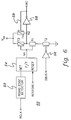
- Fig. 6 depicts one embodiment of a control circuit 50 for generating the read command (RC) pursuant to the present invention.
- Control circuit 50 includes a rising edge detector 52 coupled to receive the read clock signal (RCLK). Detector 52 outputs a "set” pulse to the set input of a flip flop latch 54 whenever the read clock signal (RCLK) goes active.
- Latch 54 provides a high signal at its output node N1 when set. The signal at node N1, referred to herein as a "latch enable signal," gates an NFET T1 and a PFET T3 connected as shown.
- P-channel field-effect transistors are indicated by a rectangle with a diagonal line formed therein and a control element or gate electrode arranged adjacent thereto and N-channel field-effect transistors (NFETs) are indicated by a rectangle without a diagonal line and with a control element or gate electrode arranged adjacent thereto.
- PFETs P-channel field-effect transistors
- NFETs N-channel field-effect transistors
- a high signal at node N1 turns PFET T3 "off” and NFET T1 "on". NFET T1 is non-conducting, however, until a serially connected NFET T2 is also activated.
- the dummy bus (DBUS) is assumed to be precharged high (from the precharge cycle) and is switched low by the appropriate dummy cell as an indication that valid data exists (or is about to exist) on the system data bus. This signal is referred to herein as the "valid data signal”.
- a high state signal on the dummy bus is inverted by an inverter circuit 56 to provide a low state signal to NFET T2 during the precharge cycle and prior to development of valid data on the system data bus.
- inverter circuit 56 Upon switching to a low state, inverter circuit 56 provides a high control signal at the gate of NFET T2, thereby turning the transistor "on” and allowing current to flow to ground. This forces a low signal at node N2 of circuit 50, which in turn is inverted by an inverter circuit 58 to a high, enabling read command (RC) output.
- a high read command (RC) is interpreted within the present example as an indication that valid data now exists on the system data bus.
- feedback 59 can be provided from the output node of control circuit 50 to the gate of a PFET T4 to assist in driving the circuit output node low when the read command (RC) is discontinued.
- this invention presents a novel control circuit and control process for a read access cycle within a semiconductor memory system.
- the control approach precisely generates a read command (RC) substantially simultaneous with development of valid data on the system data bus.
- RC read command
- the read access cycle is shortened, thereby improving system performance.
- the concepts presented apply to any memory system including RAMs, ROMs, DRAMs, SRAMs, etc. Reduced noise and power losses result from eliminating double switching at the data output latches.
- the control circuit and control process are independent of the system data bus, with no direct monitoring and feedback from the system data bus required.
Landscapes
- Dram (AREA)
- Memory System (AREA)
- Semiconductor Memories (AREA)
- Static Random-Access Memory (AREA)
Applications Claiming Priority (2)
| Application Number | Priority Date | Filing Date | Title |
|---|---|---|---|
| US148601 | 1993-11-08 | ||
| US08/148,601 US5383155A (en) | 1993-11-08 | 1993-11-08 | Data output latch control circuit and process for semiconductor memory system |
Publications (1)
| Publication Number | Publication Date |
|---|---|
| EP0652522A1 true EP0652522A1 (de) | 1995-05-10 |
Family
ID=22526494
Family Applications (1)
| Application Number | Title | Priority Date | Filing Date |
|---|---|---|---|
| EP94116321A Withdrawn EP0652522A1 (de) | 1993-11-08 | 1994-10-17 | Steuerungsschaltkreis für Datenausgabe-Auffang-Flipflop und Verfahren für Halbleiterspeichersystem |
Country Status (3)
| Country | Link |
|---|---|
| US (1) | US5383155A (de) |
| EP (1) | EP0652522A1 (de) |
| JP (1) | JP3072698B2 (de) |
Families Citing this family (13)
| Publication number | Priority date | Publication date | Assignee | Title |
|---|---|---|---|---|
| JPH07211077A (ja) * | 1993-12-03 | 1995-08-11 | Toshiba Micro Electron Kk | 半導体記憶装置 |
| JPH09288888A (ja) * | 1996-04-22 | 1997-11-04 | Mitsubishi Electric Corp | 半導体記憶装置 |
| US5852373A (en) * | 1996-09-30 | 1998-12-22 | International Business Machines Corporation | Static-dynamic logic circuit |
| US5875152A (en) * | 1996-11-15 | 1999-02-23 | Macronix International Co., Ltd. | Address transition detection circuit for a semiconductor memory capable of detecting narrowly spaced address changes |
| AU5800698A (en) * | 1996-12-27 | 1998-07-31 | Intel Corporation | Single-phase domino time borrowing logic with clocks at first and last stages and latch at last stage |
| US6044024A (en) * | 1998-01-14 | 2000-03-28 | International Business Machines Corporation | Interactive method for self-adjusted access on embedded DRAM memory macros |
| US6154045A (en) * | 1998-12-22 | 2000-11-28 | Intel Corporation | Method and apparatus for reducing signal transmission delay using skewed gates |
| JP3924107B2 (ja) * | 2000-03-09 | 2007-06-06 | 富士通株式会社 | 半導体集積回路 |
| AU2003281787A1 (en) * | 2002-07-31 | 2004-02-23 | Koninklijke Philips Electronics N.V. | Data processing circuit |
| US7184328B2 (en) | 2004-10-18 | 2007-02-27 | Infineon Technologies Ag | DQS for data from a memory array |
| US20070026266A1 (en) * | 2005-07-19 | 2007-02-01 | Pelton Walter E | Distributed electrochemical cells integrated with microelectronic structures |
| KR100897280B1 (ko) * | 2007-09-04 | 2009-05-14 | 주식회사 하이닉스반도체 | 리시버 회로 |
| US7701782B2 (en) * | 2007-09-13 | 2010-04-20 | Micron Technology, Inc. | Signal transfer apparatus and methods |
Citations (3)
| Publication number | Priority date | Publication date | Assignee | Title |
|---|---|---|---|---|
| WO1984001230A1 (en) * | 1982-09-23 | 1984-03-29 | Motorola Inc | Serial data mode circuit for a memory |
| EP0452649A2 (de) * | 1990-04-16 | 1991-10-23 | International Business Machines Corporation | Verriegeltes On-Chip-Fehlererkennungs- und -korrektursystem |
| EP0607670A1 (de) * | 1993-01-21 | 1994-07-27 | Advanced Micro Devices, Inc. | Datenverrieglung |
Family Cites Families (10)
| Publication number | Priority date | Publication date | Assignee | Title |
|---|---|---|---|---|
| JPS59151396A (ja) * | 1983-02-15 | 1984-08-29 | Sharp Corp | 半導体読み出し専用メモリ回路 |
| JPH0799627B2 (ja) * | 1987-01-23 | 1995-10-25 | 松下電器産業株式会社 | 半導体メモリの書き込み読み出し回路 |
| KR970008786B1 (ko) * | 1987-11-02 | 1997-05-29 | 가부시기가이샤 히다찌세이사꾸쇼 | 반도체 집적회로 |
| US4954992A (en) * | 1987-12-24 | 1990-09-04 | Mitsubishi Denki Kabushiki Kaisha | Random access memory having separate read out and write in bus lines for reduced access time and operating method therefor |
| US4864574A (en) * | 1988-02-04 | 1989-09-05 | Rockwell International Corporation | Injection lock clock detection apparatus |
| US4953130A (en) * | 1988-06-27 | 1990-08-28 | Texas Instruments, Incorporated | Memory circuit with extended valid data output time |
| US5031150A (en) * | 1988-08-26 | 1991-07-09 | Kabushiki Kaisha Toshiba | Control circuit for a semiconductor memory device and semiconductor memory system |
| US4975877A (en) * | 1988-10-20 | 1990-12-04 | Logic Devices Incorporated | Static semiconductor memory with improved write recovery and column address circuitry |
| US5077690A (en) * | 1989-08-09 | 1991-12-31 | Atmel Corporation | Memory input data test arrangement |
| JPH04212774A (ja) * | 1990-07-02 | 1992-08-04 | Mitsubishi Electric Corp | 半導体記憶装置 |
-
1993
- 1993-11-08 US US08/148,601 patent/US5383155A/en not_active Expired - Fee Related
-
1994
- 1994-10-17 EP EP94116321A patent/EP0652522A1/de not_active Withdrawn
- 1994-10-19 JP JP6253640A patent/JP3072698B2/ja not_active Expired - Lifetime
Patent Citations (3)
| Publication number | Priority date | Publication date | Assignee | Title |
|---|---|---|---|---|
| WO1984001230A1 (en) * | 1982-09-23 | 1984-03-29 | Motorola Inc | Serial data mode circuit for a memory |
| EP0452649A2 (de) * | 1990-04-16 | 1991-10-23 | International Business Machines Corporation | Verriegeltes On-Chip-Fehlererkennungs- und -korrektursystem |
| EP0607670A1 (de) * | 1993-01-21 | 1994-07-27 | Advanced Micro Devices, Inc. | Datenverrieglung |
Also Published As
| Publication number | Publication date |
|---|---|
| US5383155A (en) | 1995-01-17 |
| JPH07201179A (ja) | 1995-08-04 |
| JP3072698B2 (ja) | 2000-07-31 |
Similar Documents
| Publication | Publication Date | Title |
|---|---|---|
| US5455802A (en) | Dual dynamic sense amplifiers for a memory array | |
| US5325337A (en) | Random access memories (RAM) and more particularly to self-timed RAMS | |
| EP0347530B1 (de) | Statische RAM-Speicheranordnung mit einer Leistungsverminderungsfunktion | |
| US4928266A (en) | Static ram with high speed, low power reset | |
| US20020054535A1 (en) | Random access memory having a read/write address bus and process for writing to and reading from the same | |
| EP0107415B1 (de) | Statische Speicherschaltung | |
| JPS59178685A (ja) | 半導体記憶回路 | |
| US5383155A (en) | Data output latch control circuit and process for semiconductor memory system | |
| JPH0650599B2 (ja) | 半導体メモリ | |
| US5491663A (en) | Pre-charged slave latch with parallel previous state memory | |
| US6741512B2 (en) | Integrated circuit memory devices having efficient multi-row address test capability and methods of operating same | |
| EP0646926B1 (de) | Schaltung zum Abschalten eines Flankendetektors zum Ändern der Betriebscharakteristiken eines Speichers | |
| US5640365A (en) | Semiconductor memory device with a decoding peripheral circuit for improving the operation frequency | |
| JP3800463B2 (ja) | 同期型半導体メモリ装置 | |
| US4800531A (en) | Address buffer circuit for a dram | |
| KR0157289B1 (ko) | 컬럼 선택 신호 제어회로 | |
| EP1278198B1 (de) | Halbleiterspeicheranordnung | |
| US4823322A (en) | Dynamic random access memory device having an improved timing arrangement | |
| JP2003030991A (ja) | メモリ | |
| US5796271A (en) | Memory array having redundant word line | |
| KR0164797B1 (ko) | 라이트 리커버리 제어회로 및 그 제어방법 | |
| US4841279A (en) | CMOS RAM data compare circuit | |
| JPH01116992A (ja) | センス増幅器制御回路 | |
| JP2572607B2 (ja) | 半導体記憶装置 | |
| US20050128845A1 (en) | Device and method for decoding an address word into word-line signals |
Legal Events
| Date | Code | Title | Description |
|---|---|---|---|
| PUAI | Public reference made under article 153(3) epc to a published international application that has entered the european phase |
Free format text: ORIGINAL CODE: 0009012 |
|
| AK | Designated contracting states |
Kind code of ref document: A1 Designated state(s): DE FR GB |
|
| 17P | Request for examination filed |
Effective date: 19950907 |
|
| STAA | Information on the status of an ep patent application or granted ep patent |
Free format text: STATUS: THE APPLICATION HAS BEEN WITHDRAWN |
|
| 18W | Application withdrawn |
Withdrawal date: 19961029 |