EP0653789A2 - Structure de boîtier électronique et sa fabrication - Google Patents
Structure de boîtier électronique et sa fabrication Download PDFInfo
- Publication number
- EP0653789A2 EP0653789A2 EP94115979A EP94115979A EP0653789A2 EP 0653789 A2 EP0653789 A2 EP 0653789A2 EP 94115979 A EP94115979 A EP 94115979A EP 94115979 A EP94115979 A EP 94115979A EP 0653789 A2 EP0653789 A2 EP 0653789A2
- Authority
- EP
- European Patent Office
- Prior art keywords
- conductive elements
- substrate
- circuitized substrate
- elements
- solder
- Prior art date
- Legal status (The legal status is an assumption and is not a legal conclusion. Google has not performed a legal analysis and makes no representation as to the accuracy of the status listed.)
- Withdrawn
Links
Images


Classifications
-
- H—ELECTRICITY
- H10—SEMICONDUCTOR DEVICES; ELECTRIC SOLID-STATE DEVICES NOT OTHERWISE PROVIDED FOR
- H10W—GENERIC PACKAGES, INTERCONNECTIONS, CONNECTORS OR OTHER CONSTRUCTIONAL DETAILS OF DEVICES COVERED BY CLASS H10
- H10W70/00—Package substrates; Interposers; Redistribution layers [RDL]
- H10W70/60—Insulating or insulated package substrates; Interposers; Redistribution layers
- H10W70/62—Insulating or insulated package substrates; Interposers; Redistribution layers characterised by their interconnections
- H10W70/63—Vias, e.g. via plugs
- H10W70/635—Through-vias
-
- H—ELECTRICITY
- H05—ELECTRIC TECHNIQUES NOT OTHERWISE PROVIDED FOR
- H05K—PRINTED CIRCUITS; CASINGS OR CONSTRUCTIONAL DETAILS OF ELECTRIC APPARATUS; MANUFACTURE OF ASSEMBLAGES OF ELECTRICAL COMPONENTS
- H05K3/00—Apparatus or processes for manufacturing printed circuits
- H05K3/36—Assembling printed circuits with other printed circuits
- H05K3/361—Assembling flexible printed circuits with other printed circuits
- H05K3/363—Assembling flexible printed circuits with other printed circuits by soldering
-
- H—ELECTRICITY
- H10—SEMICONDUCTOR DEVICES; ELECTRIC SOLID-STATE DEVICES NOT OTHERWISE PROVIDED FOR
- H10W—GENERIC PACKAGES, INTERCONNECTIONS, CONNECTORS OR OTHER CONSTRUCTIONAL DETAILS OF DEVICES COVERED BY CLASS H10
- H10W70/00—Package substrates; Interposers; Redistribution layers [RDL]
- H10W70/60—Insulating or insulated package substrates; Interposers; Redistribution layers
- H10W70/67—Insulating or insulated package substrates; Interposers; Redistribution layers characterised by their insulating layers or insulating parts
- H10W70/688—Flexible insulating substrates
-
- H—ELECTRICITY
- H05—ELECTRIC TECHNIQUES NOT OTHERWISE PROVIDED FOR
- H05K—PRINTED CIRCUITS; CASINGS OR CONSTRUCTIONAL DETAILS OF ELECTRIC APPARATUS; MANUFACTURE OF ASSEMBLAGES OF ELECTRICAL COMPONENTS
- H05K2201/00—Indexing scheme relating to printed circuits covered by H05K1/00
- H05K2201/10—Details of components or other objects attached to or integrated in a printed circuit board
- H05K2201/10613—Details of electrical connections of non-printed components, e.g. special leads
- H05K2201/10621—Components characterised by their electrical contacts
- H05K2201/10681—Tape Carrier Package [TCP]; Flexible sheet connector
-
- H—ELECTRICITY
- H05—ELECTRIC TECHNIQUES NOT OTHERWISE PROVIDED FOR
- H05K—PRINTED CIRCUITS; CASINGS OR CONSTRUCTIONAL DETAILS OF ELECTRIC APPARATUS; MANUFACTURE OF ASSEMBLAGES OF ELECTRICAL COMPONENTS
- H05K2201/00—Indexing scheme relating to printed circuits covered by H05K1/00
- H05K2201/10—Details of components or other objects attached to or integrated in a printed circuit board
- H05K2201/10613—Details of electrical connections of non-printed components, e.g. special leads
- H05K2201/10621—Components characterised by their electrical contacts
- H05K2201/10734—Ball grid array [BGA]; Bump grid array
-
- H—ELECTRICITY
- H05—ELECTRIC TECHNIQUES NOT OTHERWISE PROVIDED FOR
- H05K—PRINTED CIRCUITS; CASINGS OR CONSTRUCTIONAL DETAILS OF ELECTRIC APPARATUS; MANUFACTURE OF ASSEMBLAGES OF ELECTRICAL COMPONENTS
- H05K2203/00—Indexing scheme relating to apparatus or processes for manufacturing printed circuits covered by H05K3/00
- H05K2203/04—Soldering or other types of metallurgic bonding
- H05K2203/041—Solder preforms in the shape of solder balls
-
- H—ELECTRICITY
- H10—SEMICONDUCTOR DEVICES; ELECTRIC SOLID-STATE DEVICES NOT OTHERWISE PROVIDED FOR
- H10W—GENERIC PACKAGES, INTERCONNECTIONS, CONNECTORS OR OTHER CONSTRUCTIONAL DETAILS OF DEVICES COVERED BY CLASS H10
- H10W72/00—Interconnections or connectors in packages
- H10W72/071—Connecting or disconnecting
- H10W72/072—Connecting or disconnecting of bump connectors
- H10W72/07251—Connecting or disconnecting of bump connectors characterised by changes in properties of the bump connectors during connecting
-
- H—ELECTRICITY
- H10—SEMICONDUCTOR DEVICES; ELECTRIC SOLID-STATE DEVICES NOT OTHERWISE PROVIDED FOR
- H10W—GENERIC PACKAGES, INTERCONNECTIONS, CONNECTORS OR OTHER CONSTRUCTIONAL DETAILS OF DEVICES COVERED BY CLASS H10
- H10W72/00—Interconnections or connectors in packages
- H10W72/20—Bump connectors, e.g. solder bumps or copper pillars; Dummy bumps; Thermal bumps
Definitions
- This invention relates to electronic packaging structures (assemblies) and particularly to such structures which utilize thin film flexible circuitized substrates as part thereof. Even more particularly, the invention relates to such packaging structures which may be utilized in the information handling systems (computer) field.
- circuitized substrates include a thin dielectric (e.g., polyimide) layer having at least one circuit layer (e.g., chrome-copper-chrome) thereon.
- a thin film, flexible circuitized substrates may be positioned on and electrically coupled to another circuitized substrate (e.g., printed circuit board) to thereby electrically couple a semiconductor device (chip), which is connected to respective portions of the thin film, circuitized substrate's circuitry, to corresponding circuitry on the additional substrate.
- a semiconductor device e.g., printed circuit board
- Thin film, flexible circuitized substrates as produced today possess several distinct advantages (e.g., high density, flexibility, relative ease of manufacture, etc.) desired in the information handling systems field.
- the invention is able to readily utilize such flexible circuitized substrates in combination with precision soldering techniques to produce a resulting electronic package structure of relatively high density.
- Such soldering techniques have been developed and utilized with much success by the assignee of the present invention to thereby provide resulting products at relatively low cost.
- Examples of such precision solder processes are defined in detail in the aforementioned U.S. Patents 5,133,495 and 5,203,075. Both of these patents are thus incorporated herein by reference, as are the others cited above.
- minute solder elements e.g., balls
- circuitized substrates to interconnect these substrates in a sound and effective manner.
- the invention is able to combine the above and similar soldering techniques with the utilization of flexible circuitized substrates to the extent that, uniquely, such solder elements can be precisely positioned immediately beneath the semiconductor device (chip) which forms part of the final package structure, while also providing effective means for electrically coupling conductive elements which form part of the flexible substrate to this device.
- the invention combines these advantageous teachings with a conventional, somewhat harsher procedure (thermal compression bonding) to thus also benefit from the known advantages of said procedure (e.g., reduced cost).
- an electronic package which comprises a first circuitized substrate including a surface having a first plurality of electrical conductors thereon, a second circuitized substrate electrically coupled to the first circuitized substrate and including a surface having a first plurality of electrical conductive elements thereon, the second circuitized substrate being substantially flexible in nature and including at least one aperture therein, and a semiconductor device having a plurality of contact sites thereon and electrically coupled to the second flexible circuitized substrate along one side of the second substrate.
- Selected ones of the first plurality of electrical conductive elements of the second, flexible circuitized substrate are electrically coupled to respective, selected ones of the contact sites of the semiconductor device through the aperture, while selected ones of the electrical conductive elements are soldered to respective ones of the electrical conductors on the first circuitized substrate, including along a second side of the second substrate immediately opposite the semiconductor device.
- a method of making an electronic package which comprises the steps of providing a first circuitized substrate having a plurality of electrical conductors therein, providing a second circuitized substrate including a surface having a first plurality of electrical conductive elements thereon and at least one aperture therein, affixing a plurality of solder elements onto respective ones of the first plurality of electrical conductive elements of the second circuitized substrate, providing a semiconductor device having a plurality of contact sites thereon, bonding selected ones of said first plurality of electrical conductive elements to respective ones of the contact sites of the semiconductor device through the aperture within the second circuitized substrate, and thereafter bonding the plurality of solder elements on the respective ones of the first plurality of electrical conductive elements to respective ones of the electrical conductors of the first circuitized substrate.
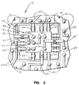
- FIGs. 1 and 2 there is shown an electronic package 10 in accordance with one embodiment of the invention.
- Package 10 comprises a first circuitized substrate 11, a second circuitized substrate 13 and a semiconductor device (chip) 15.
- Substrate 11 is preferably a printed circuit board (PCB) which, as is known, includes a dielectric material 17 with one or more conductive planes located therein and/or thereon. Such conductive planes typically provide signal, power and/or ground capabilities for the PCB, as is well known in the art. PCBs may include several such conductive planes spacedly positioned within the dielectric 17, as is also well known.
- substrate 17 includes at least one upper surface 19 having thereon a plurality of electrical conductors 21, in turn may provide signal capabilities for substrate 11 and thus package 10.
- Each of these conductors 21 is preferably of copper material as is known in the art. Conductors 21 may comprise flat pads or the like as is known or comprise circuit lines as is also known. Such conductors may also be electrically coupled (e.g., using plated through holes, not shown) to selected internal conductive planes (not shown), as is also known in the art.
- a substrate 11 having a thickness of about 0.060 inch and a total of four internal conductive planes (in addition to the illustrated external plane) was utilized.
- Second circuitized substrate 13 is substantially flexible and includes at least one dielectric layer 23 having at least one side (the lower side in Fig. 1) including a surface 25 having several electrical conducting elements 27 thereon. Substrate 13 is electrically coupled to substrate 11 in the manner defined below, such that selected ones of the conductive elements 27 are electrically connected to respective, selected ones of the electrical conductors 21. As defined below, solder is the chosen means to accomplish these connections.
- Substrate 13 is preferably comprised of a thin (e.g., 0.002 inch thick) polyimide dielectric layer (23) and the illustrated lower layer of conductive elements 27 on surface 25 are preferably of copper.
- a thin (e.g., 0.002 inch thick) polyimide dielectric layer (23) and the illustrated lower layer of conductive elements 27 on surface 25 are preferably of copper.
- polyimide and copper conductive elements for a flexible circuitized substrate are known in the art and further description is not believed necessary.
- each of the conductive elements 27 may comprise a metallic pad, similar to conductors 21, as well as a circuit line or the like.
- conductive elements designed to bridge respective apertures (described below) in substrate 13 are preferably copper leads which project across these apertures and are of substantially elongated configuration (Fig. 2).
- substrate 13 includes at least one aperture 31 therein which, as shown in Fig. 2, is of substantially continuous shape so as to substantially surround a segmented portion 33 of substrate 13.
- aperture 31 therein which, as shown in Fig. 2, is of substantially continuous shape so as to substantially surround a segmented portion 33 of substrate 13.
- individual apertures may be spacedly located within the substrates' polyimide layer in accordance with a predetermined pattern, each of the selected bridging leads thus bridging a respective one of such apertures.
- the respective bridging leads 27, whether located on a lower or upper surface (and thus on opposite sides) of substrate 13, serve to maintain segment 33 in a proper, aligned position relative to the remainder of the substrate.
- Flexible substrate 13 further preferably includes a second layer of conductive elements 27' on an opposing surface 25' opposite surface 25 having elements 27.
- Elements 27' may be of similar configuration to elements 27 and also of similar conductive materials. Additionally, it is also within the scope of the invention that elements 27' are connected to selected ones of elements 27, e.g., using plated-through-hole technology as is known in the art, one representative example illustrated in Fig. 1 by the numeral 35. All of the elements 27 and 27' may be interconnected through such conductive through holes, excluding those designated for bridging the aperture(s) 31. In Fig. 1, at least one conductive element 27' is shown to bridge the lower aperture. In Fig.
- bridging elements 27' are shown, as are several lower bridging conductors 27.
- the numbers of these bridging elements as shown in the drawings is not limiting of the invention, but provided only for representation purposes. In one embodiment of the invention a total of 60 lower bridging conductive elements 27 may be utilized while a comparative number of 560 such upper bridging conductive elements 27' are used.
- Chip 15 includes a plurality of contact sites 41 spacedly positioned along a bottom surface of the chip in accordance with a predetermined pattern. Such contact sites are known in the art and typically provided on semiconductor chips. In one example of the invention, a total of 620 such sites were provided for a chip used in the package structure of the present invention. It is understood that the sites 41 depicted in Fig. 2 are thus provided for representation purposes only and not meant to limit the invention.
- selected ones of the lower bridging conductive elements 27 of substrate 13 are thermocompression bonded to selected ones of the contact sites 41 on chip 15. Additionally, the upper bridging elements 27' are similarly attached, both of these attachments occurring, significantly, through the aperture(s) 41 in substrate 13. Of further significance, this relatively harsh means of attachment (thermal compression bonding) is accomplished following attachment of the solder elements (balls) to the lower conductive elements 27, as part of the procedure for making the present invention. This means of solder application is defined in greater detail herein below. Thermocompression bonding represents a known procedure in the microelectronics art and further description is thus not believed necessary.
- each of the bridging elements 27 and 27' is of substantially rectangular configuration and extends across the adjacent aperture(s) 31. Understandably, these are electrically connected to corresponding, respective conductive elements (27 or 27') to form the desired circuits including these elements.
- the invention is able to provide means for effectively coupling conductive elements on opposing surfaces of a flexible circuitized substrate to a chip, while also providing effective electrical coupling between these elements and respective conductors on a more rigid, other substrate (e.g., PCB) in such a manner that solder elements are effectively used, including, uniquely, immediately below the chip on a opposite side of the flexible substrate from the chips' position.
- a more rigid, other substrate e.g., PCB
- solder elements 51 may be used immediately below chip 15 on the segment 33 of substrate 13, in addition to several more solder elements 51 at remaining, selected portions of this substrate.
- solder elements 51 are initially affixed to selected ones of the lower conductors 27 using a procedure such as defined in detail in the aforementioned U.S. Patent 5,203,075 which patent, as stated, is incorporated herein by reference. Specifically, a solder paste (not shown) is preferably applied to these selected elements 27 and a spherical solder member (ball) is then positioned on the paste. Subsequently, heat is applied to cause the paste to "ball up" and solidify about the solder ball.
- the paste preferably being a 63:37 tin:lead solder, while the individual solder balls are 10:90 tin:lead solder members, these latter elements having a higher melting point than the paste to thus provide the several advantages taught in 5,203,075.
- paste may not necessarily be utilized but instead individual spherical solder elements (balls) aligned relative to the respective conductive elements and heat applied to cause partial deformation (melting) of the balls to thereby effect connection to elements 27.
- individual spherical solder elements balls
- heat applied to cause partial deformation (melting) of the balls to thereby effect connection to elements 27.
- Such a process may be similar to that defined in the aforementioned U.S. Patent 5,133,495, which is also incorporated herein by reference.
- Fig. 3 represents a flow diagram illustrating the various steps defined above.
- a significant feature of the present invention is the initial positioning of solder elements on designated conductive elements of a flexible substrate and thereafter subjecting this substrate, having said solder elements precisely positioned thereon, to a relatively harsh procedure (thermal compression bonding) such that others of such conductive elements will be soundly electrically connected to designated contact sites on a semiconductor device, thus allowing placement of selected ones of the solder elements 51 under (opposite) the semiconductor device as well as along the outer areas of the flexible circuit.
- Thermal compression bonding involves a single point bonding technique wherein the bonder will extend (project) into the respective apertures 31 to engage elements 27 (or 27') and effect connection with chip 15.
- this semiconductor device-flexible circuit subassembly is then aligned, relative to substrate 11 such that the solder elements 51 on substrate 13 are precisely oriented relative to respective conductors (21) on substrate 11.
- Such alignment is preferably accomplished by using a split optics placement tool commonly used in the industry during surface mount assembly operations.
- the solder elements 51 of the subassembly are positioned onto respective solder paste sites (the paste not shown in the drawings) in the manner defined in the aforementioned U.S. Patent 5,203,075. Heat is then effectively applied to this aligned structure to cause reflow (melting) of the solder paste so as to effect connection to the respective conductors 21.
- the solder paste is preferably 63:37 tin: lead and the reflow process accomplished at a temperature of about 200 degrees Celsius (C).
Landscapes
- Engineering & Computer Science (AREA)
- Manufacturing & Machinery (AREA)
- Microelectronics & Electronic Packaging (AREA)
- Wire Bonding (AREA)
- Combinations Of Printed Boards (AREA)
- Production Of Multi-Layered Print Wiring Board (AREA)
- Structures For Mounting Electric Components On Printed Circuit Boards (AREA)
Applications Claiming Priority (2)
| Application Number | Priority Date | Filing Date | Title |
|---|---|---|---|
| US08/153,734 US5367435A (en) | 1993-11-16 | 1993-11-16 | Electronic package structure and method of making same |
| US153734 | 1993-11-16 |
Publications (2)
| Publication Number | Publication Date |
|---|---|
| EP0653789A2 true EP0653789A2 (fr) | 1995-05-17 |
| EP0653789A3 EP0653789A3 (fr) | 1995-08-30 |
Family
ID=22548516
Family Applications (1)
| Application Number | Title | Priority Date | Filing Date |
|---|---|---|---|
| EP94115979A Withdrawn EP0653789A3 (fr) | 1993-11-16 | 1994-10-11 | Structure de boîtier électronique et sa fabrication. |
Country Status (3)
| Country | Link |
|---|---|
| US (1) | US5367435A (fr) |
| EP (1) | EP0653789A3 (fr) |
| JP (1) | JP2664873B2 (fr) |
Cited By (2)
| Publication number | Priority date | Publication date | Assignee | Title |
|---|---|---|---|---|
| DE19640225A1 (de) * | 1996-02-01 | 1997-08-07 | Mitsubishi Electric Corp | Halbleiteranordnung und Verfahren zu ihrer Herstellung |
| WO2021011286A1 (fr) | 2019-07-12 | 2021-01-21 | Neuralink Corp. | Schéma d'assemblage en sandwich pour réseau d'électrodes à film mince et circuits intégrés |
Families Citing this family (54)
| Publication number | Priority date | Publication date | Assignee | Title |
|---|---|---|---|---|
| US5834705A (en) * | 1994-03-04 | 1998-11-10 | Silicon Graphics, Inc. | Arrangement for modifying eletrical printed circuit boards |
| JP2833996B2 (ja) * | 1994-05-25 | 1998-12-09 | 日本電気株式会社 | フレキシブルフィルム及びこれを有する半導体装置 |
| JP2647001B2 (ja) * | 1994-05-31 | 1997-08-27 | 日本電気株式会社 | テープキャリアならびに半導体デバイスの実装構造およびその製造方法 |
| US5896276A (en) * | 1994-08-31 | 1999-04-20 | Nec Corporation | Electronic assembly package including connecting member between first and second substrates |
| US5778505A (en) * | 1994-10-04 | 1998-07-14 | Gemcor Engineering Corporation | Apparatus for fastening a semi-cylindrical workpiece |
| JPH08213422A (ja) * | 1995-02-07 | 1996-08-20 | Mitsubishi Electric Corp | 半導体装置およびそのボンディングパッド構造 |
| US5585162A (en) * | 1995-06-16 | 1996-12-17 | Minnesota Mining And Manufacturing Company | Ground plane routing |
| US5675183A (en) * | 1995-07-12 | 1997-10-07 | Dell Usa Lp | Hybrid multichip module and methods of fabricating same |
| US5976910A (en) * | 1995-08-30 | 1999-11-02 | Nec Corporation | Electronic device assembly and a manufacturing method of the same |
| MY123146A (en) * | 1996-03-28 | 2006-05-31 | Intel Corp | Perimeter matrix ball grid array circuit package with a populated center |
| US5808874A (en) * | 1996-05-02 | 1998-09-15 | Tessera, Inc. | Microelectronic connections with liquid conductive elements |
| US5774340A (en) * | 1996-08-28 | 1998-06-30 | International Business Machines Corporation | Planar redistribution structure and printed wiring device |
| US5759737A (en) * | 1996-09-06 | 1998-06-02 | International Business Machines Corporation | Method of making a component carrier |
| US5804771A (en) * | 1996-09-26 | 1998-09-08 | Intel Corporation | Organic substrate (PCB) slip plane "stress deflector" for flip chip deivces |
| JP3633252B2 (ja) | 1997-01-10 | 2005-03-30 | イビデン株式会社 | プリント配線板及びその製造方法 |
| AU5496098A (en) | 1997-01-23 | 1998-08-18 | Seiko Epson Corporation | Film carrier tape, semiconductor assembly, semiconductor device, manufacturing method therefor, mounting board, and electronic equipment |
| JPH10275966A (ja) * | 1997-01-30 | 1998-10-13 | Ibiden Co Ltd | プリント配線板及びその製造方法 |
| US5898219A (en) * | 1997-04-02 | 1999-04-27 | Intel Corporation | Custom corner attach heat sink design for a plastic ball grid array integrated circuit package |
| WO1998056219A1 (fr) * | 1997-06-06 | 1998-12-10 | Ibiden Co., Ltd. | Tableau de connexions imprime a couches multiples et procede de fabrication dudit tableau |
| US6730541B2 (en) * | 1997-11-20 | 2004-05-04 | Texas Instruments Incorporated | Wafer-scale assembly of chip-size packages |
| JP3971500B2 (ja) * | 1998-02-20 | 2007-09-05 | ソニー株式会社 | 半導体素子実装用配線基板の製造方法 |
| US6423623B1 (en) | 1998-06-09 | 2002-07-23 | Fairchild Semiconductor Corporation | Low Resistance package for semiconductor devices |
| US6414391B1 (en) | 1998-06-30 | 2002-07-02 | Micron Technology, Inc. | Module assembly for stacked BGA packages with a common bus bar in the assembly |
| US6133634A (en) | 1998-08-05 | 2000-10-17 | Fairchild Semiconductor Corporation | High performance flip chip package |
| US6050832A (en) * | 1998-08-07 | 2000-04-18 | Fujitsu Limited | Chip and board stress relief interposer |
| US6239485B1 (en) | 1998-11-13 | 2001-05-29 | Fujitsu Limited | Reduced cross-talk noise high density signal interposer with power and ground wrap |
| US6081026A (en) * | 1998-11-13 | 2000-06-27 | Fujitsu Limited | High density signal interposer with power and ground wrap |
| US6221694B1 (en) * | 1999-06-29 | 2001-04-24 | International Business Machines Corporation | Method of making a circuitized substrate with an aperture |
| DE19930308B4 (de) * | 1999-07-01 | 2006-01-12 | Infineon Technologies Ag | Multichipmodul mit Silicium-Trägersubstrat |
| US6281437B1 (en) | 1999-11-10 | 2001-08-28 | International Business Machines Corporation | Method of forming an electrical connection between a conductive member having a dual thickness substrate and a conductor and electronic package including said connection |
| US6264612B1 (en) | 2000-01-14 | 2001-07-24 | Children's Hospital Medical Center | Catheter with mechano-responsive element for sensing physiological conditions |
| US6624522B2 (en) * | 2000-04-04 | 2003-09-23 | International Rectifier Corporation | Chip scale surface mounted device and process of manufacture |
| US7057292B1 (en) | 2000-05-19 | 2006-06-06 | Flipchip International, Llc | Solder bar for high power flip chips |
| JP2002111233A (ja) * | 2000-10-03 | 2002-04-12 | Victor Co Of Japan Ltd | プリント配線板及びその製造方法 |
| US6930397B2 (en) | 2001-03-28 | 2005-08-16 | International Rectifier Corporation | Surface mounted package with die bottom spaced from support board |
| US7119447B2 (en) * | 2001-03-28 | 2006-10-10 | International Rectifier Corporation | Direct fet device for high frequency application |
| US7476964B2 (en) * | 2001-06-18 | 2009-01-13 | International Rectifier Corporation | High voltage semiconductor device housing with increased clearance between housing can and die for improved flux flushing |
| US6582990B2 (en) | 2001-08-24 | 2003-06-24 | International Rectifier Corporation | Wafer level underfill and interconnect process |
| US6784540B2 (en) | 2001-10-10 | 2004-08-31 | International Rectifier Corp. | Semiconductor device package with improved cooling |
| JP3678212B2 (ja) * | 2002-05-20 | 2005-08-03 | ウシオ電機株式会社 | 超高圧水銀ランプ |
| US7397137B2 (en) | 2002-07-15 | 2008-07-08 | International Rectifier Corporation | Direct FET device for high frequency application |
| US7579697B2 (en) | 2002-07-15 | 2009-08-25 | International Rectifier Corporation | Arrangement for high frequency application |
| US6755700B2 (en) * | 2002-11-12 | 2004-06-29 | Modevation Enterprises Inc. | Reset speed control for watercraft |
| US6841865B2 (en) * | 2002-11-22 | 2005-01-11 | International Rectifier Corporation | Semiconductor device having clips for connecting to external elements |
| US20050269677A1 (en) * | 2004-05-28 | 2005-12-08 | Martin Standing | Preparation of front contact for surface mounting |
| US7524701B2 (en) * | 2005-04-20 | 2009-04-28 | International Rectifier Corporation | Chip-scale package |
| US7230333B2 (en) | 2005-04-21 | 2007-06-12 | International Rectifier Corporation | Semiconductor package |
| US8466546B2 (en) | 2005-04-22 | 2013-06-18 | International Rectifier Corporation | Chip-scale package |
| US20060289981A1 (en) * | 2005-06-28 | 2006-12-28 | Nickerson Robert M | Packaging logic and memory integrated circuits |
| JP4795883B2 (ja) * | 2006-07-21 | 2011-10-19 | 株式会社日立ハイテクノロジーズ | パターン検査・計測装置 |
| US20080241563A1 (en) * | 2007-03-30 | 2008-10-02 | Khamvong Thammasouk | Polymer substrate for electronic components |
| JP5644264B2 (ja) * | 2009-10-14 | 2014-12-24 | 富士通株式会社 | 半導体装置 |
| US9742091B2 (en) * | 2014-04-11 | 2017-08-22 | R&D Sockets, Inc. | Method and structure for conductive elastomeric pin arrays using solder interconnects and a non-conductive medium |
| US10477684B2 (en) * | 2015-09-25 | 2019-11-12 | Intel Corporation | Apparatus, system, and method including a bridge device for interfacing a package device with a substrate |
Family Cites Families (27)
| Publication number | Priority date | Publication date | Assignee | Title |
|---|---|---|---|---|
| US3795047A (en) * | 1972-06-15 | 1974-03-05 | Ibm | Electrical interconnect structuring for laminate assemblies and fabricating methods therefor |
| JPS5269564A (en) * | 1975-12-08 | 1977-06-09 | Seiko Epson Corp | Semiconductor device and its manufacturing process |
| JPS5366166A (en) * | 1976-11-26 | 1978-06-13 | Hitachi Ltd | Electron part |
| US4413308A (en) * | 1981-08-31 | 1983-11-01 | Bell Telephone Laboratories, Incorporated | Printed wiring board construction |
| US4435740A (en) * | 1981-10-30 | 1984-03-06 | International Business Machines Corporation | Electric circuit packaging member |
| EP0152189A3 (fr) * | 1984-01-25 | 1987-12-09 | Luc Technologies Limited | Fixation de conducteurs électriques et dispositifs ainsi connectés |
| JPS6389280U (fr) * | 1986-12-01 | 1988-06-10 | ||
| US5159535A (en) * | 1987-03-11 | 1992-10-27 | International Business Machines Corporation | Method and apparatus for mounting a flexible film semiconductor chip carrier on a circuitized substrate |
| US5054192A (en) * | 1987-05-21 | 1991-10-08 | Cray Computer Corporation | Lead bonding of chips to circuit boards and circuit boards to circuit boards |
| US5195237A (en) * | 1987-05-21 | 1993-03-23 | Cray Computer Corporation | Flying leads for integrated circuits |
| US5045975A (en) * | 1987-05-21 | 1991-09-03 | Cray Computer Corporation | Three dimensionally interconnected module assembly |
| JPH0358537A (ja) * | 1989-07-27 | 1991-03-13 | Nikon Corp | カレントループ伝送装置 |
| US5135155A (en) * | 1989-08-25 | 1992-08-04 | International Business Machines Corporation | Thermocompression bonding in integrated circuit packaging |
| KR940004246B1 (ko) * | 1989-09-11 | 1994-05-19 | 신닛뽕 세이데쓰 가부시끼가이샤 | Tab 테이프와 반도체칩을 접속하는 방법 및 그것에 사용하는 범프시이트와 범프 부착 tab 테이프 |
| JP2753746B2 (ja) * | 1989-11-06 | 1998-05-20 | 日本メクトロン株式会社 | Ic搭載用可撓性回路基板及びその製造法 |
| US5127570A (en) * | 1990-06-28 | 1992-07-07 | Cray Research, Inc. | Flexible automated bonding method and apparatus |
| US5057969A (en) * | 1990-09-07 | 1991-10-15 | International Business Machines Corporation | Thin film electronic device |
| US5115964A (en) * | 1990-09-07 | 1992-05-26 | International Business Machines Corporation | Method for bonding thin film electronic device |
| US5148265A (en) * | 1990-09-24 | 1992-09-15 | Ist Associates, Inc. | Semiconductor chip assemblies with fan-in leads |
| JPH04154136A (ja) * | 1990-10-18 | 1992-05-27 | Fujitsu Ltd | ベアチップの実装方法 |
| US5133495A (en) * | 1991-08-12 | 1992-07-28 | International Business Machines Corporation | Method of bonding flexible circuit to circuitized substrate to provide electrical connection therebetween |
| US5203075A (en) * | 1991-08-12 | 1993-04-20 | Inernational Business Machines | Method of bonding flexible circuit to cicuitized substrate to provide electrical connection therebetween using different solders |
| JP2537325B2 (ja) * | 1991-11-29 | 1996-09-25 | 明 北原 | 表面実装電子部品と製法 |
| US5222014A (en) * | 1992-03-02 | 1993-06-22 | Motorola, Inc. | Three-dimensional multi-chip pad array carrier |
| EP0569949A3 (en) * | 1992-05-12 | 1994-06-15 | Akira Kitahara | Surface mount components and semifinished products thereof |
| JP3151219B2 (ja) * | 1992-07-24 | 2001-04-03 | テツセラ,インコーポレイテッド | 取り外し自在のリード支持体を備えた半導体接続構成体およびその製造方法 |
| JPH06291165A (ja) * | 1993-04-01 | 1994-10-18 | Nec Corp | フリップチップ接続構造 |
-
1993
- 1993-11-16 US US08/153,734 patent/US5367435A/en not_active Expired - Lifetime
-
1994
- 1994-08-31 JP JP6206560A patent/JP2664873B2/ja not_active Expired - Fee Related
- 1994-10-11 EP EP94115979A patent/EP0653789A3/fr not_active Withdrawn
Cited By (3)
| Publication number | Priority date | Publication date | Assignee | Title |
|---|---|---|---|---|
| DE19640225A1 (de) * | 1996-02-01 | 1997-08-07 | Mitsubishi Electric Corp | Halbleiteranordnung und Verfahren zu ihrer Herstellung |
| WO2021011286A1 (fr) | 2019-07-12 | 2021-01-21 | Neuralink Corp. | Schéma d'assemblage en sandwich pour réseau d'électrodes à film mince et circuits intégrés |
| EP3996802A4 (fr) * | 2019-07-12 | 2023-10-25 | Neuralink Corp. | Schéma d'assemblage en sandwich pour réseau d'électrodes à film mince et circuits intégrés |
Also Published As
| Publication number | Publication date |
|---|---|
| JPH07183333A (ja) | 1995-07-21 |
| JP2664873B2 (ja) | 1997-10-22 |
| US5367435A (en) | 1994-11-22 |
| EP0653789A3 (fr) | 1995-08-30 |
Similar Documents
| Publication | Publication Date | Title |
|---|---|---|
| US5367435A (en) | Electronic package structure and method of making same | |
| US5561323A (en) | Electronic package with thermally conductive support member having a thin circuitized substrate and semiconductor device bonded thereto | |
| US5773884A (en) | Electronic package with thermally conductive support member having a thin circuitized substrate and semiconductor device bonded thereto | |
| US5633533A (en) | Electronic package with thermally conductive support member having a thin circuitized substrate and semiconductor device bonded thereto | |
| US6420664B1 (en) | Metal foil having bumps, circuit substrate having the metal foil, and semiconductor device having the circuit substrate | |
| US5641113A (en) | Method for fabricating an electronic device having solder joints | |
| US5760469A (en) | Semiconductor device and semiconductor device mounting board | |
| KR0157284B1 (ko) | 솔더 볼 장착홈을 갖는 인쇄 회로 기판과 이를 사용한 볼 그리드 어레이 패키지 | |
| EP0594427B1 (fr) | Plaque à circuit imprimé avec des éléments électriques montés dessus | |
| US20020017398A1 (en) | Method for transforming a substrate with edge contacts into a ball grid array, ball grid array manufactured according to this method, and flexible wiring for the transformation of a substrate with edge contacts into a ball grid array | |
| JPH0767002B2 (ja) | 回路パッケージ構造 | |
| KR980006157A (ko) | 반도체패키지의 구조 및 제조방법 | |
| US6034437A (en) | Semiconductor device having a matrix of bonding pads | |
| US6656771B2 (en) | Semiconductor device, method of connecting a semiconductor chip, circuit board, and electronic equipment | |
| KR100510316B1 (ko) | 반도체 장치 및 그 제조방법, 회로기판 및 전자기기 | |
| JP2001168233A (ja) | 多重回線グリッド・アレイ・パッケージ | |
| JPH08191128A (ja) | 電子装置 | |
| US6281437B1 (en) | Method of forming an electrical connection between a conductive member having a dual thickness substrate and a conductor and electronic package including said connection | |
| KR100891652B1 (ko) | 반도체 칩 실장용 기판 | |
| JPS63122135A (ja) | 半導体チツプの電気的接続方法 | |
| JPH10256414A (ja) | 半導体パッケージ | |
| KR100246848B1 (ko) | 랜드 그리드 어레이 및 이를 채용한 반도체 패키지 | |
| JPH0645763A (ja) | 印刷配線板 | |
| KR100362502B1 (ko) | 가요성회로기판스트립을이용하여제조되는볼그리드어레이반도체패키지의싱글레이션방법및장치 | |
| JPH0751794Y2 (ja) | 半導体の実装構造 |
Legal Events
| Date | Code | Title | Description |
|---|---|---|---|
| PUAI | Public reference made under article 153(3) epc to a published international application that has entered the european phase |
Free format text: ORIGINAL CODE: 0009012 |
|
| AK | Designated contracting states |
Kind code of ref document: A2 Designated state(s): DE FR GB |
|
| PUAL | Search report despatched |
Free format text: ORIGINAL CODE: 0009013 |
|
| AK | Designated contracting states |
Kind code of ref document: A3 Designated state(s): DE FR GB |
|
| 17P | Request for examination filed |
Effective date: 19950907 |
|
| STAA | Information on the status of an ep patent application or granted ep patent |
Free format text: STATUS: THE APPLICATION HAS BEEN WITHDRAWN |
|
| 18W | Application withdrawn |
Withdrawal date: 19961029 |