EP0658936A2 - Dispositif semi-conducteur à couches multiples - Google Patents
Dispositif semi-conducteur à couches multiples Download PDFInfo
- Publication number
- EP0658936A2 EP0658936A2 EP94119864A EP94119864A EP0658936A2 EP 0658936 A2 EP0658936 A2 EP 0658936A2 EP 94119864 A EP94119864 A EP 94119864A EP 94119864 A EP94119864 A EP 94119864A EP 0658936 A2 EP0658936 A2 EP 0658936A2
- Authority
- EP
- European Patent Office
- Prior art keywords
- power supply
- region
- regions
- signal line
- area
- Prior art date
- Legal status (The legal status is an assumption and is not a legal conclusion. Google has not performed a legal analysis and makes no representation as to the accuracy of the status listed.)
- Withdrawn
Links
Images


Classifications
-
- H—ELECTRICITY
- H10—SEMICONDUCTOR DEVICES; ELECTRIC SOLID-STATE DEVICES NOT OTHERWISE PROVIDED FOR
- H10P—GENERIC PROCESSES OR APPARATUS FOR THE MANUFACTURE OR TREATMENT OF DEVICES COVERED BY CLASS H10
- H10P95/00—Generic processes or apparatus for manufacture or treatments not covered by the other groups of this subclass
-
- H—ELECTRICITY
- H10—SEMICONDUCTOR DEVICES; ELECTRIC SOLID-STATE DEVICES NOT OTHERWISE PROVIDED FOR
- H10W—GENERIC PACKAGES, INTERCONNECTIONS, CONNECTORS OR OTHER CONSTRUCTIONAL DETAILS OF DEVICES COVERED BY CLASS H10
- H10W20/00—Interconnections in chips, wafers or substrates
- H10W20/40—Interconnections external to wafers or substrates, e.g. back-end-of-line [BEOL] metallisations or vias connecting to gate electrodes
- H10W20/41—Interconnections external to wafers or substrates, e.g. back-end-of-line [BEOL] metallisations or vias connecting to gate electrodes characterised by their conductive parts
- H10W20/427—Power or ground buses
Definitions
- the invention relates to a semiconductor device, especially to a multilayer semiconductor device in which device regions are formed under a power supply line area and a signal line area.
- a conventional multilayer semiconductor device uses Bus-Line system of arrangement, in which a device region and a signal line region are arranged separately.
- another type of conventional multilayer semiconductor device including a device block located under a signal line region has been proposed.
- a Japanese Patent Publication, Kokai Heisei 2-284229 describes a bus-line type of semiconductor memory in which same phase of signal lines are arranged together to be a bunch so that next two signal lines in a bunch are arranged with a small space from each other but next two bunches are arranged with a large space from each other.
- This kind of arrangement can prevent a semiconductor circuit, to be mounted in the device, from mis-operating.
- an object of the invention is to provide an improved semiconductor device which can be miniaturized well.
- a semiconductor device includes first layer including first and second device regions, in which semiconductor devices are formed; and a second layer including a signal line region, a first power supply region, which is one selected between power source and ground, and a second power supply region which is the remaining of the power source and ground, the second power supply region being horizontally positioned between the signal line and first power supply regions.
- the first device region is positioned under both the first and second power supply regions.
- the second device region is positioned under the signal line region and the second power supply region.
- an additional power supply line is arranged in the signal line region to supply stable electric power to the second device region.
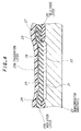
- Fig. 1 is a plane view illustrating the arrangement of a conventional semiconductor device.
- Fig. 2 is a cross-sectional view taken on line A-A in Fig. 1.
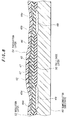
- Fig. 3 is a plane view illustrating the arrangement of a semiconductor device of a first preferred embodiment according to the invention.
- Fig. 4 is a cross-sectional view taken on line B-B in Fig. 3.
- Fig. 5 is a plane view illustrating the arrangement of a semiconductor device of a second preferred embodiment according to the invention.
- Fig. 6 is a cross-sectional view taken on line C-C in Fig. 5.
- Fig. 7 is a plane view illustrating the arrangement of a semiconductor device of a third preferred embodiment according to the invention.
- Fig. 8 is a cross-sectional view taken on line D-D in Fig. 7.
- FIGs. 1 and 2 show a conventional semiconductor device, including a semiconductor substrate 10, first and second device regions 11 and 12 formed on the semiconductor substrate 10, a field oxide layer 18, an insulation layer 19a, a passivation layer 19b, a power source line 14, a ground line 15, signal lines 16, connection lines 13 for connecting the power source line 14 and the ground line 15 to the second device region 12, and contact holes 17 for connecting the connection lines 13 to the signal lines 16, the power source line 14 and the ground line 15.
- the first and second device regions 11 and 12 are separated by the field oxide layer 18.
- the first device region 11 is arranged under both the power source line 14 and the ground line 15 so that stable electric power can be supplied to the first device region 11.
- the second device region 12 is connected to the power source line 14 and the ground line 15 via the connection lines 13 and the contact holes 17.
- Figs. 3 and 4 show a semiconductor device of a first preferred embodiment according to the invention, including a semiconductor substrate 20, first and second device regions 21 and 22 formed on the semiconductor substrate 20, a field oxide layer 28, an insulation layer 29a, a passivation layer 29b, a power source line 24, a ground line 25, signal lines 26, connection lines 23 for connecting the power source line 24 to the second device region 22, and contact holes 27 for connecting the connection lines 23 to the signal lines 26 and the power source line 24.
- the first and second device regions 21 and 22 are formed by separating a single device block so that the first device region 21 is designed larger than the second device region 22.
- a larger device for driving a large capacity of element and a smaller device, such as a delay circuit are to be mounted, respectively.
- the first device region 21 is arranged under both the power source line 24 and the ground line 25 so that stable electric power/ground level voltage can be supplied thereto directly.
- the second device region 22 is arranged under the signal lines 26 and the ground line 25 so that stable ground level voltage can be supplied thereto directly.
- Power source is provided from the power source line 24 through the connection line 23 and the contact hole 27 to the second device region 22.
- the same conductive type (P or N) of semiconductor elements are to be arranged.
- other device blocks may be arranged next to each of the first and second device regions 21 and 22.
- Figs. 5 and 6 show a semiconductor device of a second preferred embodiment according to the invention, including a semiconductor substrate 30, first and second device regions 31 and 32 formed on the semiconductor substrate 30, a field oxide layer 39a, an insulation layer 39b, a passivation layer 39c, power source lines 34 and 38, a ground line 35, signal lines 36, connection lines 33, and contact holes 27.
- the second preferred embodiment can be realized as a kind of modification of the first preferred embodiment.
- a feature of the second preferred embodiment is to arrange the additional power source line 38 in the signal lines 36 for providing stable power source to the second device region 32 without using connection lines.
- Figs. 7 and 8 show a semiconductor device of a third preferred embodiment according to the invention, including a semiconductor substrate 40, two first device regions 41a and 41b, two second device regions 42a and 42b, a field oxide layer 50, an insulation layer 52, a passivation layer 54, power source lines 44a, 44b and 48, two ground line 45a and 45b, signal lines 46, connection lines 43, and contact holes 47.
- the third preferred embodiment is fabricated by combining two devices according to the second preferred embodiment.
Landscapes
- Semiconductor Integrated Circuits (AREA)
- Design And Manufacture Of Integrated Circuits (AREA)
- Internal Circuitry In Semiconductor Integrated Circuit Devices (AREA)
Applications Claiming Priority (2)
| Application Number | Priority Date | Filing Date | Title |
|---|---|---|---|
| JP5314625A JP2876963B2 (ja) | 1993-12-15 | 1993-12-15 | 半導体装置 |
| JP314625/93 | 1993-12-15 |
Publications (2)
| Publication Number | Publication Date |
|---|---|
| EP0658936A2 true EP0658936A2 (fr) | 1995-06-21 |
| EP0658936A3 EP0658936A3 (fr) | 1996-03-27 |
Family
ID=18055567
Family Applications (1)
| Application Number | Title | Priority Date | Filing Date |
|---|---|---|---|
| EP94119864A Withdrawn EP0658936A3 (fr) | 1993-12-15 | 1994-12-15 | Dispositif semi-conducteur à couches multiples. |
Country Status (4)
| Country | Link |
|---|---|
| US (1) | US5517042A (fr) |
| EP (1) | EP0658936A3 (fr) |
| JP (1) | JP2876963B2 (fr) |
| KR (1) | KR100206080B1 (fr) |
Families Citing this family (8)
| Publication number | Priority date | Publication date | Assignee | Title |
|---|---|---|---|---|
| JP4027438B2 (ja) * | 1995-05-25 | 2007-12-26 | 三菱電機株式会社 | 半導体装置 |
| US6043551A (en) * | 1997-09-30 | 2000-03-28 | Intel Corporation | Metal locking structures to prevent a passivation layer from delaminating |
| US6215541B1 (en) | 1997-11-20 | 2001-04-10 | Samsung Electronics Co., Ltd. | Liquid crystal displays and manufacturing methods thereof |
| JP3913927B2 (ja) * | 1999-04-19 | 2007-05-09 | 富士通株式会社 | 半導体集積回路装置 |
| US6306745B1 (en) | 2000-09-21 | 2001-10-23 | Taiwan Semiconductor Manufacturing Company | Chip-area-efficient pattern and method of hierarchal power routing |
| US6759734B2 (en) * | 2001-03-15 | 2004-07-06 | Iolon, Inc. | Miniature device with increased insulative spacing and method for making same |
| KR100825012B1 (ko) | 2006-09-28 | 2008-04-24 | 주식회사 하이닉스반도체 | 저전력 소모를 위한 컬럼 디코더 |
| KR102770590B1 (ko) * | 2024-06-28 | 2025-02-19 | 이홍렬 | 전자파 차폐용 면상발열체 및 그 제어장치 |
Family Cites Families (11)
| Publication number | Priority date | Publication date | Assignee | Title |
|---|---|---|---|---|
| JPS5840344B2 (ja) * | 1980-06-10 | 1983-09-05 | 富士通株式会社 | 半導体記憶装置 |
| JPS5835963A (ja) * | 1981-08-28 | 1983-03-02 | Fujitsu Ltd | 集積回路装置 |
| JPS58157155A (ja) * | 1982-03-15 | 1983-09-19 | Ricoh Co Ltd | マスタスライスlsi |
| JPS60192359A (ja) * | 1984-03-14 | 1985-09-30 | Nec Corp | 半導体メモリ装置 |
| JPS60179042U (ja) * | 1984-05-09 | 1985-11-28 | シャープ株式会社 | ゲ−トアレイ半導体装置 |
| JPH0738414B2 (ja) * | 1987-01-09 | 1995-04-26 | 株式会社東芝 | 半導体集積回路 |
| JPH021928A (ja) * | 1988-06-10 | 1990-01-08 | Toshiba Corp | 半導体集積回路 |
| KR930003273B1 (ko) * | 1989-03-14 | 1993-04-24 | 가부시키가이샤 도시바 | 반도체장치 |
| JPH02284229A (ja) * | 1989-04-25 | 1990-11-21 | Nec Corp | マイクロプロセッサの状態記憶装置 |
| DE68925897T2 (de) * | 1989-04-28 | 1996-10-02 | Ibm | Gate-Array-Zelle, bestehend aus FET's von verschiedener und optimierter Grösse |
| JP3185271B2 (ja) * | 1991-09-13 | 2001-07-09 | 日本電気株式会社 | 半導体集積回路 |
-
1993
- 1993-12-15 JP JP5314625A patent/JP2876963B2/ja not_active Expired - Lifetime
-
1994
- 1994-12-13 US US08/354,556 patent/US5517042A/en not_active Expired - Lifetime
- 1994-12-14 KR KR1019940034217A patent/KR100206080B1/ko not_active Expired - Lifetime
- 1994-12-15 EP EP94119864A patent/EP0658936A3/fr not_active Withdrawn
Also Published As
| Publication number | Publication date |
|---|---|
| JPH07169840A (ja) | 1995-07-04 |
| KR100206080B1 (ko) | 1999-07-01 |
| US5517042A (en) | 1996-05-14 |
| EP0658936A3 (fr) | 1996-03-27 |
| KR950020965A (ko) | 1995-07-26 |
| JP2876963B2 (ja) | 1999-03-31 |
Similar Documents
| Publication | Publication Date | Title |
|---|---|---|
| US5838072A (en) | Intrachip power distribution package and method for semiconductors having a supply node electrically interconnected with one or more intermediate nodes | |
| EP0080361A2 (fr) | Dispositif de circuits intégrés du type à tranche maîtresse comprenant des semi-conducteurs métal-oxyde complémentaires | |
| EP0644594A1 (fr) | Configuration de lignes d'alimentation pour dispositif semi-conducteur | |
| US5726458A (en) | Hot carrier injection test structure and technique for statistical evaluation | |
| US6479845B2 (en) | Pattern for routing power and ground for an integrated circuit chip | |
| JP2001506429A (ja) | 半導体素子の電源/アース金属配線 | |
| US20060118866A1 (en) | Semiconductor device | |
| US5455460A (en) | Semiconductor device having complimentary bonding pads | |
| EP0658936A2 (fr) | Dispositif semi-conducteur à couches multiples | |
| US6114903A (en) | Layout architecture for core I/O buffer | |
| WO1984000252A1 (fr) | Acheminement d'un bus d'alimentation pour des reseaux de portes | |
| JPH0786430A (ja) | 半導体装置およびその製造方法 | |
| EP0399531A1 (fr) | Dispositif semi-conducteur à mémoire | |
| US7714447B2 (en) | Semiconductor chip arrangement | |
| JP4133600B2 (ja) | 半導体装置 | |
| KR100368699B1 (ko) | 반도체장치 | |
| EP0480611A2 (fr) | Dispositif de transistor à effet de champ pour la commutation d'un signal | |
| US5434436A (en) | Master-slice type semiconductor integrated circuit device having multi-power supply voltage | |
| EP0221431A2 (fr) | Interconnexions alignées entre étages logiques | |
| JPH1065146A (ja) | 半導体集積回路装置 | |
| JPH09172014A (ja) | 半導体装置の電源線構造 | |
| US5185652A (en) | Electrical connection between buses on a semiconductor integrated circuit | |
| US6841864B2 (en) | Semiconductor integrated circuit device, mounting board, and device and board assembly | |
| EP0571840A1 (fr) | Capteur d'images DTC multilinéaire | |
| EP0553726B1 (fr) | Circuit logique à semi-conducteurs |
Legal Events
| Date | Code | Title | Description |
|---|---|---|---|
| PUAI | Public reference made under article 153(3) epc to a published international application that has entered the european phase |
Free format text: ORIGINAL CODE: 0009012 |
|
| AK | Designated contracting states |
Kind code of ref document: A2 Designated state(s): DE FR GB |
|
| PUAL | Search report despatched |
Free format text: ORIGINAL CODE: 0009013 |
|
| AK | Designated contracting states |
Kind code of ref document: A3 Designated state(s): DE FR GB |
|
| 17P | Request for examination filed |
Effective date: 19960215 |
|
| 17Q | First examination report despatched |
Effective date: 19961223 |
|
| STAA | Information on the status of an ep patent application or granted ep patent |
Free format text: STATUS: THE APPLICATION HAS BEEN WITHDRAWN |
|
| 18W | Application withdrawn |
Withdrawal date: 19980602 |