EP0660390A2 - Structure d'isolation utilisant un dépôt d'oxyde en phase liquide - Google Patents
Structure d'isolation utilisant un dépôt d'oxyde en phase liquide Download PDFInfo
- Publication number
- EP0660390A2 EP0660390A2 EP94480153A EP94480153A EP0660390A2 EP 0660390 A2 EP0660390 A2 EP 0660390A2 EP 94480153 A EP94480153 A EP 94480153A EP 94480153 A EP94480153 A EP 94480153A EP 0660390 A2 EP0660390 A2 EP 0660390A2
- Authority
- EP
- European Patent Office
- Prior art keywords
- trench
- oxide
- recited
- layer
- resist
- Prior art date
- Legal status (The legal status is an assumption and is not a legal conclusion. Google has not performed a legal analysis and makes no representation as to the accuracy of the status listed.)
- Withdrawn
Links
Images

Classifications
-
- H—ELECTRICITY
- H10—SEMICONDUCTOR DEVICES; ELECTRIC SOLID-STATE DEVICES NOT OTHERWISE PROVIDED FOR
- H10W—GENERIC PACKAGES, INTERCONNECTIONS, CONNECTORS OR OTHER CONSTRUCTIONAL DETAILS OF DEVICES COVERED BY CLASS H10
- H10W10/00—Isolation regions in semiconductor bodies between components of integrated devices
-
- H—ELECTRICITY
- H10—SEMICONDUCTOR DEVICES; ELECTRIC SOLID-STATE DEVICES NOT OTHERWISE PROVIDED FOR
- H10W—GENERIC PACKAGES, INTERCONNECTIONS, CONNECTORS OR OTHER CONSTRUCTIONAL DETAILS OF DEVICES COVERED BY CLASS H10
- H10W10/00—Isolation regions in semiconductor bodies between components of integrated devices
- H10W10/01—Manufacture or treatment
- H10W10/011—Manufacture or treatment of isolation regions comprising dielectric materials
- H10W10/014—Manufacture or treatment of isolation regions comprising dielectric materials using trench refilling with dielectric materials, e.g. shallow trench isolations
-
- H—ELECTRICITY
- H10—SEMICONDUCTOR DEVICES; ELECTRIC SOLID-STATE DEVICES NOT OTHERWISE PROVIDED FOR
- H10P—GENERIC PROCESSES OR APPARATUS FOR THE MANUFACTURE OR TREATMENT OF DEVICES COVERED BY CLASS H10
- H10P14/00—Formation of materials, e.g. in the shape of layers or pillars
- H10P14/60—Formation of materials, e.g. in the shape of layers or pillars of insulating materials
- H10P14/63—Formation of materials, e.g. in the shape of layers or pillars of insulating materials characterised by the formation processes
- H10P14/6326—Deposition processes
- H10P14/6342—Liquid deposition, e.g. spin-coating, sol-gel techniques or spray coating
-
- H—ELECTRICITY
- H10—SEMICONDUCTOR DEVICES; ELECTRIC SOLID-STATE DEVICES NOT OTHERWISE PROVIDED FOR
- H10P—GENERIC PROCESSES OR APPARATUS FOR THE MANUFACTURE OR TREATMENT OF DEVICES COVERED BY CLASS H10
- H10P14/00—Formation of materials, e.g. in the shape of layers or pillars
- H10P14/60—Formation of materials, e.g. in the shape of layers or pillars of insulating materials
- H10P14/69—Inorganic materials
- H10P14/692—Inorganic materials composed of oxides, glassy oxides or oxide-based glasses
- H10P14/6921—Inorganic materials composed of oxides, glassy oxides or oxide-based glasses containing silicon
- H10P14/69215—Inorganic materials composed of oxides, glassy oxides or oxide-based glasses containing silicon the material being a silicon oxide, e.g. SiO2
-
- H—ELECTRICITY
- H10—SEMICONDUCTOR DEVICES; ELECTRIC SOLID-STATE DEVICES NOT OTHERWISE PROVIDED FOR
- H10W—GENERIC PACKAGES, INTERCONNECTIONS, CONNECTORS OR OTHER CONSTRUCTIONAL DETAILS OF DEVICES COVERED BY CLASS H10
- H10W10/00—Isolation regions in semiconductor bodies between components of integrated devices
- H10W10/01—Manufacture or treatment
-
- H—ELECTRICITY
- H10—SEMICONDUCTOR DEVICES; ELECTRIC SOLID-STATE DEVICES NOT OTHERWISE PROVIDED FOR
- H10W—GENERIC PACKAGES, INTERCONNECTIONS, CONNECTORS OR OTHER CONSTRUCTIONAL DETAILS OF DEVICES COVERED BY CLASS H10
- H10W10/00—Isolation regions in semiconductor bodies between components of integrated devices
- H10W10/10—Isolation regions comprising dielectric materials
- H10W10/17—Isolation regions comprising dielectric materials formed using trench refilling with dielectric materials, e.g. shallow trench isolations
Definitions
- the present invention generally relates to isolation structures in integrated circuits and, more particularly, to the formation of shallow trench isolation (STI) structures in integrated circuits having high integration density.
- STI shallow trench isolation
- Integrated circuits in which a plurality of interconnected circuit elements are formed on a single chip are now familiar in many types of electronic devices. Particularly in data processors, it has been recognized that the length of connections is a limiting factor in the reduction of processor cycle time and processor speed and, consequently, the incentive to include as many circuit components as possible on a single chip has been extremely strong. Additionally, if integrated circuit manufacturing yields for a chip design can be maintained at acceptable levels, a high degree of circuit integration yields substantial economies in the manufacture of electronic devices which include such integrated circuits. Therefore, the current trend in integrated circuit design is toward greater integration densities on each chip.
- Recessed oxide isolation may be of several different depths or aspect ratios depending on the anticipated type of circuit interaction.
- So-called deep trench structures usually have a relatively large aspect ratio (e.g. depth to width) of about 4:1 and have been quite effective to prevent electron movement within the bulk of a semiconductor substrate, principally in designs of bipolar devices and having feature size regimes which have been prevalent over the past few years.
- these type of structures cannot be scaled to feature sizes which are now possible at the current level of integrated circuit technology consistent with retaining their effectiveness for isolation and other device fabrication requirements.
- the formation of a "bird's beak” also causes a region of high stress to develop between the nitride mask and underlying layers and this high stress region can also encroach into the active device area beyond the region actually occupied by the "bird's beak". These high stress regions may be relieved after the device is placed in service by the formation of crystal dislocations that will be deleterious to the electrical characteristics of the device.
- STI shallow trench isolation
- a typical process sequence includes resist patterning, Reactive Ion Etching (RIE), with or without taper, to form a recess in the substrate, a channel stop implant at the bottom and sidewalls of the trench, stripping of the resist, oxidation of the substrate within the trench to form a sidewall oxide in the trench, a chemical vapor deposition (CVD) oxide fill, block-out resist patterning, a further dry etch for planarization, a chemical-mechanical polish and annealing of the oxide on the trench sidewall.
- This and similar known processes also tend to create high stress regions in the adjacent device areas which are eventually resolved by the spontaneous formation of dislocation loops in the crystal lattice of the semiconductor substrate. Charge leakage from devices formed in device areas of integrated circuits having STI structures has been associated with such dislocation loops.
- STI structures Another problem which has been encountered with STI structures is the process of filling narrow trenches with CVD oxide. Since the filling occurs somewhat conformally (e.g. deposition on trench sides may progress somewhat more slowly than on the trench bottom but usually the differential is less than the aspect ratio of the trench), voids can be formed by filling of the upper portion of the narrow trench before lower regions are filled. Further, even for STI structures where the trench aspect ratio is lower, the generally conformal deposition causes a surface void or dimple at the top of the trench which may complicate planarization by processes such as (wet) chemical and or mechanical polishing and also capture contaminants.
- LPD liquid phase deposition
- silicon oxide has been deposited on a surface at 35° C using a solution of flu- orosilicicacid (H 2 SiF 6 , sometimes referred to variously as hydrofluorosilicic acid, hydrohexafluorosilicic acid, hydrofluosilicic acid orfluosilicic acid) and boric acid (H 3 BO 3 ) which is supersaturated with silica (Si0 2 ), as disclosed in "A New Process for Silica Coating" by Hirotsuga Nagayama et al., published in the Journal of the Electrochemical Society, August, 1988, pp.2013 - 2016, which is fully incorporated by reference.
- solubility of silica is said to decrease with increasing temperature and a saturated solution can be made transiently supersaturated by increasing temperature or in other ways.
- the excess silica is then deposited on a surface immersed in the solution while the concentration of resulting hydrofluoric acid is minimized by reaction with the boric acid.
- the improvement in dielectric qualities of the oxide due to heat treatment causes densification and a reduction in volume of the deposited oxide which may cause stressing of the oxide and/or the material on which it is deposited.
- This stressing can be a source of lattice dislocations which can form charge traps or leaky paths between devices which are adjacent an isolation structure.
- annealing of the oxide and the development of improved dielectric qualities thereby cannot be exploited since stresses and dislocations are engendered.
- a semiconductor device including an insulating structure including a trench extending into a body of semiconductor material, a deposit of insulating oxide which has been deposited by liquid phase deposition substantially filling the trench, and a layer of thermally grown oxide at an interface of the body of semiconductor material and the deposit of insulating oxide in the trench.
- a method of forming an integrated circuit device including the steps of forming a trench extending into a body of semiconductor material, substantially filling the trench with an insulating oxide by a liquid phase deposition process, and heat treating the semiconductor material and insulating oxide in trench sufficiently to form a layer of thermal oxide at an interface of the body of semiconductor material and the insulating oxide.
- a method of forming a semiconductor structure including the steps of depositing silicon oxide on a semiconductor material from a supersaturated liquid phase solution containing silica, densifying silicon oxide deposited by the depositing step, and relieving stress at an interface between the silicon oxide and the semiconductor material by growing thermal oxide at the interface in volume sufficient to approximately compensate for change of volume of the silicon oxide during the densification step.
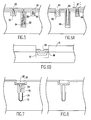
- a thin blanket layer of a hard polish-stop material such as an oxide/nitride composite material, has been deposited on substrate 12.
- a blanket photoresist layer 16 has also been deposited over the polish-stop material and exposed and the exposure pattern has been developed to form openings 18 in the resist.
- the polish-stop material is opened by a CF 4 reactive ion etch (RIE) and the shallow trench 18' formed by a C1 2 RIE.
- RIE reactive ion etch
- This patterning and the formation of the shallow trench 18' allows ion implantation to form a channel stop region 20 in a self-aligned manner which is well- understood in the art. It should also be understood that the formation of the structure in accordance with the invention is entirely independent of dopant and implant conductivity types which can be chosen and modified at will in dependence on the types of devices to be formed in the active device regions between the isolation trenches (e.g. to the right and/or the left of the exemplary isolation trench shown). It is also possible and may be advantageous in some circumstances to provide other structures on the substrate such as blanket layers or wells of semiconductor material of differing conductivity type and to form the isolation structure by forming the trench into the body of the semiconductor structure, whether or not the substrate is reached.
- the opening 18, 18' is partially filled by deposition of silicon oxide (e.g. silica) by liquid phase deposition from a supersaturated solution of silica in fluorosilicic acid, preferably containing an effective amount of boric acid to remove hydrofluoric acid which is formed during the oxide growth.
- silicon oxide e.g. silica
- fluorosilicic acid preferably containing an effective amount of boric acid to remove hydrofluoric acid which is formed during the oxide growth.
- boric acid to remove hydrofluoric acid which is formed during the oxide growth.
- the deposition process be continued until the oxide growth fills the shallow trench 18' and a significant portion of the opening 18 in the photoresist as shown at 22 of Figure 2.
- the growth of oxide is neither ideally conformal nor ideally isotropic; the growth rate from the sides of the trench being significantly less than the growth rate from the trench bottom, yielding a dimple 24 in the surface of the oxide deposit.
- this dimple 24 as well as the change of profile during densification (to the approximate profile shown at 22' of Figure 3) it is preferred to continue the oxide deposition until the bottom of the dimple is reliably raised above the plane of the upper surface of the polish-stop layer 14 by a distance greater than the change in dimple location during densification so that the dimple can be fully and reliably removed by planarization, as will be described more fully below.
- liquid phase deposition has been found, by the inventors, to proceed largely from the bottom of the trench with a much reduced deposition rate on the sides of the trench.
- deposition since the deposition is done from a supersaturated solution of silica, deposition occurs at the threshold of precipitation and is thus anisotropic, preferentially depositing a greater thickness in a direction perpendicular to the deposition surface.
- relatively open dimples 63, 65, 67 are formed which do not impede deposition at the bottom of the trench and are far less susceptible to retaining contaminants that the deep dimple 53 formed by CVD.
- Liquid phase deposition can also be performed with relatively high selectivity. If, as is preferred and shown in Figures 1 and 6B, a resist layer 16 is provided substantially congruent with the trench opening 61, deposition on the surfaces of the resist can be substantially or completely avoided during filling of the trench. Slow deposition on the sidewalls also retards growth of "shoulders" on the deposited oxide until the trench is substantially filled. Thereafter, as deposition continues into the thickness of the resist 16, deposition becomes more nearly conformal and results in only a shallow and open dimple 24, well above the substrate surface. It can therefore be clearly seen that liquid phase deposition is well-suited to the filling of trenches in isolation structures, particularly at very small sizes and is not limited to previously known applications such as conductor layer insulation. Moreover, the deposition profiles developed by liquid phase deposition significantly reduce the tendency to form voids and other defects which have been associated with the filling of small or high aspect ratio trenches by CVD.
- resist 16 is removed as shown in Figure 3 and the wafer is rinsed, dried and annealed in an oxygen furnace.
- the time and temperature of the annealing process is preferably determined as sufficient to grow a thin layer of oxide 30 at the interface of the substrate and the deposited oxide. (Approximately 100 Angstroms of thermal oxide is sufficient to provide electrical interface in terms of charge and interface states.
- Conditions of oxidation are relatively less important than temperature since interface charge densities are established by the annealing temperature to which the device was most recently exposed.)
- This thermal oxide is preferably grown in a post-anneal process at 800°C ⁇ 100°C for a period of 30 minutes + 15 minutes for an isolation structure formed in accordance with quarter-micron to half-micron design ground rules. While some annealing of the oxide will also take place, increasing density of the deposited oxide and reducing the dielectric constant, the annealing of the oxide has been found to be of lesser importance than the formation of the thermal oxide at the interface. (Also because of the densification of the deposited oxide, it is preferred that the deposition be continued to a point that the bottom of dimple 24 will remain at or above the plane of the upper surface of the polish-stop layer 14 after heat treatment.)
- the poor interface quality between the deposited oxide and the substrate has been found to form a charge trap which may eventually become conductive. That is, the interface may include charges and/or interface states which can induces channeling around the sidewalls of the trench. Therefore, the formation of the thermal oxide is considered to be important to the invention since it not only improves the interface quality by filling gaps and relieving dislocations which may form during the densification of the oxide but is believed to improve dielectric qualities of the oxide deposited by liquid phase deposition since the densification and oxygenation may eliminate voids and charge centers in addition to saturation of dangling bonds which can attract mobile charge and result in leaky paths between adjacent devices.
- Thermal oxidation will also compensate for any shrinkage of the LPD oxide caused by densification, preventing separation of trench fill from the sidewalls. Therefore, the electrical insulation and prevention of charge leakage provided by the isolation structure in accordance with the invention is principally a function of the thermal oxide grown during the heat treatment. Further, the growth of thermal oxide provides a mechanism of stress relief which is not available in other oxide deposition processes where the as-deposited oxide is relatively dense and residual stress must be tolerated. It is therefore preferred to grow thermal oxide to the point of minimizing stresses in the semiconductor device structure which also assures adequate thermal oxide thickness to produce good electrical properties.
- the isolation structure is completed by a light chemical-mechanical polish to remove the portion of the deposited oxide protruding above the surface of polish-stop layer 14 which is preferably provided to facilitate the polishing process and to avoid damage to the underlying body of semiconductor material (e.g. the substrate 12) to make the final upper surface 26 of the oxide deposit 24 coplanar with the upper surface of layer 14.
- a light chemical-mechanical polish to remove the portion of the deposited oxide protruding above the surface of polish-stop layer 14 which is preferably provided to facilitate the polishing process and to avoid damage to the underlying body of semiconductor material (e.g. the substrate 12) to make the final upper surface 26 of the oxide deposit 24 coplanar with the upper surface of layer 14.
- the methodology of the invention is also applicable to the formation of deep trench storage capacitors of small "footprint" such as are used in high capacity dynamic random access memories, which are familiar computer components.
- the structure of such capacitors including node oxide 72, a polycrystalline silicon plate 74 (poly- plate), a collar oxide 76 and a silicon cap 78, surrounded by thermal oxide, is generally familiar to those skilled in the art and the functions of these structural features need not be further described.
- Figure 7 shows a cross-section of a conventional deep trench capacitor formed by high-temperature chemical vapor deposition.
- the various structural features involve filling of trenches with material and the development of oxide at the interfaces of the deposits and the substrate.
- Two problems have been encountered with conventional depositions of materials in the deep trench which are similar to problems solved by the invention in isolation structures.
- the poly plate 74 and cap 78 will each have a seam 74' and 78', respectively, similar to the deep dimple 53 of Figure 5 and due to the same deposition mechanism previously described.
- thermal oxide is grown at the interfaces, thermal oxide is also grown at the seams which causes stresses which may later be resolved by formation of dislocations.
- high temperature deposition processes such as CVD, also create more stress-induced defects and dislocations.
- the improved filling by liquid phase deposition and densification by annealing avoids the production of a seam in which thermal oxide may grow. No stress-induced dislocations occur during deposition since deposition occurs at low temperature. Further, densification reduces the volume of the deposited material in a controlled, predictable and repeatable manner and stresses induced by the heat treatment are relieved and dislocations and voids filled by the growth of the thermal oxide. Further, as in the case of the isolation trench, the deposited oxide is of particularly good dielectric quality and increased dielectric constant, potentially allowing trench capacitors to be reduced in size without reduction of capacitance.
- the combination of low temperature deposition (with or without some degree of thermal densification) together with the growth of thermal oxide (which will, itself, cause some degree of densification, tending to reduce stresses which would otherwise be caused by thermal oxide growth) provides an insulative structure of improved performance, manufacturing yield and structural characteristics in a variety of structures which require filling of a trench-like feature.
- the invention provides a simple STI structure and method of formation thereof which involves only simple and self-aligned process steps which can be conducted with equipment of relatively low cost.
- the structure is easily planarized and is capable of filling relatively high aspect ratio trenches.
- the structure provides very low leakage and is very stable over time and electrical and thermal stress cycles since there is little stress induced in the structure by the liquid phase deposition process and that level of intrinsic stress can be maintained at a low level by choice of oxidation and heat treatment conditions by techniques which will be apparent to those skilled in the art in view of this description of the invention.
- the thermal cycle necessary to grow the thermal oxide 30 is very short and well within the "heat budgets" allowed for the formation of many types of devices and portions thereof as long as metallic conductors are not present. Since the process is entirely self-aligned after the initial resist exposure, the process and structure of the invention are fully compatible with any design rules and minimum feature sizes which can be achieved at any available level of lithographic technology and the available level of lithographic precision can be fully exploited.
- the invention is not limited to silicon substrates and that the silica deposited from the liquid phase allows the thermal growth of silicon oxide at an interface to substrates or layers of other materials such as germanium, indium and gallium/gallium arsenide.
Landscapes
- Element Separation (AREA)
- Formation Of Insulating Films (AREA)
- Metal-Oxide And Bipolar Metal-Oxide Semiconductor Integrated Circuits (AREA)
Applications Claiming Priority (2)
| Application Number | Priority Date | Filing Date | Title |
|---|---|---|---|
| US173396 | 1988-03-25 | ||
| US17339693A | 1993-12-23 | 1993-12-23 |
Publications (2)
| Publication Number | Publication Date |
|---|---|
| EP0660390A2 true EP0660390A2 (fr) | 1995-06-28 |
| EP0660390A3 EP0660390A3 (fr) | 1997-07-09 |
Family
ID=22631817
Family Applications (1)
| Application Number | Title | Priority Date | Filing Date |
|---|---|---|---|
| EP94480153A Withdrawn EP0660390A3 (fr) | 1993-12-23 | 1994-11-24 | Structure d'isolation utilisant un dépÔt d'oxyde en phase liquide. |
Country Status (7)
| Country | Link |
|---|---|
| US (1) | US5516721A (fr) |
| EP (1) | EP0660390A3 (fr) |
| JP (1) | JP2804446B2 (fr) |
| KR (1) | KR0167813B1 (fr) |
| BR (1) | BR9405158A (fr) |
| CA (1) | CA2131668C (fr) |
| TW (1) | TW265457B (fr) |
Cited By (5)
| Publication number | Priority date | Publication date | Assignee | Title |
|---|---|---|---|---|
| EP0959496A3 (fr) * | 1998-05-22 | 1999-12-15 | Applied Materials, Inc. | Procédé pour la fabrication d'une couche diélectrique auto-planarisée pour une rainure d'isolation |
| WO2001099172A1 (fr) * | 2000-06-23 | 2001-12-27 | Gemplus | Isolation electrique de tranches de puces par depot de sio2 en phase liquide |
| US6660615B1 (en) * | 1998-10-13 | 2003-12-09 | Windbond Electronics Corp. | Method and apparatus for growing layer on one surface of wafer |
| CN103632961A (zh) * | 2012-08-20 | 2014-03-12 | 上海华虹宏力半导体制造有限公司 | 功率mosfet芯片保护结构制造方法 |
| CN112366205A (zh) * | 2020-11-09 | 2021-02-12 | 长江存储科技有限责任公司 | 一种半导体器件及其制备方法 |
Families Citing this family (68)
| Publication number | Priority date | Publication date | Assignee | Title |
|---|---|---|---|---|
| US5516720A (en) * | 1994-02-14 | 1996-05-14 | United Microelectronics Corporation | Stress relaxation in dielectric before metallization |
| KR0134108B1 (ko) * | 1994-06-30 | 1998-04-20 | 김주용 | 반도체 소자의 제조방법 |
| US5530293A (en) | 1994-11-28 | 1996-06-25 | International Business Machines Corporation | Carbon-free hydrogen silsesquioxane with dielectric constant less than 3.2 annealed in hydrogen for integrated circuits |
| US5770501A (en) * | 1995-12-22 | 1998-06-23 | United Microelectronics Corporation | Process of fabricating NAND-structure flash EEPROM using liquid phase deposition |
| US6322634B1 (en) | 1997-01-27 | 2001-11-27 | Micron Technology, Inc. | Shallow trench isolation structure without corner exposure |
| TW337592B (en) * | 1997-04-03 | 1998-08-01 | Nat Science Council | Process of depositing silicon dioxide on a group III-V semiconductor substrate by ammoniation treatment |
| US5972570A (en) * | 1997-07-17 | 1999-10-26 | International Business Machines Corporation | Method of photolithographically defining three regions with one mask step and self aligned isolation structure formed thereby |
| US6013558A (en) * | 1997-08-06 | 2000-01-11 | Vlsi Technology, Inc. | Silicon-enriched shallow trench oxide for reduced recess during LDD spacer etch |
| US6455394B1 (en) * | 1998-03-13 | 2002-09-24 | Micron Technology, Inc. | Method for trench isolation by selective deposition of low temperature oxide films |
| US6150072A (en) * | 1997-08-22 | 2000-11-21 | Siemens Microelectronics, Inc. | Method of manufacturing a shallow trench isolation structure for a semiconductor device |
| US7157385B2 (en) * | 2003-09-05 | 2007-01-02 | Micron Technology, Inc. | Method of depositing a silicon dioxide-comprising layer in the fabrication of integrated circuitry |
| US6087243A (en) * | 1997-10-21 | 2000-07-11 | Advanced Micro Devices, Inc. | Method of forming trench isolation with high integrity, ultra thin gate oxide |
| US5952707A (en) * | 1997-12-05 | 1999-09-14 | Stmicroelectronics, Inc. | Shallow trench isolation with thin nitride as gate dielectric |
| US6211002B1 (en) * | 1998-01-28 | 2001-04-03 | Texas Instruments-Acer Incorporated | CMOS process for forming planarized twin wells |
| KR100283469B1 (ko) * | 1998-06-08 | 2001-04-02 | 윤종용 | 반도체소자제조방법 |
| US6239002B1 (en) * | 1998-10-19 | 2001-05-29 | Taiwan Semiconductor Manufacturing Company | Thermal oxidizing method for forming with attenuated surface sensitivity ozone-teos silicon oxide dielectric layer upon a thermally oxidized silicon substrate layer |
| US6120607A (en) * | 1998-12-03 | 2000-09-19 | Lsi Logic Corporation | Apparatus and method for blocking the deposition of oxide on a wafer |
| US6140208A (en) * | 1999-02-05 | 2000-10-31 | International Business Machines Corporation | Shallow trench isolation (STI) with bilayer of oxide-nitride for VLSI applications |
| JP3439388B2 (ja) * | 1999-07-27 | 2003-08-25 | 日本電気株式会社 | 半導体装置の製造方法 |
| US6300219B1 (en) * | 1999-08-30 | 2001-10-09 | Micron Technology, Inc. | Method of forming trench isolation regions |
| US6221735B1 (en) * | 2000-02-15 | 2001-04-24 | Philips Semiconductors, Inc. | Method for eliminating stress induced dislocations in CMOS devices |
| US6271100B1 (en) | 2000-02-24 | 2001-08-07 | International Business Machines Corporation | Chemically enhanced anneal for removing trench stress resulting in improved bipolar yield |
| US6348394B1 (en) | 2000-05-18 | 2002-02-19 | International Business Machines Corporation | Method and device for array threshold voltage control by trapped charge in trench isolation |
| US6429061B1 (en) * | 2000-07-26 | 2002-08-06 | International Business Machines Corporation | Method to fabricate a strained Si CMOS structure using selective epitaxial deposition of Si after device isolation formation |
| US6613641B1 (en) * | 2001-01-17 | 2003-09-02 | International Business Machines Corporation | Production of metal insulator metal (MIM) structures using anodizing process |
| US6605506B2 (en) * | 2001-01-29 | 2003-08-12 | Silicon-Based Technology Corp. | Method of fabricating a scalable stacked-gate flash memory device and its high-density memory arrays |
| WO2002101818A2 (fr) * | 2001-06-08 | 2002-12-19 | Amberwave Systems Corporation | Procede d'isolation de dispositifs semi-conducteurs |
| JP2005504436A (ja) | 2001-09-21 | 2005-02-10 | アンバーウェーブ システムズ コーポレイション | 画定された不純物勾配を有するひずみ材料層を使用する半導体構造、およびその構造を製作するための方法。 |
| AU2002341803A1 (en) * | 2001-09-24 | 2003-04-07 | Amberwave Systems Corporation | Rf circuits including transistors having strained material layers |
| US7060633B2 (en) * | 2002-03-29 | 2006-06-13 | Texas Instruments Incorporated | Planarization for integrated circuits |
| KR100864845B1 (ko) * | 2002-07-03 | 2008-10-23 | 매그나칩 반도체 유한회사 | 반도체소자의 소자분리막 제조방법 |
| US6593221B1 (en) * | 2002-08-13 | 2003-07-15 | Micron Technology, Inc. | Selective passivation of exposed silicon |
| US6960781B2 (en) * | 2003-03-07 | 2005-11-01 | Amberwave Systems Corporation | Shallow trench isolation process |
| US6767786B1 (en) * | 2003-04-14 | 2004-07-27 | Nanya Technology Corporation | Method for forming bottle trenches by liquid phase oxide deposition |
| TWI222180B (en) * | 2003-04-29 | 2004-10-11 | Nanya Technology Corp | Method for forming vertical transistor and trench capacitor |
| US7125815B2 (en) * | 2003-07-07 | 2006-10-24 | Micron Technology, Inc. | Methods of forming a phosphorous doped silicon dioxide comprising layer |
| US7273794B2 (en) * | 2003-12-11 | 2007-09-25 | International Business Machines Corporation | Shallow trench isolation fill by liquid phase deposition of SiO2 |
| US7053010B2 (en) * | 2004-03-22 | 2006-05-30 | Micron Technology, Inc. | Methods of depositing silicon dioxide comprising layers in the fabrication of integrated circuitry, methods of forming trench isolation, and methods of forming arrays of memory cells |
| US9257302B1 (en) | 2004-03-25 | 2016-02-09 | Novellus Systems, Inc. | CVD flowable gap fill |
| US7582555B1 (en) | 2005-12-29 | 2009-09-01 | Novellus Systems, Inc. | CVD flowable gap fill |
| US7074690B1 (en) * | 2004-03-25 | 2006-07-11 | Novellus Systems, Inc. | Selective gap-fill process |
| US7524735B1 (en) | 2004-03-25 | 2009-04-28 | Novellus Systems, Inc | Flowable film dielectric gap fill process |
| US7235459B2 (en) * | 2004-08-31 | 2007-06-26 | Micron Technology, Inc. | Methods of forming trench isolation in the fabrication of integrated circuitry, methods of fabricating memory circuitry, integrated circuitry and memory integrated circuitry |
| US7087531B1 (en) * | 2005-01-17 | 2006-08-08 | International Business Machines Corporation | Shallow trench isolation formation |
| US7510966B2 (en) * | 2005-03-07 | 2009-03-31 | Micron Technology, Inc. | Electrically conductive line, method of forming an electrically conductive line, and method of reducing titanium silicide agglomeration in fabrication of titanium silicide over polysilicon transistor gate lines |
| US8012847B2 (en) | 2005-04-01 | 2011-09-06 | Micron Technology, Inc. | Methods of forming trench isolation in the fabrication of integrated circuitry and methods of fabricating integrated circuitry |
| US7482215B2 (en) | 2006-08-30 | 2009-01-27 | International Business Machines Corporation | Self-aligned dual segment liner and method of manufacturing the same |
| US7888273B1 (en) | 2006-11-01 | 2011-02-15 | Novellus Systems, Inc. | Density gradient-free gap fill |
| US9245739B2 (en) | 2006-11-01 | 2016-01-26 | Lam Research Corporation | Low-K oxide deposition by hydrolysis and condensation |
| US7795605B2 (en) * | 2007-06-29 | 2010-09-14 | International Business Machines Corporation | Phase change material based temperature sensor |
| US20090072355A1 (en) * | 2007-09-17 | 2009-03-19 | International Business Machines Corporation | Dual shallow trench isolation structure |
| CN101452873B (zh) * | 2007-12-06 | 2010-08-11 | 上海华虹Nec电子有限公司 | 浅沟槽隔离工艺方法 |
| US8557712B1 (en) | 2008-12-15 | 2013-10-15 | Novellus Systems, Inc. | PECVD flowable dielectric gap fill |
| US8278224B1 (en) | 2009-09-24 | 2012-10-02 | Novellus Systems, Inc. | Flowable oxide deposition using rapid delivery of process gases |
| US8105956B2 (en) | 2009-10-20 | 2012-01-31 | Micron Technology, Inc. | Methods of forming silicon oxides and methods of forming interlevel dielectrics |
| TWI579916B (zh) | 2009-12-09 | 2017-04-21 | 諾菲勒斯系統公司 | 整合可流動氧化物及頂蓋氧化物之新穎間隙填充 |
| US8685867B1 (en) | 2010-12-09 | 2014-04-01 | Novellus Systems, Inc. | Premetal dielectric integration process |
| US9719169B2 (en) | 2010-12-20 | 2017-08-01 | Novellus Systems, Inc. | System and apparatus for flowable deposition in semiconductor fabrication |
| US8846536B2 (en) | 2012-03-05 | 2014-09-30 | Novellus Systems, Inc. | Flowable oxide film with tunable wet etch rate |
| US9847222B2 (en) | 2013-10-25 | 2017-12-19 | Lam Research Corporation | Treatment for flowable dielectric deposition on substrate surfaces |
| US10049921B2 (en) | 2014-08-20 | 2018-08-14 | Lam Research Corporation | Method for selectively sealing ultra low-k porous dielectric layer using flowable dielectric film formed from vapor phase dielectric precursor |
| US9916977B2 (en) | 2015-11-16 | 2018-03-13 | Lam Research Corporation | Low k dielectric deposition via UV driven photopolymerization |
| US10388546B2 (en) | 2015-11-16 | 2019-08-20 | Lam Research Corporation | Apparatus for UV flowable dielectric |
| JP6573575B2 (ja) * | 2016-05-02 | 2019-09-11 | 東京エレクトロン株式会社 | 凹部の埋め込み方法 |
| FR3067854B1 (fr) * | 2017-06-16 | 2019-08-02 | Universite De Tours Francois Rabelais | Realisation par voie liquide de revetements conformes de materiaux oxydes sur des substrats micro- ou macro-structures |
| CN113728415B (zh) | 2019-04-19 | 2025-05-16 | 朗姆研究公司 | 原子层沉积期间的快速冲洗清扫 |
| DE102020130617B4 (de) * | 2020-11-19 | 2025-03-06 | Infineon Technologies Ag | Halbleiterpackages mit elektrischen Umverteilungsschichten unterschiedlicher Dicken und Verfahren zu deren Herstellung |
| TWI809806B (zh) * | 2022-04-01 | 2023-07-21 | 南亞科技股份有限公司 | 半導體結構及其製造方法 |
Family Cites Families (16)
| Publication number | Priority date | Publication date | Assignee | Title |
|---|---|---|---|---|
| US4104086A (en) * | 1977-08-15 | 1978-08-01 | International Business Machines Corporation | Method for forming isolated regions of silicon utilizing reactive ion etching |
| US4544576A (en) * | 1981-07-27 | 1985-10-01 | International Business Machines Corporation | Deep dielectric isolation by fused glass |
| DE3332995A1 (de) * | 1983-07-14 | 1985-01-24 | Nippon Sheet Glass Co. Ltd., Osaka | Verfahren zum herstellen einer siliciumdioxidbeschichtung |
| JPS61207029A (ja) * | 1985-03-11 | 1986-09-13 | Nec Corp | 半導体集積回路装置 |
| JPS61281047A (ja) * | 1985-06-06 | 1986-12-11 | Nippon Sheet Glass Co Ltd | 二酸化珪素被膜の製造方法 |
| JPH01143254A (ja) * | 1987-11-28 | 1989-06-05 | Mitsubishi Electric Corp | 半導体記憶装置 |
| US4851370A (en) * | 1987-12-28 | 1989-07-25 | American Telephone And Telegraph Company, At&T Bell Laboratories | Fabricating a semiconductor device with low defect density oxide |
| JPH01295438A (ja) * | 1988-05-24 | 1989-11-29 | Matsushita Electric Ind Co Ltd | 半導体装置の製造方法 |
| US5270276A (en) * | 1989-04-25 | 1993-12-14 | Shell Oil Company | Process for the production of elastomeric, primarily syndiotactic polypropylene and catalysts for use in said process |
| JPH04106954A (ja) * | 1990-08-24 | 1992-04-08 | Sony Corp | 液相cvd法を用いた半導体装置の製造方法 |
| JPH04132240A (ja) * | 1990-09-21 | 1992-05-06 | Nippon Steel Corp | 半導体装置の製造方法 |
| JPH04245662A (ja) * | 1991-01-31 | 1992-09-02 | Matsushita Electric Ind Co Ltd | 半導体装置の製造方法 |
| KR960012587B1 (ko) * | 1991-10-01 | 1996-09-23 | 니뽄 덴끼 가부시끼가이샤 | 비대칭적으로 얇게 도핑된 드레인-금속 산화물 반도체 전계효과 트랜지스터(ldd-mosfet) 제조 방법 |
| JPH05102136A (ja) * | 1991-10-03 | 1993-04-23 | Toshiba Corp | 半導体集積回路装置の製造方法 |
| JPH05235157A (ja) * | 1992-02-26 | 1993-09-10 | Fujitsu Ltd | 半導体装置の製造方法 |
| JPH07122627A (ja) * | 1993-10-22 | 1995-05-12 | Sony Corp | 半導体装置の製造方法 |
-
1994
- 1994-09-08 CA CA002131668A patent/CA2131668C/fr not_active Expired - Fee Related
- 1994-11-24 EP EP94480153A patent/EP0660390A3/fr not_active Withdrawn
- 1994-12-05 JP JP6300507A patent/JP2804446B2/ja not_active Expired - Lifetime
- 1994-12-19 KR KR1019940034941A patent/KR0167813B1/ko not_active Expired - Fee Related
- 1994-12-20 BR BR9405158A patent/BR9405158A/pt not_active Application Discontinuation
-
1995
- 1995-02-23 US US08/393,599 patent/US5516721A/en not_active Expired - Fee Related
- 1995-03-23 TW TW084102817A patent/TW265457B/zh active
Cited By (6)
| Publication number | Priority date | Publication date | Assignee | Title |
|---|---|---|---|---|
| EP0959496A3 (fr) * | 1998-05-22 | 1999-12-15 | Applied Materials, Inc. | Procédé pour la fabrication d'une couche diélectrique auto-planarisée pour une rainure d'isolation |
| US6660615B1 (en) * | 1998-10-13 | 2003-12-09 | Windbond Electronics Corp. | Method and apparatus for growing layer on one surface of wafer |
| WO2001099172A1 (fr) * | 2000-06-23 | 2001-12-27 | Gemplus | Isolation electrique de tranches de puces par depot de sio2 en phase liquide |
| CN103632961A (zh) * | 2012-08-20 | 2014-03-12 | 上海华虹宏力半导体制造有限公司 | 功率mosfet芯片保护结构制造方法 |
| CN103632961B (zh) * | 2012-08-20 | 2016-08-10 | 上海华虹宏力半导体制造有限公司 | 功率mosfet芯片保护结构制造方法 |
| CN112366205A (zh) * | 2020-11-09 | 2021-02-12 | 长江存储科技有限责任公司 | 一种半导体器件及其制备方法 |
Also Published As
| Publication number | Publication date |
|---|---|
| TW265457B (fr) | 1995-12-11 |
| JP2804446B2 (ja) | 1998-09-24 |
| CA2131668A1 (fr) | 1995-06-24 |
| BR9405158A (pt) | 1995-08-01 |
| EP0660390A3 (fr) | 1997-07-09 |
| KR0167813B1 (ko) | 1999-02-01 |
| KR950021405A (ko) | 1995-07-26 |
| US5516721A (en) | 1996-05-14 |
| CA2131668C (fr) | 1999-03-02 |
| JPH07201979A (ja) | 1995-08-04 |
Similar Documents
| Publication | Publication Date | Title |
|---|---|---|
| US5516721A (en) | Isolation structure using liquid phase oxide deposition | |
| US5902127A (en) | Methods for forming isolation trenches including doped silicon oxide | |
| US5801082A (en) | Method for making improved shallow trench isolation with dielectric studs for semiconductor integrated circuits | |
| US5640041A (en) | Stress relaxation in dielectric before metallization | |
| US5445989A (en) | Method of forming device isolation regions | |
| US7858492B2 (en) | Method of filling a trench and method of forming an isolating layer structure using the same | |
| US5308786A (en) | Trench isolation for both large and small areas by means of silicon nodules after metal etching | |
| US6277709B1 (en) | Method of forming shallow trench isolation structure | |
| US5294562A (en) | Trench isolation with global planarization using flood exposure | |
| US20010006839A1 (en) | Method for manufacturing shallow trench isolation in semiconductor device | |
| US5565376A (en) | Device isolation technology by liquid phase deposition | |
| KR100251280B1 (ko) | 샐로우 트랜치 아이솔레이션 방법 | |
| KR0157875B1 (ko) | 반도체 장치의 제조방법 | |
| US5849625A (en) | Planar field oxide isolation process for semiconductor integrated circuit devices using liquid phase deposition | |
| US6503802B2 (en) | Method of fabricating isolation structure for semiconductor device | |
| US6103581A (en) | Method for producing shallow trench isolation structure | |
| US6344374B1 (en) | Method of fabricating insulators for isolating electronic devices | |
| US20040108524A1 (en) | Semiconductor device and method of manufacturing the same | |
| KR100419754B1 (ko) | 반도체소자의 소자분리막 형성방법 | |
| KR100558032B1 (ko) | 반도체 소자의 트렌치 소자분리 방법 | |
| KR100345521B1 (ko) | 트랜지스터의 게이트 형성 방법 | |
| KR100236720B1 (ko) | 반도체장치의 소자분리방법 | |
| KR100519648B1 (ko) | 반도체 소자의 제조 방법 | |
| KR100578239B1 (ko) | 반도체장치의 소자분리막 형성방법 | |
| KR100559134B1 (ko) | 반도체 장치의 소자 분리체 및 그 형성방법 |
Legal Events
| Date | Code | Title | Description |
|---|---|---|---|
| PUAI | Public reference made under article 153(3) epc to a published international application that has entered the european phase |
Free format text: ORIGINAL CODE: 0009012 |
|
| AK | Designated contracting states |
Kind code of ref document: A2 Designated state(s): BE CH DE FR GB IT LI NL SE |
|
| 17P | Request for examination filed |
Effective date: 19951024 |
|
| PUAL | Search report despatched |
Free format text: ORIGINAL CODE: 0009013 |
|
| AK | Designated contracting states |
Kind code of ref document: A3 Designated state(s): BE CH DE FR GB IT LI NL SE |
|
| STAA | Information on the status of an ep patent application or granted ep patent |
Free format text: STATUS: THE APPLICATION HAS BEEN WITHDRAWN |
|
| 18W | Application withdrawn |
Withdrawal date: 19971229 |