EP0660520A2 - Transistor à effet de champ MOS à blocage de courant bidirectionnel pour sectionneur de batterie comportant une protection contre la connexion inverse d'un chargeur de batterie - Google Patents
Transistor à effet de champ MOS à blocage de courant bidirectionnel pour sectionneur de batterie comportant une protection contre la connexion inverse d'un chargeur de batterie Download PDFInfo
- Publication number
- EP0660520A2 EP0660520A2 EP94309140A EP94309140A EP0660520A2 EP 0660520 A2 EP0660520 A2 EP 0660520A2 EP 94309140 A EP94309140 A EP 94309140A EP 94309140 A EP94309140 A EP 94309140A EP 0660520 A2 EP0660520 A2 EP 0660520A2
- Authority
- EP
- European Patent Office
- Prior art keywords
- mosfet
- region
- gate
- switch
- terminal
- Prior art date
- Legal status (The legal status is an assumption and is not a legal conclusion. Google has not performed a legal analysis and makes no representation as to the accuracy of the status listed.)
- Granted
Links
Images








Classifications
-
- H—ELECTRICITY
- H10—SEMICONDUCTOR DEVICES; ELECTRIC SOLID-STATE DEVICES NOT OTHERWISE PROVIDED FOR
- H10D—INORGANIC ELECTRIC SEMICONDUCTOR DEVICES
- H10D84/00—Integrated devices formed in or on semiconductor substrates that comprise only semiconducting layers, e.g. on Si wafers or on GaAs-on-Si wafers
- H10D84/101—Integrated devices comprising main components and built-in components, e.g. IGBT having built-in freewheel diode
- H10D84/141—VDMOS having built-in components
- H10D84/146—VDMOS having built-in components the built-in components being Schottky barrier diodes
-
- H—ELECTRICITY
- H02—GENERATION; CONVERSION OR DISTRIBUTION OF ELECTRIC POWER
- H02J—ELECTRIC POWER NETWORKS; CIRCUIT ARRANGEMENTS OR SYSTEMS FOR SUPPLYING OR DISTRIBUTING ELECTRIC POWER; SYSTEMS FOR STORING ELECTRIC ENERGY
- H02J1/00—Circuit arrangements for DC mains or DC distribution networks
- H02J1/10—Parallel operation of DC sources
-
- H—ELECTRICITY
- H02—GENERATION; CONVERSION OR DISTRIBUTION OF ELECTRIC POWER
- H02J—ELECTRIC POWER NETWORKS; CIRCUIT ARRANGEMENTS OR SYSTEMS FOR SUPPLYING OR DISTRIBUTING ELECTRIC POWER; SYSTEMS FOR STORING ELECTRIC ENERGY
- H02J7/00—Circuit arrangements for charging or discharging batteries or for supplying loads from batteries
- H02J7/50—Circuit arrangements for charging or discharging batteries or for supplying loads from batteries acting upon multiple batteries simultaneously or sequentially
- H02J7/575—Parallel/serial switching of connection of batteries to charge or load circuit
-
- H—ELECTRICITY
- H02—GENERATION; CONVERSION OR DISTRIBUTION OF ELECTRIC POWER
- H02J—ELECTRIC POWER NETWORKS; CIRCUIT ARRANGEMENTS OR SYSTEMS FOR SUPPLYING OR DISTRIBUTING ELECTRIC POWER; SYSTEMS FOR STORING ELECTRIC ENERGY
- H02J7/00—Circuit arrangements for charging or discharging batteries or for supplying loads from batteries
- H02J7/60—Circuit arrangements for charging or discharging batteries or for supplying loads from batteries including safety or protection arrangements
- H02J7/663—Circuit arrangements for charging or discharging batteries or for supplying loads from batteries including safety or protection arrangements using battery or load disconnect circuits
-
- H—ELECTRICITY
- H02—GENERATION; CONVERSION OR DISTRIBUTION OF ELECTRIC POWER
- H02J—ELECTRIC POWER NETWORKS; CIRCUIT ARRANGEMENTS OR SYSTEMS FOR SUPPLYING OR DISTRIBUTING ELECTRIC POWER; SYSTEMS FOR STORING ELECTRIC ENERGY
- H02J7/00—Circuit arrangements for charging or discharging batteries or for supplying loads from batteries
- H02J7/60—Circuit arrangements for charging or discharging batteries or for supplying loads from batteries including safety or protection arrangements
- H02J7/68—Circuit arrangements for charging or discharging batteries or for supplying loads from batteries including safety or protection arrangements using circuits for correcting or protecting against reverse-polarity
-
- H—ELECTRICITY
- H02—GENERATION; CONVERSION OR DISTRIBUTION OF ELECTRIC POWER
- H02J—ELECTRIC POWER NETWORKS; CIRCUIT ARRANGEMENTS OR SYSTEMS FOR SUPPLYING OR DISTRIBUTING ELECTRIC POWER; SYSTEMS FOR STORING ELECTRIC ENERGY
- H02J9/00—Circuit arrangements for emergency or stand-by power supply, e.g. for emergency lighting
- H02J9/04—Circuit arrangements for emergency or stand-by power supply, e.g. for emergency lighting in which the distribution system is disconnected from the normal source and connected to a standby source
- H02J9/06—Circuit arrangements for emergency or stand-by power supply, e.g. for emergency lighting in which the distribution system is disconnected from the normal source and connected to a standby source with automatic change-over, e.g. UPS systems
- H02J9/061—Circuit arrangements for emergency or stand-by power supply, e.g. for emergency lighting in which the distribution system is disconnected from the normal source and connected to a standby source with automatic change-over, e.g. UPS systems for DC powered loads
-
- H—ELECTRICITY
- H03—ELECTRONIC CIRCUITRY
- H03K—PULSE TECHNIQUE
- H03K17/00—Electronic switching or gating, i.e. not by contact-making and –breaking
- H03K17/08—Modifications for protecting switching circuit against overcurrent or overvoltage
- H03K17/082—Modifications for protecting switching circuit against overcurrent or overvoltage by feedback from the output to the control circuit
- H03K17/0822—Modifications for protecting switching circuit against overcurrent or overvoltage by feedback from the output to the control circuit in field-effect transistor switches
-
- H—ELECTRICITY
- H03—ELECTRONIC CIRCUITRY
- H03K—PULSE TECHNIQUE
- H03K17/00—Electronic switching or gating, i.e. not by contact-making and –breaking
- H03K17/51—Electronic switching or gating, i.e. not by contact-making and –breaking characterised by the components used
- H03K17/56—Electronic switching or gating, i.e. not by contact-making and –breaking characterised by the components used by the use, as active elements, of semiconductor devices
- H03K17/687—Electronic switching or gating, i.e. not by contact-making and –breaking characterised by the components used by the use, as active elements, of semiconductor devices the devices being field-effect transistors
-
- H—ELECTRICITY
- H03—ELECTRONIC CIRCUITRY
- H03K—PULSE TECHNIQUE
- H03K17/00—Electronic switching or gating, i.e. not by contact-making and –breaking
- H03K17/51—Electronic switching or gating, i.e. not by contact-making and –breaking characterised by the components used
- H03K17/56—Electronic switching or gating, i.e. not by contact-making and –breaking characterised by the components used by the use, as active elements, of semiconductor devices
- H03K17/687—Electronic switching or gating, i.e. not by contact-making and –breaking characterised by the components used by the use, as active elements, of semiconductor devices the devices being field-effect transistors
- H03K17/6871—Electronic switching or gating, i.e. not by contact-making and –breaking characterised by the components used by the use, as active elements, of semiconductor devices the devices being field-effect transistors the output circuit comprising more than one controlled field-effect transistor
- H03K17/6874—Electronic switching or gating, i.e. not by contact-making and –breaking characterised by the components used by the use, as active elements, of semiconductor devices the devices being field-effect transistors the output circuit comprising more than one controlled field-effect transistor in a symmetrical configuration
-
- H—ELECTRICITY
- H03—ELECTRONIC CIRCUITRY
- H03K—PULSE TECHNIQUE
- H03K17/00—Electronic switching or gating, i.e. not by contact-making and –breaking
- H03K17/51—Electronic switching or gating, i.e. not by contact-making and –breaking characterised by the components used
- H03K17/56—Electronic switching or gating, i.e. not by contact-making and –breaking characterised by the components used by the use, as active elements, of semiconductor devices
- H03K17/687—Electronic switching or gating, i.e. not by contact-making and –breaking characterised by the components used by the use, as active elements, of semiconductor devices the devices being field-effect transistors
- H03K17/693—Switching arrangements with several input- or output-terminals, e.g. multiplexers, distributors
-
- H—ELECTRICITY
- H10—SEMICONDUCTOR DEVICES; ELECTRIC SOLID-STATE DEVICES NOT OTHERWISE PROVIDED FOR
- H10D—INORGANIC ELECTRIC SEMICONDUCTOR DEVICES
- H10D30/00—Field-effect transistors [FET]
- H10D30/60—Insulated-gate field-effect transistors [IGFET]
-
- H—ELECTRICITY
- H10—SEMICONDUCTOR DEVICES; ELECTRIC SOLID-STATE DEVICES NOT OTHERWISE PROVIDED FOR
- H10D—INORGANIC ELECTRIC SEMICONDUCTOR DEVICES
- H10D30/00—Field-effect transistors [FET]
- H10D30/60—Insulated-gate field-effect transistors [IGFET]
- H10D30/601—Insulated-gate field-effect transistors [IGFET] having lightly-doped drain or source extensions, e.g. LDD IGFETs or DDD IGFETs
-
- H—ELECTRICITY
- H10—SEMICONDUCTOR DEVICES; ELECTRIC SOLID-STATE DEVICES NOT OTHERWISE PROVIDED FOR
- H10D—INORGANIC ELECTRIC SEMICONDUCTOR DEVICES
- H10D30/00—Field-effect transistors [FET]
- H10D30/60—Insulated-gate field-effect transistors [IGFET]
- H10D30/64—Double-diffused metal-oxide semiconductor [DMOS] FETs
- H10D30/645—Bidirectional devices
-
- H—ELECTRICITY
- H10—SEMICONDUCTOR DEVICES; ELECTRIC SOLID-STATE DEVICES NOT OTHERWISE PROVIDED FOR
- H10D—INORGANIC ELECTRIC SEMICONDUCTOR DEVICES
- H10D30/00—Field-effect transistors [FET]
- H10D30/60—Insulated-gate field-effect transistors [IGFET]
- H10D30/64—Double-diffused metal-oxide semiconductor [DMOS] FETs
- H10D30/66—Vertical DMOS [VDMOS] FETs
-
- H—ELECTRICITY
- H03—ELECTRONIC CIRCUITRY
- H03K—PULSE TECHNIQUE
- H03K2217/00—Indexing scheme related to electronic switching or gating, i.e. not by contact-making or -breaking covered by H03K17/00
- H03K2217/0018—Special modifications or use of the back gate voltage of a FET
-
- H—ELECTRICITY
- H10—SEMICONDUCTOR DEVICES; ELECTRIC SOLID-STATE DEVICES NOT OTHERWISE PROVIDED FOR
- H10D—INORGANIC ELECTRIC SEMICONDUCTOR DEVICES
- H10D84/00—Integrated devices formed in or on semiconductor substrates that comprise only semiconducting layers, e.g. on Si wafers or on GaAs-on-Si wafers
- H10D84/80—Integrated devices formed in or on semiconductor substrates that comprise only semiconducting layers, e.g. on Si wafers or on GaAs-on-Si wafers characterised by the integration of at least one component covered by groups H10D12/00 or H10D30/00, e.g. integration of IGFETs
- H10D84/82—Integrated devices formed in or on semiconductor substrates that comprise only semiconducting layers, e.g. on Si wafers or on GaAs-on-Si wafers characterised by the integration of at least one component covered by groups H10D12/00 or H10D30/00, e.g. integration of IGFETs of only field-effect components
- H10D84/83—Integrated devices formed in or on semiconductor substrates that comprise only semiconducting layers, e.g. on Si wafers or on GaAs-on-Si wafers characterised by the integration of at least one component covered by groups H10D12/00 or H10D30/00, e.g. integration of IGFETs of only field-effect components of only insulated-gate FETs [IGFET]
Definitions
- This invention relates to a bidirectional current blocking MOSFET and in particular to the use of such a device in a battery disconnect circuit.
- a primary battery B1 and a secondary battery B2 are connected via switches S1 and S2, respectively, to a load L, which could be a DC/DC converter supplying, for example, a notebook computer.
- the supply connections are made through a bus which is designated B.
- a backup battery B4 is also connected to bus B.
- Backup battery B4 provides power to some supervisory circuits and memory functions (not shown) when primary battery B1 and secondary battery B2 are discharged. To ensure that it is present when needed, backup battery B4 is not switched.
- switches S1, S2, and S3 In the operation of this multiple battery arrangement, only one of switches S1, S2, and S3 would normally be closed at any given time. The remaining switches would be open. When power is supplied by primary battery B1, for example, switch S1 is closed and switches S2 and S3 are open.
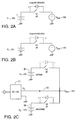
- the voltage across switches S1, S2, and S3 can vary both in magnitude and direction.- This is illustrated in Figs. 2A-2C.
- the output V2 of battery B2 might be 14 V at a given point in time. If battery B2 is then supplying power, the voltage V bus would also equal 14 V. If battery B1 is fully charged, its output voltage V1 might be 18 V. In this case, the left side of switch S1 would be positively charged. On the other hand, assume the same situation except that battery B1 is discharged, so that V1 is 6 V. In this case, the right side of switch S1 is positively charged, as shown in Fig. 2B.
- a third alternative is illustrated in Fig.
- V1 is shown as equalling 6 V
- V2 is shown as equalling 17 V
- V3 is shown as equalling 12 V.
- the right side of switch S1 is positively charged
- the left side of switch S2 is positively charged.
- any of switches S1-S3 may have to withstand a voltage in either direction. The only thing known for certain is that all of the voltages applied to these switches will be above ground.
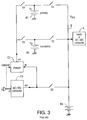
- the device may also be equipped with an internal battery charger, as illustrated in Fig. 3.
- a battery charger C5 is connected to battery B1 via a switch S4 and to battery B2 via a switch S5.
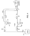
- Battery charger C5 may be supplied from the output of AC/DC converter C3 or (optionally) directly from the power main. As illustrated in Fig. 4, battery charger C5 may deliver a voltage as high as 24 V for quick battery charging. In the condition illustrated in Fig. 4, battery B2 is being charged, and the V1 output of battery B1 is equal to 12 volts. Switch S4 therefore must withstand a voltage difference of 12 V.
- switches S4 and S5 must also be bidirectional current blocking.
- switches S1-S5 were mechanical switches.
- MOSFETs are typically fabricated with a source-body short to ensure that the intrinsic bipolar transistor (represented by the source, body and drain regions) remains turned off at all times.
- the prior art teaches generally that a good source-body short is fundamental to reliable parasitic-bipolar-free power MOSFET operation. See, for example, "Power Integrated Circuits", by Paolo Antognetti, McGraw-Hill, 1986, pp. 3.27-3.34.
- a source-body short has the effect of creating a diode across the drain and body terminals of the MOSFET which is electrically in parallel with the MOSFET.
- the cathode of the diode is connected to the drain; for an N-channel device, the anode of the diode is connected to the drain.
- a MOSFET must never be exposed to voltages at its source-body and drain terminals which would cause the "antiparallel" diode to become forward-biased.
- Figs. 5A-5D illustrate the polarity of the antiparallel diode (shown in hatched lines) for a vertical N-channel DMOS device (Fig. 5A), a vertical P-channel DMOS device (Fig. 5B), a lateral N-channel device (Fig. 5C), and a lateral N-channel DMOS device (Fig. 5D).
- switches S1-S5 are not capable of blocking bidirectional currents.
- Figs. 2A-2C for example, the antiparallel diodes across switches S1 and S2 are shown in hatched lines, with their anode and cathode terminals arranged so as would be required to block the flow of current through the switches. If the polarity of the voltages across the switches were reversed, the antiparallel diodes would become forward-biased.
- Figs. 6A-6C illustrate a back-to-back arrangement
- Fig. 6A illustrates a pair of NMOS devices having a common source
- Fig. 6B illustrates a pair of NMOS devices having a common drain
- Fig. 6C illustrates a pair of PMOS devices having a common source.
- the connections between the battery charger and the battery may become reversed.
- some of the connectors used for battery chargers have interchangeable polarities, and some battery chargers contain a switch which allows the polarity of the output to be reversed. In such situations, a battery disconnect switch may be exposed to a negative rather than a positive voltage.
- bidirectional current blocking semiconductor switch which has the on-resistance of a normal MOSFET and yet does not contain an antiparallel diode across its drain and body terminals.
- the bidirectional current blocking semiconductor switch should also be able to withstand a reversed battery charger condition.
- a power MOSFET in accordance with this invention, includes a source region, a body region, a drain region and a gate, each of which is connected to a terminal.
- the source and body regions are not shorted together, and voltages that are applied to the source and drain terminals are both either higher than (for an N-channel device) or lower than (for a P-channel device) a voltage at which the body region is maintained.
- the source, body and drain voltages are established such that the source-body and drain-body junctions of the device are never forward-biased.
- the device is a four-terminal N-channel MOSFET, the body region is grounded, and the voltages at the source and drain terminals are never allowed to fall below ground. Thus, the junctions between the P-type body region and the N-type source and drain regions never become forward biased. Provided that the gate voltage transitions which turn the device on and off are fast and the load is relatively capacitive or resistive (but not inductive), the parasitic bipolar transistor represented by the source, body and drain regions will not be activated.
- the on-resistance of a device according to this invention is dramatically lower than either an N-channel DMOS AC switch or a P-channel DMOS AC switch (frequently referred to as a bilateral switch).
- a bidirectional blocking switch is capable of conducting current in either direction and is capable of blocking current whether the source is more positive than the drain or the drain is more positive than the source. Moreover, the switch of this invention is capable of inhibiting current between two voltages provided by two different power sources. Neither the source terminal nor the drain terminal need be tied to a fixed or regulated voltage. When the switch is turned on, it quickly pulls the voltage on each side to approximately the same level. (In this specification, the terms "source” and “drain” are frequently used to denote the terminals of the MOSFET even though either terminal may be more positive than the other.)
- a battery disconnect switch is protected against exposure to a negative voltage created by, for example, a reverse-connected battery charger.
- a pair of source-body shorted MOSFETs are connected back-to-back in series between the gate and source terminals of the battery disconnect switch (the source terminal of the switch being connected to the battery charger).
- the gates of the series-connected MOSFETs are grounded.
- a third source-body shorted MOSFET is connected between the body and source terminals of the battery disconnect switch.
- the gate of the third MOSFET is connected to the drain terminal of the battery disconnect switch (the drain terminal of the switch being connected to the battery).
- a MOSFET not having a source-body short is substituted for the back-to-back MOSFETs.
- Fig. 1 illustrates a schematic drawing of a multiple source power supply arrangement, including disconnect switches.
- Figs. 2A, 2B and 2C illustrate possible voltage differences encountered by the disconnect switches shown in Fig. 1.
- Fig. 3 illustrates a schematic diagram of a multiple source power supply arrangement, including a battery charger.
- Fig. 4 illustrates possible voltage differences encountered by the disconnect switches shown in Fig. 3.
- Figs. 5A-5D illustrate, respectively, a vertical N-channel double-diffused MOSFET (DMOS), a vertical P-channel DMOS MOSFET, a lateral N-channel MOSFET, and a lateral N-channel DMOS MOSFET, all of which contain a source-body short.
- DMOS vertical N-channel double-diffused MOSFET
- P-channel DMOS MOSFET vertical P-channel DMOS MOSFET
- a lateral N-channel MOSFET a lateral N-channel MOSFET
- a lateral N-channel DMOS MOSFET all of which contain a source-body short.
- Figs. 6A-6C illustrate bidirectional current blocking switches consisting of back-to-back MOSFETs.
- Fig. 7 illustrates a multiple source power supply arrangement containing disconnect switches in accordance with the invention.
- Fig. 8 illustrates schematically the general case of a switch according to this invention.
- Fig. 9 illustrates a multiple source power supply arrangement with disconnect switches consisting of drifted MOSFETs which are capable of switching higher voltage differences.
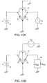
- Figs. 10A and 10B illustrate schematically the off-state and the on-state, respectively, of the switches illustrated in Figs. 7 and 8.
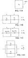
- Figs. 11A-11D illustrate conceptually the reduced on-resistance which is obtained using a bidirectional blocking switch in accordance with this invention.
- Fig. 12A illustrates a battery disconnect switch with no protection against a reversed battery charger
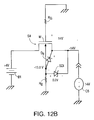
- Figs. 12B-12G illustrate the difficulties with several possible ways of protecting a battery disconnect switch against a reversed battery charger.
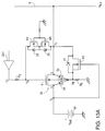
- Figs. 13A-13E illustrate a battery disconnect switch including circuitry which protects the switch against a reversed battery charger, in several voltage conditions to which the battery disconnect switch may be exposed.
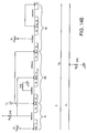
- Figs. 14A and 14B illustrate an embodiment in which the battery disconnect switch and the circuitry protecting the switch against a reversed battery charger are fabricated in the form of an integrated circuit.
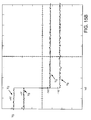
- Figs. 15A and 15B illustrate test results of the protective circuitry.
- Fig. 7 illustrates a multiple source power supply arrangement containing bidirectional current blocking switches 70 and 71 in accordance with the invention.
- Switch 70 is connected to a battery 72, which supplies a voltage V1
- switch 71 is connected to an AC/DC converter 73 or another battery, which supplies a voltage V2.
- Switches 70 and 71 connect into a bus 74, which supplies an output voltage V out to a load. While two power sources and two switches are illustrated in Fig. 7, it will be apparent that any number of batteries or other power sources could be included in the arrangement.
- Switch 70 is a lateral MOSFET which is illustrated in cross section.
- MOSFET 70 is preferably formed in either a stripe or cellular pattern in a substrate 75, which in this embodiment is formed of P-type semiconductor material.
- N+ regions 76 and 77 are formed at the surface of P substrate 75, separated by a channel region 78.
- a gate 79 is formed over channel region 78, separated from channel region 78 by an oxide layer 80.
- a terminal 81 connects N+ region 76 to battery 72 and a terminal 82 connects N+ region 77 to bus 74.
- Gate 79 is supplied by a gate voltage V G1 .
- switch 70 is a symmetrical device, and regions 76 and 77 are not referred to as source or drain regions, since either of them can be biased positively or negatively relative to each other.
- junction between P substrate 75 and N+ region 76 is represented by a dio D1 and the junction between P substrate 75 and N+ region 77 is represented by a diode D2.
- the gate voltage V G1 is held low when switch 70 is turned off, and is raised to a positive voltage when switch 70 is turned on. Since P substrate 75 is grounded, and since the voltage at terminals 81 and 82 can only be positive, it is apparent that one of diodes D1 and D2 is always reverse-biased when switch 70 is turned off. Accordingly, when switch 70 is off it blocks current whether the voltage at terminal 81 is higher or lower than the voltage at terminal 82.
- N+ region 76 nor N+ region 77 is shorted to P substrate 75.
- the NPN transistor represented by N+ regions 76 and 77 and P substrate 75 will not become activated, provided that the on-off transitions at gate 79 are fast relative to the reaction time (capacitance) of the load. Since this circuit acts like a follower, i.e., a common drain configuration relative to the most positive side, an on-state bipolar transistor immediately develops a reverse-biased source voltage which keeps the bipolar transistor turned off. In other words, at the onset of conduction, the formation of the channel in the MOSFET causes the voltage on both sides of the MOSFET to normalize to approximately the same voltage.
- the more negative potential will rise to a voltage near the positive value when the switch is activated.
- the beginning of conduction will immediately raise the more negative potential to a voltage above ground, thereby reverse-biasing the junction.
- the gate should be driven rapidly to minimize the duration of the switching transition.
- N+ terminal i.e., source or drain
- Another distinguishing characteristic is its possible connection to voltage sources of limited energy, such as batteries, where voltage decays with time.
- the bidirectional blocking switch is therefore not a "high side” switch (permanently tied to a fixed positive supply rail, present whenever circuit operation is desired), since batteries and even AC adapters may discharge or be unplugged. Likewise, it is not a “low side” switch because neither side is tied permanently to ground. Instead, it acts like a reversible source follower when conducting, with the more positive voltage acting as the drain and the more negative voltage as the source.
- Switch 71 is identical to switch 70 but has terminals designated 83 and 84 and is controlled by a gate voltage V G2 .
- switches 70 and 71 will block currents whenever their respective gate voltages V G1 and V G2 are low, provided that the voltage differences across the switch remain below the breakdown voltage of the internal diodes.
- the breakdown voltages of the internal diodes would normally be in the range of 8 V to 12 V to 14 V.
- Switches 70 and 71 can therefore be controlled to selectively connect or isolate battery 72 and AC/DC converter 73 without concern that an antiparallel diode in the switches will become forward-biased. Switches of this invention can be used for any of switches S1-S5 shown in Figs. 1 and 4.
- switches 70 and 71 appear in cross section to be conventional lateral N-channel MOSFETS, each of them has a large gate width W in order to achieve a low on-resistance, typically below 200 m ⁇ and as low as 60 m ⁇ .
- W gate width
- switches 70 and 71 appear in cross section to be conventional lateral N-channel MOSFETS, each of them has a large gate width W in order to achieve a low on-resistance, typically below 200 m ⁇ and as low as 60 m ⁇ .
- it is not common to subject both the source and drain terminals to voltages originating from more than one power source, nor is it common to operate a conventional MOSFET as a bi-directional source follower, i.e., without specifying which terminal acts as the higher (drain) terminal (in an NMOS device) which supplies current and which terminal acts as the lower (source) terminal, which sinks current to ground through a load.
- Fig. 8 illustrates schematically the general case of a switch S0 according to this invention connected between power sources P10 and P20.
- Power sources P10 and P20 generate voltages V10 and V20.
- Switch S0 will block current whether V10 > V20 or V20 > V10, and will conduct current from P10 to P20 or from P20 to P10.
- Source P20 may be disconnected entirely from the circuit via a second switch S0'.
- Fig. 9 illustrates a drifted version of switches 70 and 71, which is capable of withstanding higher voltage differences (for example, 15 V, 18 V or 24 V).
- a switch 90 contains N-drift regions 92 and 93, which serve to limit the strength of the electric field across oxide region 94. Drift regions are described more fully in U.S. Patent No. 5,237,193, to Williams, issued August 17, 1993, which is incorporated herein by reference. Since the gate must be biased sufficiently positive relative to ground to allow the device to conduct over the specified operating range, the oxide separating the gate from the channel region must be thick enough to accommodate the maximum gate voltage reliably. Since either side of switch 90 may serve as the "drain" in a given situation, a drift region must be provided on both sides of the channel region.
- the drifted embodiment illustrated in Fig. 9 is useful if the voltage across the switch is above about 14 V. In such situations the drift region prevents the gate oxide from exposure to high electric fields.
- the gate voltage of switch 90 may either be fixed or may be a voltage slightly higher than V1. If the gate voltage is a fixed value relative to ground (for example, 30 V) a standard gate oxide thickness (200-400 ⁇ ) will not support the gate-to-substrate bias at the moment of turn on, and a thicker gate (for example, over 700 ⁇ ) must be used. If the gate potential is limited to 10 V above the more negative terminal voltage and rises with that voltage, then the thicker oxide is not needed.
- Figs. 10A and 10B illustrate an example of the two states of switch 70 shown in Fig. 7.
- the gate of switch 70 is grounded and switch 70 is turned off, isolating battery 72 from AC/DC converter 73. This would be the situation, for example, when AC/DC converter is supplying the load. Assuming that V2 is greater than V1, diode D2 blocks current from flowing through switch 70.
- Fig. 10B illustrates the situation when the gate of switch 70 is biased at least one volt above ground. Switch 70 is then turned on, allowing battery 72 to supply a load 95, which includes a capacitance C load and resistance R load .
- Figs. 11A-11D illustrate a further advantage of bidirectional current blocking switches in accordance with this invention, namely, their significantly improved on-resistance.
- Fig. 11A shows an area A which represents the surface area of a lateral or vertical N-channel MOSFET.
- the on-resistance associated with the area A is designated R n , which is typically 1 milliohm for each square cm in area A.
- R n is typically 1 milliohm for each square cm in area A.
- a single P-channel device exhibits a resistance which is approximately 2.5R n because of hole mobility which is poor relative to electron mobility. At voltages below about 20 V, the resistance per unit area is about the same whether the device is a vertical or lateral MOSFET.
- Fig. 11B represents the resistance of back-to-back N-channel DMOS devices, which occupy an area 2A. This resistance is shown as 2R n because the devices must be connected in series. As shown in Fig. 11C, for P-channel devices, the resistance of back-to-back devices is equal to about 5R n .
- Fig. 11D illustrates that, because the device of this invention requires only a single MOSFET, the MOSFETS can be connected in parallel rather than in series.
- a pair of parallel N-channel MOSFETS has a resistance equal to R n /2, which is only one-fourth the resistance of the back-to-back N-channel arrangement shown in Fig. 11B, and one-tenth the resistance of the back-to-back P-channel arrangement shown in Fig. 11C.
- R n resistance equal to R n /2
- Fig. 12A illustrates the problem that may occur if the battery charger C5 shown in Figs. 3 and 4 is connected in reverse to bidirectional current blocking switch S4, which includes a non source-body shorted N-channel MOSFET M.
- a diode D8 represents the junction between the body and source regions of MOSFET M.
- Battery charger C5 is assumed to deliver an output as high as 14 V, and battery B1 is assumed to deliver an output, for example, of 4 V. Accordingly, if battery charger C5 is reversed, the voltage at the source terminal of MOSFET M is -14 V, and a total voltage of 18 V appears across switch S4. In this condition, both MOSFET M and its intrinsic bipolar transistor are turned on, and switch S4 will be destroyed.
- the intrinsic bipolar transistor within MOSFET M is shown as transistor Q3 in Fig. 12E.
- Figs. 12B-12F illustrate the problems with several unsuccessful techniques for solving this problem.
- a Schottky diode SD1 is connected between the body and source terminals of MOSFET M.
- a resistor R B limits the current through the Schottky diode SD1.
- Schottky diode SD1 effectively limits the base-emitter voltage of the intrinsic bipolar transistor to 0.2 V, thereby preventing the bipolar transistor from completely turning on.
- Resistor R B limits the current through Schottky diode SD1. Nonetheless, MOSFET M turns fully on because of the high gate-to-source voltage, i.e., 14 V, and switch S4 may be destroyed due to excessive current.
- Fig. 12B a Schottky diode SD1 is connected between the body and source terminals of MOSFET M.
- a resistor R B limits the current through the Schottky diode SD1.
- Schottky diode SD1 effectively limits the base-emitter voltage of the intrinsic bipolar
- Schottky diode SD1 is connected between ground and the source of MOSFET M. In this arrangement, excessive currents are generated through Schottky diode SD1, and Schottky diode SD1 may therefore be destroyed. If resistor R B is connected in series with Schottky diode SD1, Schottky diode SD1 will fail to perform its function of turning MOSFET M off.
- a diode D9 represents the junction between the body and drain regions of MOSFET M. As above, diode D8 represents the junction between the body and source regions of MOSFET M.
- a bipolar transistor Q1 and a Schottky diode SD2 are connected between the gate and source terminals of MOSFET M.
- a second bipolar transistor Q2 is connected between the body and source terminals of MOSFET M.
- the terminal of MOSFET M which is connected to the battery charger is referred as the source terminal
- the terminal of MOSFET M which is connected to the battery is referred to as the drain terminal. Since the base of transistor Q2 is at about 4 V, transistor Q2 is turned on, and transistor Q2 provides a V ce (sat) of about 0.2 V between the body and source of MOSFET M. This prevents the intrinsic bipolar transistor within MOSFET M from turning completely on.
- transistor Q1 and Schottky diode SD2 allows the gate to source voltage (V GS ) of MOSFET M to rise to about 0.5 V, and this may allow MOSFET M to turn on.
- V GS gate to source voltage
- Fig. 12D does not maintain the switch S4 in an off condition when the battery charger C5 is reverse connected.
- Transistors Q1 and Q2 are saturated because their base-to-collector and emitter-to-base junctions are both forward-biased in this condition.
- Fig. 12G illustrates a series of curves showing the relationship between the current I D through switch S4 as a function of the drain-to-source voltage V DS of MOSFET M.
- V GS represents the gate-to-source voltage of MOSFET M
- V B represents the source-to-body voltage of MOSFET M.
- V GS 0.5 V
- V B 0.2 V
- the current I D increases rapidly in the vicinity of a V DS of 18 V.
- the device is in a region bordering on massive currents, and any variations in fabrication or temperature may cause it to be destroyed.
- Fig. 13A illustrates a battery disconnect switch with protective circuitry in accordance with this aspect of the invention.
- Switch S4 includes a MOSFET M which, as described above, has no source-body short.
- Diodes D8 and D9 represent the junctions between the body-and-source regions and the body-and-drain regions, respectively, of MOSFET M.
- the drain voltage of MOSFET M is designed V X ; the source voltage of MOSFET M is designated V Y ; the body voltage of MOSFET M is designated V B ; and the gate voltage of MOSFET M is designated V G .
- a gate driver CG1 of the kind described in the above-mentioned Application Serial No. 08/160,560 is used to drive the gate of MOSFET M through a gate resistor R G .
- MOSFETs M3 and M4 are connected between the gate and source of MOSFET M. MOSFETs M3 and M4 are connected in series in a source-to-source configuration. The gates of MOSFETs M3 and M4 are grounded. Diodes D5 and D6 represent the antiparallel diodes within MOSFETs M3 and M4, respectively.
- a MOSFET M2 is connected between the body and source of MOSFET M, with the source of MOSFET M2 being connected to the body of MOSFET M, and the drain of MOSFET M2 being connected to the source of MOSFET M.
- a diode D7 represents the antiparallel diode within MOSFET M2.
- the gate of MOSFET M2 is connected to the drain of MOSFET M, biased at a potential V X .
- the bus B shown in Fig. 13A could be connected to a battery charger, a backup battery, an adaptor from a car lighter, or any other voltage source.
- Figs. 13B-13E illustrate the operation of this circuitry in several different situations.
- Fig. 13B shows the situation in which the output of gate driver GD1 provides a ground to the gate of MOSFET M, turning switch S4 off.
- Reverse-connected battery charger C5 provides a voltage of -14 V to the source of MOSFET M
- battery B1 provides a voltage of +4 V to the drain of MOSFET M. Since the gate of MOSFET M3 is 14 V more positive than its terminal biased at V Y , MOSFET M3 is turned on. As a result, the common terminal between MOSFETs M3 and MOSFET M4 is likewise at V Y , 14 V below its gate, and MOSFET M4 is turned on. Therefore, the gate of MOSFET M is held at a voltage close to -14 V, and MOSFET M is turned off.
- MOSFET M2 The gate of MOSFET M2 is at +4 V, and this turns MOSFET M2 on, effectively providing a short between the source and body of MOSFET M. Since the value of R B is much greater than the on-resistance of MOSFET M2, V B is approximately equal to V Y . This turns the bipolar transistor within MOSFET M off.
- Fig. 13C illustrates the situation in which switch S4 is connected to a 3 V backup battery, a normal operating condition, so that the voltage drop across switch S4 is 1 V.
- MOSFETs M3 and M4 are both turned off, since their gates are grounded. Therefore, the gate of MOSFET M is grounded, and MOSFET M is turned off.
- MOSFET M2 is turned on, shorting the body region of MOSFET to its source, but this does not create a problem because V X > V Y . Therefore, diode D9 remains reverse-biased while diode D8 is shorted.
- Fig. 13D illustrates the situation in which battery charger C5 is properly connected and the gate of MOSFET M is biased to an off condition by driver GD1.
- MOSFETs M3 and M4 are both turned off, and the gate of MOSFET M is grounded, turning MOSFET M off. Since V Y > V X , the operation of transistor M2 must establish a voltage V B which does not forward-bias diode D9.
- MOSFET M2 is turned on, but the source of MOSFET M2 does not rise to the +14 V volt level of V Y , but instead follows the voltage at the gate of MOSFET M2.
- V B V X - ( V t ( M2 ) + I D ( M2 ) K ( M2 ) ) where V t (M2), I D (M2) and K(M2) are the threshold voltage, drain current and transconductance factor, respectively, of MOSFET M2.
- V B is always less than V X . Therefore, diode D9 is never forward-biased.
- Fig. 13E illustrates the situation in which driver GD1 delivers a voltage (e.g., 7 V or greater), which biases switch S4 into an on condition.
- Fig. 13E further shows the transient circuit operation during the application of a reverse connected battery charger while switch S4 is on.
- MOSFET M2 remains on and passes this voltage to the body of MOSFET M.
- MOSFETs M3 and M4 switch from an off condition to an on condition, and thus the voltage at the gate of MOSFET M falls from +7 V to -14 V.
- MOSFET M As a result, with the gate voltage of MOSFET M at -14 V, MOSFET M is turned off. Similarly, with MOSFET M2 turned on, the intrinsic bipolar transistor within MOSFET M is also kept off. With both MOSFET M and the intrinsic bipolar transistor turned off, switch S4 is protected against large current flows that might otherwise occur in this situation. Because V b tracks any change in V Y and transistors M3 and M4 turn on quickly, conduction in MOSFET M is immediately suppressed during a reverse charger transient.
- Figs. 14A and 14B illustrate an alternative embodiment in which the entire circuit may be constructed in a single integrated circuit.
- a MOSFET M5 having no source-body short is connected in place of MOSFETs M3 and M4.
- MOSFET M5 is similar to MOSFET M.
- Fig. 14B shows a cross-sectional view of the integrated circuit, which is formed in a P- substrate.
- a voltage V Z from driver GD1 is applied through resistor R G to the gate of MOSFET M and the source of MOSFET M5.
- the source voltage V Y of MOSFET M is applied to the drain of MOSFET M5.
- MOSFET M5 is an annular-shaped device with a central source surrounded by an annular gate and an annular drain.
- the drain of MOSFET M5 is in contact with the drain of MOSFET M2.
- MOSFET M2 is likewise an annular device with a central source surrounded by an annular gate and an annular drain.
- the source of MOSFET M2 is shorted to a P+ region which is formed in the P- substrate.
- the body regions of MOSFETs M1, M2 and M5 are all at the same potential V B so that no isolation is required.
- Figs. 15A and 15B illustrate the response of the gate voltage V G and body voltage V B of MOSFET M to the connection and disconnection of a reversed battery charger.
- Fig. 15A depicts the transient leading to the condition shown in Fig. 13B.
- Fig. 15B corresponds to the transient described in Fig. 13E, except that for convenience, the gate drive voltage V Z is biased to +4 V instead of +7 V.
Landscapes
- Engineering & Computer Science (AREA)
- Power Engineering (AREA)
- Business, Economics & Management (AREA)
- Emergency Management (AREA)
- Charge And Discharge Circuits For Batteries Or The Like (AREA)
- Electronic Switches (AREA)
- Insulated Gate Type Field-Effect Transistor (AREA)
- Stand-By Power Supply Arrangements (AREA)
- Metal-Oxide And Bipolar Metal-Oxide Semiconductor Integrated Circuits (AREA)
Applications Claiming Priority (4)
| Application Number | Priority Date | Filing Date | Title |
|---|---|---|---|
| US08/159,900 US5536977A (en) | 1993-11-30 | 1993-11-30 | Bidirectional current blocking MOSFET for battery disconnect switching |
| US159900 | 1993-11-30 | ||
| US21958694A | 1994-03-29 | 1994-03-29 | |
| US219586 | 1994-03-29 |
Publications (3)
| Publication Number | Publication Date |
|---|---|
| EP0660520A2 true EP0660520A2 (fr) | 1995-06-28 |
| EP0660520A3 EP0660520A3 (fr) | 1996-11-27 |
| EP0660520B1 EP0660520B1 (fr) | 2004-05-26 |
Family
ID=26856433
Family Applications (1)
| Application Number | Title | Priority Date | Filing Date |
|---|---|---|---|
| EP94309140A Expired - Lifetime EP0660520B1 (fr) | 1993-11-30 | 1994-11-30 | Alimentation multiple en puissance et procédé pour sélectionner une source parmi plusieurs sources d'alimentation |
Country Status (4)
| Country | Link |
|---|---|
| US (1) | US5682050A (fr) |
| EP (1) | EP0660520B1 (fr) |
| JP (1) | JP3138163B2 (fr) |
| DE (2) | DE69433808T2 (fr) |
Cited By (8)
| Publication number | Priority date | Publication date | Assignee | Title |
|---|---|---|---|---|
| WO1998039832A1 (fr) * | 1997-03-06 | 1998-09-11 | Maxim Integrated Products, Inc. | Circuits de bascule pour batteries multiples |
| EP0924834A3 (fr) * | 1997-12-22 | 2000-11-02 | Nokia Mobile Phones Ltd. | Source d'énergie, en particulier pour un télephone mobile dans un véhicule motorisé |
| US6259306B1 (en) | 1999-08-20 | 2001-07-10 | Em Microelectronic | Control system for a bidirectional switch with two transistors |
| EP1447897A1 (fr) * | 2003-02-11 | 2004-08-18 | O2 Micro, Inc. | Topologies des gestion d'énergie |
| EP1355401A3 (fr) * | 2002-04-16 | 2004-08-18 | Texas Instruments Incorporated | Circuit de commutation pour la charge et la décharge d'un système de plusieurs batteries |
| EP1494332A3 (fr) * | 2003-07-03 | 2005-08-10 | O2 Micro, Inc. | Topologies des gestion d'énergie |
| WO2012037806A1 (fr) * | 2010-09-21 | 2012-03-29 | 上海山景集成电路技术有限公司 | Circuit à transistor de puissance pour empêcher le retour de flux de courant |
| US8350534B2 (en) | 2000-09-21 | 2013-01-08 | O2Micro International, Ltd. | Method and electronic circuit for efficient battery wake up charging |
Families Citing this family (61)
| Publication number | Priority date | Publication date | Assignee | Title |
|---|---|---|---|---|
| US5536977A (en) * | 1993-11-30 | 1996-07-16 | Siliconix Incorporated | Bidirectional current blocking MOSFET for battery disconnect switching |
| US6593799B2 (en) * | 1997-06-20 | 2003-07-15 | Intel Corporation | Circuit including forward body bias from supply voltage and ground nodes |
| US6448841B1 (en) * | 1998-05-01 | 2002-09-10 | Texas Instruments Incorporated | Efficiency charge pump circuit |
| GB9820904D0 (en) * | 1998-09-26 | 1998-11-18 | Koninkl Philips Electronics Nv | Bi-directional semiconductor switch and switch circuit for battery-powered equipment |
| US6172479B1 (en) * | 1999-03-04 | 2001-01-09 | Baxter International Inc. | Battery control circuit |
| GB9907021D0 (en) * | 1999-03-27 | 1999-05-19 | Koninkl Philips Electronics Nv | Switch circuit and semiconductor switch for battery-powered equipment |
| US6628159B2 (en) | 1999-09-17 | 2003-09-30 | International Business Machines Corporation | SOI voltage-tolerant body-coupled pass transistor |
| US6404269B1 (en) * | 1999-09-17 | 2002-06-11 | International Business Machines Corporation | Low power SOI ESD buffer driver networks having dynamic threshold MOSFETS |
| TW563282B (en) * | 2002-03-22 | 2003-11-21 | Tai-Her Yang | Automatic surveillant revolving storage battery auxiliary charge system |
| US6894461B1 (en) | 2002-10-11 | 2005-05-17 | Linear Technology Corp. | Bidirectional power conversion with multiple control loops |
| WO2004040761A1 (fr) * | 2002-10-29 | 2004-05-13 | Koninklijke Philips Electronics N.V. | Commutateur a deux transistors nmos bidirectionnel |
| US20050162140A1 (en) * | 2004-01-23 | 2005-07-28 | Mark Hirst | Apparatus including switching circuit |
| US8253394B2 (en) | 2004-02-17 | 2012-08-28 | Hewlett-Packard Development Company, L.P. | Snubber circuit |
| US20050162139A1 (en) * | 2004-01-23 | 2005-07-28 | Mark Hirst | Alternating current switching circuit |
| US7119999B2 (en) * | 2004-03-20 | 2006-10-10 | Texas Instruments Incorporated | Pre-regulator with reverse current blocking |
| JP2006108567A (ja) * | 2004-10-08 | 2006-04-20 | Sanyo Electric Co Ltd | スイッチング素子およびそれを用いた保護回路 |
| US20060082351A1 (en) * | 2004-10-15 | 2006-04-20 | Martins Marcus M | Low power operation of back-up power supply |
| US7568538B2 (en) * | 2005-02-02 | 2009-08-04 | Mattel, Inc. | Children's ride-on vehicle charging assemblies with back feed protection |
| JP4938307B2 (ja) * | 2005-12-28 | 2012-05-23 | パナソニック株式会社 | スイッチ回路、ダイオード |
| JP4761454B2 (ja) * | 2006-02-23 | 2011-08-31 | セイコーインスツル株式会社 | 充放電保護回路および電源装置 |
| ITMI20060758A1 (it) * | 2006-04-14 | 2007-10-15 | Atmel Corp | Metodo e circuito per l'alimentazione di tensione per circuiteria di orologio a tempo reale basata su una pompa di carica a tensione regolata |
| US20080062088A1 (en) * | 2006-09-13 | 2008-03-13 | Tpo Displays Corp. | Pixel driving circuit and OLED display apparatus and electrionic device using the same |
| US7760007B2 (en) * | 2008-12-11 | 2010-07-20 | Nuvoton Technology Corporation | Low voltage analog CMOS switch |
| US8502594B2 (en) * | 2008-12-31 | 2013-08-06 | Linear Technology Corporation | Bootstrap transistor circuit |
| US8063516B2 (en) * | 2009-01-15 | 2011-11-22 | Microsemi Corporation | Four quadrant MOSFET based switch |
| US9142951B2 (en) | 2009-07-28 | 2015-09-22 | Stmicroelectronics (Rousset) Sas | Electronic device for protecting against a polarity reversal of a DC power supply voltage, and its application to motor vehicles |
| FR2948828B1 (fr) * | 2009-07-28 | 2011-09-30 | St Microelectronics Rousset | Dispositif electronique de protection contre une inversion de polarite d'une tension d'alimentation continue, et application au domaine de l'automobile |
| US8528569B1 (en) | 2011-06-28 | 2013-09-10 | Kyle D. Newton | Electronic cigarette with liquid reservoir |
| TWM433025U (en) * | 2012-03-19 | 2012-07-01 | Richtek Technology Corp | Switching voltage regulator with multiple power source input terminals and related power converter |
| JP6213006B2 (ja) * | 2013-07-19 | 2017-10-18 | 富士通セミコンダクター株式会社 | 半導体装置 |
| US9559198B2 (en) | 2013-08-27 | 2017-01-31 | Nxp Usa, Inc. | Semiconductor device and method of manufacture therefor |
| US10039321B2 (en) | 2013-11-12 | 2018-08-07 | Vmr Products Llc | Vaporizer |
| US10076139B2 (en) | 2013-12-23 | 2018-09-18 | Juul Labs, Inc. | Vaporizer apparatus |
| KR102267997B1 (ko) | 2013-12-23 | 2021-06-23 | 쥴 랩스, 인크. | 기화 디바이스 시스템 및 방법 |
| US10058129B2 (en) | 2013-12-23 | 2018-08-28 | Juul Labs, Inc. | Vaporization device systems and methods |
| US12279646B2 (en) | 2014-02-06 | 2025-04-22 | Juul Labs, Inc. | Cartridge of vaporization device systems having unequal transverse cartridge dimensions |
| US10709173B2 (en) | 2014-02-06 | 2020-07-14 | Juul Labs, Inc. | Vaporizer apparatus |
| TWI751467B (zh) | 2014-02-06 | 2022-01-01 | 美商尤爾實驗室有限公司 | 產生可吸入氣膠之裝置及用於該裝置之可分離匣 |
| JP6295887B2 (ja) * | 2014-08-22 | 2018-03-20 | ミツミ電機株式会社 | プラグ付きケーブル及び制御回路及び基板 |
| US9837526B2 (en) | 2014-12-08 | 2017-12-05 | Nxp Usa, Inc. | Semiconductor device wtih an interconnecting semiconductor electrode between first and second semiconductor electrodes and method of manufacture therefor |
| US9472662B2 (en) | 2015-02-23 | 2016-10-18 | Freescale Semiconductor, Inc. | Bidirectional power transistor with shallow body trench |
| US9443845B1 (en) | 2015-02-23 | 2016-09-13 | Freescale Semiconductor, Inc. | Transistor body control circuit and an integrated circuit |
| KR20160114537A (ko) * | 2015-03-24 | 2016-10-05 | 페어차일드 세미컨덕터 코포레이션 | 저전압 스위치 제어 |
| US9245577B1 (en) | 2015-03-26 | 2016-01-26 | Western Digital Technologies, Inc. | Data storage device comprising spindle motor current sensing with supply voltage noise attenuation |
| JP6165356B2 (ja) | 2015-06-26 | 2017-07-19 | オリンパス株式会社 | 内視鏡システム |
| US9716408B2 (en) | 2015-07-24 | 2017-07-25 | Google Inc. | Redundant residential power sources |
| US10348295B2 (en) * | 2015-11-19 | 2019-07-09 | Nxp Usa, Inc. | Packaged unidirectional power transistor and control circuit therefore |
| JP6663927B2 (ja) * | 2015-12-04 | 2020-03-13 | ルネサスエレクトロニクス株式会社 | 半導体チップおよび半導体装置並びに電子装置 |
| MX377347B (es) | 2016-02-11 | 2025-03-07 | Juul Labs Inc | Cartucho rellenable de vaporizador y metodo de relleno |
| WO2017139675A1 (fr) | 2016-02-11 | 2017-08-17 | Pax Labs, Inc. | Cartouches fixées de manière sure pour des dispositifs de vaporisation |
| US10912333B2 (en) | 2016-02-25 | 2021-02-09 | Juul Labs, Inc. | Vaporization device control systems and methods |
| JP6577916B2 (ja) * | 2016-07-11 | 2019-09-18 | ミツミ電機株式会社 | 保護ic |
| JPWO2018110230A1 (ja) * | 2016-12-15 | 2019-10-24 | 三洋電機株式会社 | 半導体スイッチの制御装置、電源システム |
| JP7002423B2 (ja) * | 2018-08-24 | 2022-01-20 | 株式会社東芝 | スイッチ回路 |
| CN109245287A (zh) * | 2018-10-29 | 2019-01-18 | 宁波耀泰电器有限公司 | 一种双电源供电自动切换电路 |
| BR112021021561A2 (pt) | 2019-05-02 | 2022-01-04 | Flash Electronics India Private Ltd | Um sistema e um método para proteger um dispositivo retificador de regulador e um respectivo dispositivo de proteção |
| US10917086B2 (en) | 2019-05-13 | 2021-02-09 | Stmicroelectronics (Shenzhen) R&D Co. Ltd. | Back-to-back power switch controller |
| US11345253B2 (en) * | 2019-09-19 | 2022-05-31 | Nio Usa, Inc. | Vehicle power devices, systems, and methods for fail operational electronic control unit power management |
| TWI844493B (zh) * | 2021-03-29 | 2024-06-01 | 日商新唐科技日本股份有限公司 | 半導體裝置 |
| CN114825598B (zh) * | 2022-06-29 | 2022-10-14 | 卧安科技(深圳)有限公司 | 低功耗智能锁和智能设备的防反热备电路、防反接方法 |
| US12525976B2 (en) * | 2023-06-05 | 2026-01-13 | Advanced Energy Industries, Inc. | Active switch leakage current diversion |
Family Cites Families (26)
| Publication number | Priority date | Publication date | Assignee | Title |
|---|---|---|---|---|
| US3508084A (en) * | 1967-10-06 | 1970-04-21 | Texas Instruments Inc | Enhancement-mode mos circuitry |
| US4303958A (en) * | 1979-06-18 | 1981-12-01 | Motorola Inc. | Reverse battery protection |
| US4315781A (en) * | 1980-04-23 | 1982-02-16 | Hughes Aircraft Company | Method of controlling MOSFET threshold voltage with self-aligned channel stop |
| JPS5780828A (en) * | 1980-11-07 | 1982-05-20 | Hitachi Ltd | Semiconductor integrated circuit device |
| JPS595659A (ja) * | 1982-07-02 | 1984-01-12 | Fujitsu Ltd | 相補型mis集積回路 |
| US4491750A (en) * | 1982-09-28 | 1985-01-01 | Eaton Corporation | Bidirectionally source stacked FETs with drain-referenced common gating |
| US4595847A (en) * | 1983-10-20 | 1986-06-17 | Telmos, Inc. | Bi-directional high voltage analog switch having source to source connected field effect transistors |
| US4639761A (en) * | 1983-12-16 | 1987-01-27 | North American Philips Corporation | Combined bipolar-field effect transistor resurf devices |
| US4721986A (en) * | 1984-02-21 | 1988-01-26 | International Rectifier Corporation | Bidirectional output semiconductor field effect transistor and method for its maufacture |
| JPS6114760A (ja) * | 1984-06-29 | 1986-01-22 | Nec Corp | 高耐圧半導体スイツチ |
| JPS6187374A (ja) * | 1984-10-05 | 1986-05-02 | Nec Corp | 高電圧集積回路 |
| US4857984A (en) * | 1984-12-26 | 1989-08-15 | Hughes Aircraft Company | Three-terminal MOS integrated circuit switch |
| US4659942A (en) * | 1985-06-03 | 1987-04-21 | The Charles Stark Draper Laboratory, Inc. | Fault-tolerant power distribution system |
| US4847522A (en) * | 1988-06-08 | 1989-07-11 | Maxim Integrated Products | CMOS amplifier/driver stage with output disable feature |
| US4961100A (en) * | 1988-06-20 | 1990-10-02 | General Electric Company | Bidirectional field effect semiconductor device and circuit |
| FR2636778B1 (fr) * | 1988-08-31 | 1990-12-14 | Sgs Thomson Microelectronics | Transistor mos composite et application a une diode roue libre |
| US5306961A (en) * | 1989-05-15 | 1994-04-26 | Dallas Semiconductor Corporation | Low-power integrated circuit with selectable battery modes |
| US5148043A (en) * | 1989-07-25 | 1992-09-15 | Kabushiki Kaisha Toshiba | Uninterruptible power supply diagnosing remaining battery capacity during normal external power source operation |
| JP3031969B2 (ja) * | 1990-07-18 | 2000-04-10 | 旭化成工業株式会社 | 充電式電源装置 |
| JPH04106796A (ja) * | 1990-08-27 | 1992-04-08 | Fujitsu Ltd | 電圧切換回路および半導体記憶装置 |
| JPH04142039A (ja) * | 1990-10-02 | 1992-05-15 | Sony Corp | 半導体装置の製造方法 |
| JPH04170815A (ja) * | 1990-11-05 | 1992-06-18 | Nissan Motor Co Ltd | ハイサイド・スイッチ回路及び半導体装置 |
| JPH0595273A (ja) * | 1990-11-21 | 1993-04-16 | Nippon Steel Corp | 半導体装置及びこれを用いた集積回路 |
| US5157280A (en) * | 1991-02-13 | 1992-10-20 | Texas Instruments Incorporated | Switch for selectively coupling a power supply to a power bus |
| JPH05183159A (ja) * | 1992-01-07 | 1993-07-23 | Fujitsu Ltd | 半導体装置及びその製造方法 |
| US5420451A (en) * | 1993-11-30 | 1995-05-30 | Siliconix Incorporated | Bidirectional blocking lateral MOSFET with improved on-resistance |
-
1994
- 1994-11-30 EP EP94309140A patent/EP0660520B1/fr not_active Expired - Lifetime
- 1994-11-30 DE DE69433808T patent/DE69433808T2/de not_active Expired - Lifetime
- 1994-11-30 DE DE0660520T patent/DE660520T1/de active Pending
- 1994-11-30 JP JP06321658A patent/JP3138163B2/ja not_active Expired - Lifetime
-
1995
- 1995-10-10 US US08/541,345 patent/US5682050A/en not_active Expired - Lifetime
Cited By (13)
| Publication number | Priority date | Publication date | Assignee | Title |
|---|---|---|---|---|
| WO1998039832A1 (fr) * | 1997-03-06 | 1998-09-11 | Maxim Integrated Products, Inc. | Circuits de bascule pour batteries multiples |
| EP0924834A3 (fr) * | 1997-12-22 | 2000-11-02 | Nokia Mobile Phones Ltd. | Source d'énergie, en particulier pour un télephone mobile dans un véhicule motorisé |
| US6330463B1 (en) | 1997-12-22 | 2001-12-11 | Nokia Mobile Phones Limited | Voltage supply apparatus, in particular for a radio telephone in a motor vehicle |
| US6259306B1 (en) | 1999-08-20 | 2001-07-10 | Em Microelectronic | Control system for a bidirectional switch with two transistors |
| US7791314B2 (en) | 2000-09-21 | 2010-09-07 | O2Micro International Limited | Power management topologies to control power between a DC power source and one or more batteries to a system load |
| US7348760B2 (en) | 2000-09-21 | 2008-03-25 | O2Micro International Limited | Power management topologies |
| US8120312B2 (en) | 2000-09-21 | 2012-02-21 | 02Micro International Limited | Power management topologies to control power between a DC power source and one or more batteries to a system load |
| US8350534B2 (en) | 2000-09-21 | 2013-01-08 | O2Micro International, Ltd. | Method and electronic circuit for efficient battery wake up charging |
| EP1355401A3 (fr) * | 2002-04-16 | 2004-08-18 | Texas Instruments Incorporated | Circuit de commutation pour la charge et la décharge d'un système de plusieurs batteries |
| US6957048B2 (en) | 2002-04-16 | 2005-10-18 | Texas Instruments Incorporated | Switching circuit for charge and discharge of multiple battery systems |
| EP1447897A1 (fr) * | 2003-02-11 | 2004-08-18 | O2 Micro, Inc. | Topologies des gestion d'énergie |
| EP1494332A3 (fr) * | 2003-07-03 | 2005-08-10 | O2 Micro, Inc. | Topologies des gestion d'énergie |
| WO2012037806A1 (fr) * | 2010-09-21 | 2012-03-29 | 上海山景集成电路技术有限公司 | Circuit à transistor de puissance pour empêcher le retour de flux de courant |
Also Published As
| Publication number | Publication date |
|---|---|
| DE69433808T2 (de) | 2005-06-09 |
| JP3138163B2 (ja) | 2001-02-26 |
| DE660520T1 (de) | 1996-03-14 |
| JPH0837302A (ja) | 1996-02-06 |
| EP0660520B1 (fr) | 2004-05-26 |
| DE69433808D1 (de) | 2004-07-01 |
| US5682050A (en) | 1997-10-28 |
| EP0660520A3 (fr) | 1996-11-27 |
Similar Documents
| Publication | Publication Date | Title |
|---|---|---|
| EP0660520A2 (fr) | Transistor à effet de champ MOS à blocage de courant bidirectionnel pour sectionneur de batterie comportant une protection contre la connexion inverse d'un chargeur de batterie | |
| US5747891A (en) | Method of blocking bidirectional flow of current | |
| JP3193579B2 (ja) | ゲート駆動回路及びゲート駆動電圧を発生する方法 | |
| US9245888B2 (en) | Reverse polarity protection for n-substrate high-side switches | |
| EP0720270B1 (fr) | Interrupteur bidirectionnel pour batterie | |
| US6404261B1 (en) | Switch circuit and semiconductor switch, for battery-powered equipment | |
| US6031702A (en) | Short circuit protected DC-DC converter using disconnect switching and method of protecting load against short circuits | |
| JP3654595B2 (ja) | 双方向電流阻止蓄積モードトレンチ型パワーmosfet | |
| US20120083075A1 (en) | Method of forming a bi-directional transistor with by-pass path | |
| EP0656662B1 (fr) | Un MOSFET latéral bloquant bidirectionnel avec résistance à l'état passant réduite | |
| WO1995008868A1 (fr) | Transistors a effet de champ a connexion corps source interruptible | |
| US5903419A (en) | Circuit for electrostatic discharge (ESD) protection | |
| JPH11251594A (ja) | 電圧クランプされたゲ―トを有するパワ―mosfet | |
| JPH02122665A (ja) | 電源バッテリの極性の反転に対して自己保護されている集積回路 | |
| EP0523800B1 (fr) | Commutateur semi-conducteur protégé contre les surtensions | |
| US6778366B2 (en) | Current limiting protection circuit | |
| JP3537061B2 (ja) | 半導体装置 | |
| US7403363B2 (en) | Switching element and protection circuit using the same | |
| EP1046194A1 (fr) | Interrupteur bidirectionnel a semi-conducteur et circuit de commutation pour equipements alimentes par batterie |
Legal Events
| Date | Code | Title | Description |
|---|---|---|---|
| PUAI | Public reference made under article 153(3) epc to a published international application that has entered the european phase |
Free format text: ORIGINAL CODE: 0009012 |
|
| AK | Designated contracting states |
Kind code of ref document: A2 Designated state(s): DE IT NL |
|
| ITCL | It: translation for ep claims filed |
Representative=s name: DE DOMINICIS & MAYER S.R.L. |
|
| TCNL | Nl: translation of patent claims filed | ||
| DET | De: translation of patent claims | ||
| PUAL | Search report despatched |
Free format text: ORIGINAL CODE: 0009013 |
|
| AK | Designated contracting states |
Kind code of ref document: A3 Designated state(s): DE IT NL |
|
| 17P | Request for examination filed |
Effective date: 19970306 |
|
| 17Q | First examination report despatched |
Effective date: 19981120 |
|
| GRAP | Despatch of communication of intention to grant a patent |
Free format text: ORIGINAL CODE: EPIDOSNIGR1 |
|
| RTI1 | Title (correction) |
Free format text: MULTIPLE SOURCE POWER SUPPLY AND METHOD OF SELECTING A POWER SOURCE FROM AMONG MULTIPLE SOURCES OF POWER |
|
| GRAS | Grant fee paid |
Free format text: ORIGINAL CODE: EPIDOSNIGR3 |
|
| GRAA | (expected) grant |
Free format text: ORIGINAL CODE: 0009210 |
|
| AK | Designated contracting states |
Kind code of ref document: B1 Designated state(s): DE IT NL |
|
| REF | Corresponds to: |
Ref document number: 69433808 Country of ref document: DE Date of ref document: 20040701 Kind code of ref document: P |
|
| PLBE | No opposition filed within time limit |
Free format text: ORIGINAL CODE: 0009261 |
|
| STAA | Information on the status of an ep patent application or granted ep patent |
Free format text: STATUS: NO OPPOSITION FILED WITHIN TIME LIMIT |
|
| 26N | No opposition filed |
Effective date: 20050301 |
|
| PG25 | Lapsed in a contracting state [announced via postgrant information from national office to epo] |
Ref country code: NL Free format text: LAPSE BECAUSE OF NON-PAYMENT OF DUE FEES Effective date: 20050601 |
|
| NLV4 | Nl: lapsed or anulled due to non-payment of the annual fee |
Effective date: 20050601 |
|
| PG25 | Lapsed in a contracting state [announced via postgrant information from national office to epo] |
Ref country code: IT Free format text: LAPSE BECAUSE OF NON-PAYMENT OF DUE FEES;WARNING: LAPSES OF ITALIAN PATENTS WITH EFFECTIVE DATE BEFORE 2007 MAY HAVE OCCURRED AT ANY TIME BEFORE 2007. THE CORRECT EFFECTIVE DATE MAY BE DIFFERENT FROM THE ONE RECORDED. Effective date: 20051130 |
|
| PGFP | Annual fee paid to national office [announced via postgrant information from national office to epo] |
Ref country code: DE Payment date: 20131127 Year of fee payment: 20 |
|
| REG | Reference to a national code |
Ref country code: DE Ref legal event code: R071 Ref document number: 69433808 Country of ref document: DE |