EP0662705A2 - Reinigungsmittel für Halbleiter-Anordnung und Verfahren zur Herstellung einer Halbleiter-Anordnung - Google Patents
Reinigungsmittel für Halbleiter-Anordnung und Verfahren zur Herstellung einer Halbleiter-Anordnung Download PDFInfo
- Publication number
- EP0662705A2 EP0662705A2 EP94120888A EP94120888A EP0662705A2 EP 0662705 A2 EP0662705 A2 EP 0662705A2 EP 94120888 A EP94120888 A EP 94120888A EP 94120888 A EP94120888 A EP 94120888A EP 0662705 A2 EP0662705 A2 EP 0662705A2
- Authority
- EP
- European Patent Office
- Prior art keywords
- cleaning agent
- semiconductor device
- compound
- fluoro
- conductive layer
- Prior art date
- Legal status (The legal status is an assumption and is not a legal conclusion. Google has not performed a legal analysis and makes no representation as to the accuracy of the status listed.)
- Granted
Links
Images


Classifications
-
- H—ELECTRICITY
- H10—SEMICONDUCTOR DEVICES; ELECTRIC SOLID-STATE DEVICES NOT OTHERWISE PROVIDED FOR
- H10P—GENERIC PROCESSES OR APPARATUS FOR THE MANUFACTURE OR TREATMENT OF DEVICES COVERED BY CLASS H10
- H10P52/00—Grinding, lapping or polishing of wafers, substrates or parts of devices
-
- H—ELECTRICITY
- H10—SEMICONDUCTOR DEVICES; ELECTRIC SOLID-STATE DEVICES NOT OTHERWISE PROVIDED FOR
- H10P—GENERIC PROCESSES OR APPARATUS FOR THE MANUFACTURE OR TREATMENT OF DEVICES COVERED BY CLASS H10
- H10P70/00—Cleaning of wafers, substrates or parts of devices
- H10P70/20—Cleaning during device manufacture
- H10P70/27—Cleaning during device manufacture during, before or after processing of conductive materials, e.g. polysilicon or amorphous silicon layers
- H10P70/273—Cleaning during device manufacture during, before or after processing of conductive materials, e.g. polysilicon or amorphous silicon layers the processing being a delineation of conductive layers, e.g. by RIE
-
- G—PHYSICS
- G03—PHOTOGRAPHY; CINEMATOGRAPHY; ANALOGOUS TECHNIQUES USING WAVES OTHER THAN OPTICAL WAVES; ELECTROGRAPHY; HOLOGRAPHY
- G03F—PHOTOMECHANICAL PRODUCTION OF TEXTURED OR PATTERNED SURFACES, e.g. FOR PRINTING, FOR PROCESSING OF SEMICONDUCTOR DEVICES; MATERIALS THEREFOR; ORIGINALS THEREFOR; APPARATUS SPECIALLY ADAPTED THEREFOR
- G03F7/00—Photomechanical, e.g. photolithographic, production of textured or patterned surfaces, e.g. printing surfaces; Materials therefor, e.g. comprising photoresists; Apparatus specially adapted therefor
- G03F7/26—Processing photosensitive materials; Apparatus therefor
- G03F7/42—Stripping or agents therefor
- G03F7/422—Stripping or agents therefor using liquids only
- G03F7/425—Stripping or agents therefor using liquids only containing mineral alkaline compounds; containing organic basic compounds, e.g. quaternary ammonium compounds; containing heterocyclic basic compounds containing nitrogen
-
- H—ELECTRICITY
- H10—SEMICONDUCTOR DEVICES; ELECTRIC SOLID-STATE DEVICES NOT OTHERWISE PROVIDED FOR
- H10P—GENERIC PROCESSES OR APPARATUS FOR THE MANUFACTURE OR TREATMENT OF DEVICES COVERED BY CLASS H10
- H10P70/00—Cleaning of wafers, substrates or parts of devices
- H10P70/10—Cleaning before device manufacture, i.e. Begin-Of-Line process
- H10P70/15—Cleaning before device manufacture, i.e. Begin-Of-Line process by wet cleaning only
Definitions
- the present invention concerns a cleaning agent to be used in a process for manufacturing a semiconductor device and a method of manufacturing a semiconductor device.
- an etching fabrication technology utilizing chemical reaction has been used as a method of forming a wiring structure on a semiconductor substrate by using a conductive material.
- a method of at first applying a mask fabrication technology by photoresist and then removing a non-masked portion by using a chemical or a reactive gas has been conducted.
- fabrication for microscopic processing is required.
- a fabrication of metal film wirings has been demanded more and more and a fabrication technique aimed for accuracy of within 0.5 ⁇ m has been demanded for semiconductor device at present.
- the photoresist In order to attain the purpose, it is demanded to improve the fabrication accuracy of the photoresist and also improve the dryetching technique for removing the non-masked portion.
- the photoresist there are used not only conventional single-layer resist of positive or negative type but also multilayer resist using a combination of such resist and other resin.
- anisotropic etching has been advanced with the establishment of a technique for side wall protecting deposition films by using the photoresist and reactive gases, whereby more advanced selective etching has been carried out.
- a resist cleaning agent composed of an acidic organic solvent or of an alkaline organic solvent has been used.
- the resist cleaning agent composed of the acidic organic solvent there is generally used a cleaning agent prepared by adding a phenolic compound, chloro-solvent or an aromatic hydrocarbon to alkylbenzenesulfonic acid.
- this cleaning agent can not completely remove the side wall protecting deposition film even with a heat treatment at a temperature of 100°C or higher.
- the resist cleaning agent composed of the acidic organic solvent is less soluble in water, it is necessary to clean with an organic solvent compatible with water such as isopropanol after the removing operation and then wash with water, which however complicates the process.
- the titanium or tungsten layer is frequently used as metal wirings for an intermediate layer upon making a conductive layer into a multilayer structure in a semiconductor device.
- An object of the present invention is to overcome the foregoing problems and provide a cleaning agent for a semiconductor device capable of easily removing a side wall protecting deposition film formed by dryetching, and preventing corrosion to a conductive layer made of various kinds of metallic materials as the wiring material without causing any corrosion at all to any part, as well as a method of manufacturing a semiconductor device capable of manufacturing circuit wirings with high accuracy.
- a cleaning agent for a semiconductor comprising an aqueous solution containing a quaternary ammonium salt and a fluoro-compound or an aqueous solution containing a quaternary ammonium salt, a fluoro-compound and an organic solvent selected from the group consisting of amides, lactones, nitriles, alcohols and esters exhibits excellent characteristics including removability for a side wall protecting deposition film formed upon dryetching, corrosion inhibition, non-corrosivity to wiring materials and good workability.
- the present invention has been accomplished on the basis of the aforesaid finding.
- the present invention provides a cleaning agent for a semiconductor device which comprises a quaternary ammonium salt represented by the general formula: [(R1)3N-R]+ ⁇ X ⁇ in which R represents an alkyl group of 1 to 4 carbon atoms or a hydroxyl-substituted alkyl group of 1 to 4 carbon atoms, R1 represents an alkyl group of 1 to 4 carbon atoms and X represents an organic or inorganic acid group; and a fluoro-compound.
- a quaternary ammonium salt represented by the general formula: [(R1)3N-R]+ ⁇ X ⁇ in which R represents an alkyl group of 1 to 4 carbon atoms or a hydroxyl-substituted alkyl group of 1 to 4 carbon atoms, R1 represents an alkyl group of 1 to 4 carbon atoms and X represents an organic or inorganic acid group; and a fluoro-compound.
- the present invention further provide a cleaning agent for a semiconductor device which comprises the above-mentioned quaternary ammonium salt and at least one organic solvent selected from the group consisting of amides, lactones, nitriles, alcohols and esters; and the fluoro-compound.
- the present invention still further provides a method of manufacturing a semiconductor device by forming a mask with a photoresist on a conductive layer formed on a semiconductor substrate and containing at least one of titanium, tungsten, aluminum and an aluminum alloy and then forming a wiring structure by dryetching which method comprises a cleaning step of peeling a protecting deposition film formed on side walls of the conductive layer and the photoresist by using a cleaning agent for a semiconductor device comprising a quaternary ammonium salt represented by the general formula: [(R1)3N-R]+ ⁇ X ⁇ in which R represents an alkyl group of 1 to 4 carbon atoms or a hydroxyl substituted alkyl group of 1 to 4 carbon atoms, R1 represents an alkyl group of 1 to 4 carbon atoms and X represents an organic or inorganic acid group; and a fluoro-compound.
- Fig. 1 is a cross sectional view showing a structure of a semiconductor device immediately after forming the conductive layer in Example 1.
- Fig. 2 is a cross sectional view showing a structure upon completion up as far as the mask forming step in Example 1.
- Fig. 3 is a cross sectional view showing a structure after removing a region of a conductive layer in Example 1 not covered with a photo-mask (non-masked region) by means of dryetching.
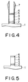
- Fig. 4 is a cross sectional view showing a structure after removing masking resist by ashing followed by cleaning with a organic solvent after dryetching in Example 1.
- Fig. 5 is a cross sectional view showing a structure after cleaning the semiconductor device shown in Fig. 4 by using the cleaning agent for the semiconductor device according to the present invention in Example 1.
- Fig. 6 is a cross sectional view showing a structure of a semiconductor device immediately after forming the conductive layer in Example 4.
- Fig. 7 is a cross sectional view showing a structure upon completing up as far as the mask forming step in Example 4.
- Fig. 8 is a cross sectional view showing a structure after removing a region of a conductive layer in Example 4 not covered with a photo-mask (non-masked region) by means of dryetching.
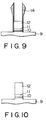
- Fig. 9 is a cross sectional view showing a structure after removing a masking resist by ashing followed by cleaning with an organic solvent after dryetching in Example 4.
- Fig. 10 is a cross sectional view showing a structure after cleaning the semiconductor device shown in Fig. 9 by using the cleaning agent for the semiconductor device according to the present invention in Example 4.
- the quaternary ammonium salt used in the present invention is represented by the following formula: [(R1)3N-R]+ ⁇ X ⁇ in which R represents an alkyl group of 1 to 4 carbon atoms or a hydroxyl substituted alkyl group of 1 to 4 carbon atoms, R1 represents an alkyl group of 1 to 4 carbon atoms and X represents an organic or inorganic acid group.
- Examples of the quaternary ammonium salt represented by the foregoing general formula include tetramethylammonium formate, tetramethylammonium acetate, tetramethylammonium propionate, tetramethylammonium butyrate, tetramethylammonium oxalate, tetramethylammonium malonate, tetramethylammonium maleate, tetramethylammonium fumarate, tetramethylammonium citraconate, tetramethylammonium benzoate, tetramethylammonium toluate, tetramethylammonium phthalate, tetramethylammonium acrylate, trimethyl(2-hydroxyethyl)ammonium formate, trimethyl(2-hydroxyethyl)ammonium acetate, trimethyl(2-hydroxyethyl)ammonium benzoate, trimethyl(2-hydroxyethyl)ammonium phthalate, tetraethylammonium
- the concentration of the quaternary ammonium salt in the cleaning agent for the semiconductor device according to the present invention is within a range from 1 to 60%, preferably, 10 to 50% by weight. If the concentration of the quaternary ammonium salt is less than 1% by weight, violent corrosion undesirably occurs to the wiring material, whereas if it is more than 60% by weight, the removing rate for the side wall protecting deposition film is unfavorably lowered.
- fluoro-compound in the cleaning agent for the semiconductor device there are mentioned, for example, hydrofluoric acid, ammonium fluoride, ammonium hydrogen fluoride, ammonium borofluoride, tetramethylammonium fluoride and tetramethylammonium hydrogen fluoride.
- the concentration of the fluoro-compound is from 0.1 to 10, preferably, 0.5 to 5% by weight. If the concentration of the fluoro-compound is less than 0.1% by weight, the removing rate for the side wall protecting deposition film is lowered, whereas violent corrosion occurs to the wiring material at a concentration higher than 10% by weight.
- an amide such as dimethylformamide, dimethylacetamide, formamide and N-methylpyrrolidone
- a lactone such as ⁇ -butyrolactone
- a nitrile such as acetonitrile and benzonitrile
- an alcohol such as methanol, ethanol, isopropanol and ethylene glycol
- an ester such as methyl acetate, ethyl acetate and methyl benzoate.
- the concentration of the organic solvent is from 1 to 60%, preferably, 20 to 55% by weight. If the concentration of the organic solvent is less than 1% by weight, violent corrosion occurs to the wiring material, whereas the removing rate for the side wall protecting deposition film is lowered at a concentration higher than 60% by weight.
- the temperature of the cleaning agent for the semiconductor device according to the present invention upon removing the side wall protecting deposition film is usually ordinary temperature, for example, 18 to 25°C. If the removing rate for the side wall protecting deposition film is remarkably low, it is used being heated, for example, to 25 to 60°C. Further, the cleaning temperature and the cleaning time are properly selected considering the state of the side wall protecting deposition film and the kind of the wiring materials.
- the peeling step is put into practice by applying the cleaning agent according to the present invention to a conventional method in which the semiconductor substrate to be processed is subjected, for example, to dipping cleaning by batch-wise system or to spray cleaning for each substrate, followed by cleaning with purified water and drying to complete the objective peeling process.
- the cleaning agent for the semiconductor device according to the present invention is used in the process for manufacturing the semiconductor device for the purpose of removing a protecting deposition film formed on the side walls of the conductive layer and the photoresist when a wiring structure by dryetching is formed after forming a mask with the photoresist for the conductive layer formed on the semiconductor substrate with a positive or negative type single-layer photoresist or a multilayer photoresist. Since the protecting deposition film can be peeled highly reliably by using the above-mentioned cleaning agent, the surface of the conductive layer is decontaminated and cleaned, so that no corrosion occurs.
- the cleaning agent for the semiconductor device according to the present invention is applicable also to the removal of the protecting deposition film formed upon dryetching of a titanium or tungsten layer which has heretofore been difficult to remove and thus making itself effectively usable in the manufacture of a semiconductor device or highly integrated circuit of a multilayer structure.
- a TiW layer 2 as a first metal film layer
- a CVD-W layer 3 as a second metal film layer
- an Al-Si-Cu layer 4 as a third metal film layer
- a TiN layer 5 as anti-reflection film
- a PLASMA TEOS layer 6 as a chemical resistant protecting film.
- Each of the metal films has a thickness of 600 ⁇ for the first metal film layer 2, 500 ⁇ for the second metal film layer 3, 5000 ⁇ for the third metal film layer, 200 ⁇ for the TiN layer 5 as the upper film layer and 400 ⁇ for the PLASMA TEOS film 6.
- the Al-Si-Cu layer 4 contained 1% by wt% of Si and 0.5% by weight of Cu.
- Fig. 2 shows a structure upon completion up as far as a mask forming process.
- a positive type photoresist 7 was applied to the conductive layer shown in Fig. 1 and then exposed to form a resist mask portion.
- the photoresist 7 used therein had a multilayer resist composed mainly of a novolac resin.
- Fig. 3 shows a structure after removing a region of the conductive layer not covered with the photo-mask (nonmasked region) by means of dryetching using a chloro-gas. Formation of the side wall protecting deposition film 8 was already observed on the side of the patterned conductive layer.
- Fig. 4 shows a structure after removing the masking resist by ashing followed by cleaning with an organic solvent after dryetching. It was confirmed that removal of the side wall protecting deposition film 8 was difficult by this method.
- Fig. 5 shows the structure after cleaning the semiconductor device shown in Fig. 4 by using a cleaning agent for the semiconductor device according to the present invention.
- a solution of ammonium fluoride/tetramethylammonium formate/dimethylformamide/water at 1/10/40/49(wt% ratio) was used as the cleaning agent for the semiconductor device and cleaning was carried out at 23°C for 20 min, followed by water washing.
- the same semiconductor device as that in Fig. 4 for Example 1 was cleaned by using a cleaning solution having a composition consisting of ammonium fluoride/tetramethylammonium formate/water at 2/45/53 (wt% ratio) at 23°C for 20 min and then washed wtih water.
- a cleaning solution having a composition consisting of ammonium fluoride/tetramethylammonium formate/water at 2/45/53 (wt% ratio) at 23°C for 20 min and then washed wtih water.
- the same semiconductor device as that in Fig. 4 for Example 1 was cleaned by using a cleaning solution having a composition consisting of tetramethylammonium fluoride/tetramethylammonium acetate/dimethylacetoamide/water at 5/15/40/40 (wt% ratio) at 25°C for 30 min and then washed with water.
- a cleaning solution having a composition consisting of tetramethylammonium fluoride/tetramethylammonium acetate/dimethylacetoamide/water at 5/15/40/40 (wt% ratio) at 25°C for 30 min and then washed with water.
- the side wall protecting deposition film was completely removed in same manner as in Example 1, so that the surface of the patterned conductive layer was decontaminated and cleaned.
- a Ti layer 10 as a first metal film layer
- a TiN layer 11 as a second metal film layer
- a W (tungsten) layer 12 as a third metal film layer.
- the film thickness for each of the metal films was 300 to 500 ⁇ for the first metal film layer 10, 500 to 700 ⁇ for the second metal film layer 11 and 3000 ⁇ for the third metal film layer 12.
- Fig. 7 shows a structure upon completion up as far as mask forming step.
- a positive type photoresist 13 was applied to the conductive layer shown in Fig. 6 and then exposed to form a resist mask portion.
- the photoresist 13 used therein had a multilayer resist composed mainly of a novolac resin.
- Fig. 8 shows a structure after removing a region of the conductive layer not covered with the photo-mask (nonmasked region) by means of dryetching. Formation of the side wall protecting deposition film 14 was already observed on the side of the patterned conductive layer.
- Fig. 9 shows the structure after removing the masking resist by ashing, after dryetching. It was confirmed that although the removal was possible up as far as the resist but the removal of the side wall protecting deposition film 14 was difficult by this method.
- Fig. 10 shows a structure after cleaning the semiconductor device in Fig. 9 by using a cleaning agent for the semiconductor device according to the present invention.
- An aqueous solution of ammonium fluoride/tetramethylammonium formate/dimethylformamide/water at 1/10/40/49 (wt% ratio) was used as the cleaning agent for the semiconductor device and cleaning was carried out at 23°C for 20 min, followed by water washing and drying. It can be seen in Fig. 10 that the side wall protecting deposition film 14 is removed and the surface of the patterned conductive layer is decontaminated and cleaned.
- the same semiconductor device as that in Fig. 9 for Example 4 was cleaned by using a cleaning solution having a composition consisting of ammonium fluoride/tetramethylammonium formate/water at 2/45/53 (wt% ratio) at 23°C for 20 min and then washed with water.
- a cleaning solution having a composition consisting of ammonium fluoride/tetramethylammonium formate/water at 2/45/53 (wt% ratio) at 23°C for 20 min and then washed with water.
- the side wall protecting deposition film 14 was completely removed in same manner as in Example 4, so that the surface of the patterned conductive layer was decontaminated and cleaned.
- the same semiconductor device as that in Fig. 9 for Example 4 was cleaned by using a cleaning solution having a composition consisting of ammonium fluoride/trimethyl(2-hydroxyethyl)ammonium formate/dimethylformamide/water at 2/20/30/48 (wt% ratio) at 25°C for 20 min and then washed with water.
- a cleaning solution having a composition consisting of ammonium fluoride/trimethyl(2-hydroxyethyl)ammonium formate/dimethylformamide/water at 2/20/30/48 (wt% ratio) at 25°C for 20 min and then washed with water.
- the side wall protecting deposition film 14 was completely removed in same manner as in Example 4, so that the surface of the patterned conductive layer was decontaminated and cleaned.
- the same semiconductor device as that in Fig. 9 for Example 4 was cleaned by using a cleaning solution having a composition consisting of tetramethylammonium formate/dimethylformamide/water at 10/40/50 (wt% ratio) at 25°C for 30 min as the cleaning conditions, followed by water washing. As a result, the side wall protecting deposition film 14 could not be removed.
Landscapes
- Physics & Mathematics (AREA)
- General Physics & Mathematics (AREA)
- Cleaning Or Drying Semiconductors (AREA)
- Detergent Compositions (AREA)
- Weting (AREA)
Applications Claiming Priority (3)
| Application Number | Priority Date | Filing Date | Title |
|---|---|---|---|
| JP520/94 | 1994-01-07 | ||
| JP00052094A JP3264405B2 (ja) | 1994-01-07 | 1994-01-07 | 半導体装置洗浄剤および半導体装置の製造方法 |
| JP52094 | 1994-01-07 |
Publications (3)
| Publication Number | Publication Date |
|---|---|
| EP0662705A2 true EP0662705A2 (de) | 1995-07-12 |
| EP0662705A3 EP0662705A3 (de) | 1995-09-27 |
| EP0662705B1 EP0662705B1 (de) | 2000-08-23 |
Family
ID=11476052
Family Applications (1)
| Application Number | Title | Priority Date | Filing Date |
|---|---|---|---|
| EP94120888A Expired - Lifetime EP0662705B1 (de) | 1994-01-07 | 1994-12-29 | Reinigungsmittel für Halbleiter-Anordnung und Verfahren zur Herstellung einer Halbleiter-Anordnung |
Country Status (6)
| Country | Link |
|---|---|
| US (1) | US6462005B1 (de) |
| EP (1) | EP0662705B1 (de) |
| JP (1) | JP3264405B2 (de) |
| KR (1) | KR100352692B1 (de) |
| DE (1) | DE69425643T2 (de) |
| TW (1) | TW324028B (de) |
Cited By (24)
| Publication number | Priority date | Publication date | Assignee | Title |
|---|---|---|---|---|
| EP0773480A1 (de) * | 1995-11-13 | 1997-05-14 | Tokyo Ohka Kogyo Co., Ltd. | Photolack-Entschichtungslösung und Verfahren unter Verwendung derselben |
| EP0762488A3 (de) * | 1995-08-18 | 1997-09-10 | Samsung Electronics Co Ltd | Reinigungslösung für Halbleiteranordnung und Reinigungsmethode |
| WO1998022568A1 (en) * | 1996-11-22 | 1998-05-28 | Advanced Chemical Systems International, Inc. | Stripping formulation including catechol, hydroxylamine, non-alkanolamine, water for post plasma ashed wafer cleaning |
| EP0827188A3 (de) * | 1996-08-09 | 1998-08-19 | Mitsubishi Gas Chemical Company, Inc. | Reinigungsflüssigkeit für die Herstellung von Halbleiter-Anordnungen und Verfahren zur Herstellung von Halbleiter-Anordnungen unter Verwendung derselben |
| WO1999021221A1 (en) * | 1997-10-20 | 1999-04-29 | Micron Technology, Inc. | Methods of forming conductive components and conductive lines |
| US5968848A (en) * | 1996-12-27 | 1999-10-19 | Tokyo Ohka Kogyo Co., Ltd. | Process for treating a lithographic substrate and a rinse solution for the treatment |
| US6068000A (en) * | 1996-07-11 | 2000-05-30 | Tokyo Ohka Kogyo Co., Ltd. | Substrate treatment method |
| WO2000066697A1 (en) * | 1999-05-03 | 2000-11-09 | Ekc Technology, Inc. | Compositions for cleaning organic and plasma etched residues for semiconductor devices |
| US6231677B1 (en) | 1998-02-27 | 2001-05-15 | Kanto Kagaku Kabushiki Kaisha | Photoresist stripping liquid composition |
| EP1044251A4 (de) * | 1997-10-14 | 2002-03-20 | Advanced Tech Materials | Ammoniumborat enthaltende zusammensetzungen zur entfernung von rückständen von halbleitersubstraten |
| US6468951B1 (en) * | 1996-10-03 | 2002-10-22 | Micron Technology, Inc. | Cleaning composition containing tetraalkylammonium salt and use thereof in semiconductor fabrication |
| WO2003006599A1 (en) * | 2001-07-09 | 2003-01-23 | Mallinckrodt Baker Inc. | Microelectronic cleaning compositions containing ammonia-free fluoride salts |
| US6703319B1 (en) * | 1999-06-17 | 2004-03-09 | Micron Technology, Inc. | Compositions and methods for removing etch residue |
| US6787293B2 (en) | 2002-03-22 | 2004-09-07 | Kanto Kagaku Kabushiki Kaisha | Photoresist residue remover composition |
| WO2004113486A1 (en) * | 2003-06-18 | 2004-12-29 | Tokyo Ohka Kogyo Co., Ltd. | Cleaning composition, method of cleaning semiconductor substrate, and method of forming wiring on semiconductor substrate |
| EP1334408A4 (de) * | 2000-09-25 | 2004-12-29 | Air Prod & Chem | Fotoresist-entfernungs-/reinigungszusammensetzungen mit aromatischen säureinhibitoren |
| US6864044B2 (en) | 2001-12-04 | 2005-03-08 | Kanto Kagaku Kabushiki Kaisha | Photoresist residue removing liquid composition |
| US7252718B2 (en) | 2002-05-31 | 2007-08-07 | Ekc Technology, Inc. | Forming a passivating aluminum fluoride layer and removing same for use in semiconductor manufacture |
| US7273060B2 (en) | 2002-01-28 | 2007-09-25 | Ekc Technology, Inc. | Methods for chemically treating a substrate using foam technology |
| US7393819B2 (en) | 2002-07-08 | 2008-07-01 | Mallinckrodt Baker, Inc. | Ammonia-free alkaline microelectronic cleaning compositions with improved substrate compatibility |
| US7456140B2 (en) | 2000-07-10 | 2008-11-25 | Ekc Technology, Inc. | Compositions for cleaning organic and plasma etched residues for semiconductor devices |
| WO2008081416A3 (en) * | 2007-01-03 | 2008-11-27 | Az Electronic Materials Usa | Stripper for coating layer |
| US7998914B2 (en) | 2005-12-01 | 2011-08-16 | Mitsubishi Gas Chemical Company, Inc. | Cleaning solution for semiconductor device or display device, and cleaning method |
| US8105998B2 (en) | 2006-10-24 | 2012-01-31 | Kanto Kagaku Kabushiki Kaisha | Liquid composition for removing photoresist residue and polymer residue |
Families Citing this family (37)
| Publication number | Priority date | Publication date | Assignee | Title |
|---|---|---|---|---|
| US5911836A (en) * | 1996-02-05 | 1999-06-15 | Mitsubishi Gas Chemical Company, Inc. | Method of producing semiconductor device and rinse for cleaning semiconductor device |
| JPH10154712A (ja) * | 1996-11-25 | 1998-06-09 | Fujitsu Ltd | 半導体装置の製造方法 |
| KR19990011638A (ko) * | 1997-07-24 | 1999-02-18 | 윤종용 | 반도체장치의 제조에 이용되는 세정액 |
| US6083419A (en) * | 1997-07-28 | 2000-07-04 | Cabot Corporation | Polishing composition including an inhibitor of tungsten etching |
| KR100510446B1 (ko) * | 1998-01-07 | 2005-10-21 | 삼성전자주식회사 | 반도체 장치의 콘택홀 세정방법 |
| KR100415261B1 (ko) * | 1998-03-26 | 2004-03-26 | 이기원 | 전자표시장치및기판용세정및식각조성물 |
| TW467953B (en) | 1998-11-12 | 2001-12-11 | Mitsubishi Gas Chemical Co | New detergent and cleaning method of using it |
| JP4224652B2 (ja) | 1999-03-08 | 2009-02-18 | 三菱瓦斯化学株式会社 | レジスト剥離液およびそれを用いたレジストの剥離方法 |
| KR100310253B1 (ko) * | 1999-06-28 | 2001-11-01 | 박종섭 | 메탈식각 또는 비아식각 후 발생하는 폴리머의 세정 방법 |
| JP3410403B2 (ja) | 1999-09-10 | 2003-05-26 | 東京応化工業株式会社 | ホトレジスト用剥離液およびこれを用いたホトレジスト剥離方法 |
| US6451707B2 (en) | 1999-12-07 | 2002-09-17 | Matsushita Electronics Corporation | Method of removing reaction product due to plasma ashing of a resist pattern |
| EP1360077A4 (de) | 2000-07-10 | 2009-06-24 | Ekc Technology Inc | Zusammensetzung zur reinigung von halbleitern von organischen und resten der plasma-ätzung |
| KR100419924B1 (ko) * | 2001-05-02 | 2004-02-25 | 삼성전자주식회사 | 세정액 및 이를 사용한 반사방지막 성분의 세정 방법 |
| JP4532776B2 (ja) | 2001-05-07 | 2010-08-25 | パナソニック株式会社 | 基板洗浄方法及び電子デバイスの製造方法 |
| JP3403187B2 (ja) | 2001-08-03 | 2003-05-06 | 東京応化工業株式会社 | ホトレジスト用剥離液 |
| JP2003129089A (ja) * | 2001-10-24 | 2003-05-08 | Daikin Ind Ltd | 洗浄用組成物 |
| US6703301B2 (en) * | 2002-04-26 | 2004-03-09 | Macronix International Co., Ltd. | Method of preventing tungsten plugs from corrosion |
| KR100514167B1 (ko) * | 2002-06-24 | 2005-09-09 | 삼성전자주식회사 | 세정액 및 이를 사용한 세라믹 부품의 세정 방법 |
| JP4443864B2 (ja) | 2002-07-12 | 2010-03-31 | 株式会社ルネサステクノロジ | レジストまたはエッチング残さ物除去用洗浄液および半導体装置の製造方法 |
| KR100464858B1 (ko) | 2002-08-23 | 2005-01-05 | 삼성전자주식회사 | 유기 스트리핑 조성물 및 이를 사용한 산화물 식각 방법 |
| JP2004277576A (ja) * | 2003-03-17 | 2004-10-07 | Daikin Ind Ltd | エッチング用又は洗浄用の溶液の製造法 |
| US20040220066A1 (en) * | 2003-05-01 | 2004-11-04 | Rohm And Haas Electronic Materials, L.L.C. | Stripper |
| KR101117939B1 (ko) | 2003-10-28 | 2012-02-29 | 사켐,인코포레이티드 | 세척액 및 에칭제 및 이의 사용 방법 |
| US6946396B2 (en) | 2003-10-30 | 2005-09-20 | Nissan Chemical Indusries, Ltd. | Maleic acid and ethylene urea containing formulation for removing residue from semiconductor substrate and method for cleaning wafer |
| JP4776191B2 (ja) * | 2004-08-25 | 2011-09-21 | 関東化学株式会社 | フォトレジスト残渣及びポリマー残渣除去組成物、並びにそれを用いた残渣除去方法 |
| US7922823B2 (en) | 2005-01-27 | 2011-04-12 | Advanced Technology Materials, Inc. | Compositions for processing of semiconductor substrates |
| US7923423B2 (en) | 2005-01-27 | 2011-04-12 | Advanced Technology Materials, Inc. | Compositions for processing of semiconductor substrates |
| JP4988165B2 (ja) | 2005-03-11 | 2012-08-01 | 関東化学株式会社 | フォトレジスト剥離液組成物及びフォトレジストの剥離方法 |
| US20070099806A1 (en) * | 2005-10-28 | 2007-05-03 | Stewart Michael P | Composition and method for selectively removing native oxide from silicon-containing surfaces |
| JP4826235B2 (ja) | 2005-12-01 | 2011-11-30 | 三菱瓦斯化学株式会社 | 半導体表面処理剤 |
| US20070219105A1 (en) * | 2006-03-17 | 2007-09-20 | Georgia Tech Research Corporation | Ionic Additives to Solvent-Based Strippers |
| US8685909B2 (en) | 2006-09-21 | 2014-04-01 | Advanced Technology Materials, Inc. | Antioxidants for post-CMP cleaning formulations |
| JP4499751B2 (ja) | 2006-11-21 | 2010-07-07 | エア プロダクツ アンド ケミカルズ インコーポレイテッド | フォトレジスト、エッチ残留物及びbarcを除去するための配合物及び同配合物を含む方法 |
| US8021490B2 (en) * | 2007-01-04 | 2011-09-20 | Eastman Chemical Company | Substrate cleaning processes through the use of solvents and systems |
| WO2010048139A2 (en) | 2008-10-21 | 2010-04-29 | Advanced Technology Materials, Inc. | Copper cleaning and protection formulations |
| JP2012058273A (ja) | 2010-09-03 | 2012-03-22 | Kanto Chem Co Inc | フォトレジスト残渣およびポリマー残渣除去液組成物 |
| CN112310121A (zh) * | 2020-10-22 | 2021-02-02 | Tcl华星光电技术有限公司 | 阵列基板及其制备方法、显示面板 |
Family Cites Families (18)
| Publication number | Priority date | Publication date | Assignee | Title |
|---|---|---|---|---|
| US3553143A (en) * | 1967-01-18 | 1971-01-05 | Purex Corp | Ammonium hydroxide containing wax stripper |
| US3915882A (en) * | 1972-11-10 | 1975-10-28 | Procter & Gamble | Soap compositions |
| US4056531A (en) * | 1973-09-07 | 1977-11-01 | Ethyl Corporation | Polymonoolefin quaternary ammonium salts of triethylenediamine |
| US3973322A (en) * | 1974-05-13 | 1976-08-10 | Hollis Engineering, Inc. | Mass soldering system and method |
| GB1573206A (en) * | 1975-11-26 | 1980-08-20 | Tokyo Shibaura Electric Co | Method of trating surfaces of intermediate products obtained in the manufacture of semiconductor devices |
| US4215005A (en) * | 1978-01-30 | 1980-07-29 | Allied Chemical Corporation | Organic stripping compositions and method for using same |
| US4265772A (en) * | 1978-11-16 | 1981-05-05 | The Procter & Gamble Company | Antistatic, fabric-softening detergent additive |
| US4184970A (en) * | 1978-11-16 | 1980-01-22 | The Procter & Gamble Company | Antistatic, fabric-softening detergent additive |
| US4343677A (en) * | 1981-03-23 | 1982-08-10 | Bell Telephone Laboratories, Incorporated | Method for patterning films using reactive ion etching thereof |
| US4647480A (en) * | 1983-07-25 | 1987-03-03 | Amchem Products, Inc. | Use of additive in aqueous cure of autodeposited coatings |
| US4520084A (en) * | 1984-06-07 | 1985-05-28 | Standard Oil Company (Indiana) | Etched metal electrodes and their use in nonaqueous electrochemical cells |
| US4522658A (en) * | 1984-06-21 | 1985-06-11 | Halliburton Company | Method and composition for protecting metal surfaces from oxidative environments |
| US4744834A (en) * | 1986-04-30 | 1988-05-17 | Noor Haq | Photoresist stripper comprising a pyrrolidinone, a diethylene glycol ether, a polyglycol and a quaternary ammonium hydroxide |
| JPS63114128A (ja) * | 1986-10-31 | 1988-05-19 | Showa Denko Kk | 表面処理液 |
| US4906349A (en) * | 1988-10-12 | 1990-03-06 | Zircoa Incorporation | Process for the manufacture of a measuring probe for a measuring head to detect the oxygen activity of metal melts and a measuring probe manufactured by such a process |
| SE8903452D0 (sv) * | 1989-10-19 | 1989-10-19 | Lars Aake Hilmer Haakansson | Foerfarande foer betning av jaern och staalytor |
| JP2906590B2 (ja) * | 1990-06-14 | 1999-06-21 | 三菱瓦斯化学株式会社 | アルミニウム配線半導体基板の表面処理剤 |
| DE4101564A1 (de) * | 1991-01-21 | 1992-07-23 | Riedel De Haen Ag | Aetzloesung fuer nasschemische prozesse der halbleiterherstellung |
-
1994
- 1994-01-07 JP JP00052094A patent/JP3264405B2/ja not_active Expired - Fee Related
- 1994-12-29 EP EP94120888A patent/EP0662705B1/de not_active Expired - Lifetime
- 1994-12-29 DE DE69425643T patent/DE69425643T2/de not_active Expired - Fee Related
- 1994-12-30 TW TW083112380A patent/TW324028B/zh not_active IP Right Cessation
-
1995
- 1995-01-05 US US08/369,215 patent/US6462005B1/en not_active Expired - Lifetime
- 1995-01-06 KR KR1019950000138A patent/KR100352692B1/ko not_active Expired - Fee Related
Cited By (39)
| Publication number | Priority date | Publication date | Assignee | Title |
|---|---|---|---|---|
| EP0762488A3 (de) * | 1995-08-18 | 1997-09-10 | Samsung Electronics Co Ltd | Reinigungslösung für Halbleiteranordnung und Reinigungsmethode |
| US5876509A (en) * | 1995-08-18 | 1999-03-02 | Samsung Electronics Co., Ltd. | Cleaning solution for cleaning semiconductor device and cleaning method using the same |
| US5792274A (en) * | 1995-11-13 | 1998-08-11 | Tokyo Ohka Kogyo Co., Ltd. | Remover solution composition for resist and method for removing resist using the same |
| US5905063A (en) * | 1995-11-13 | 1999-05-18 | Tokyo Ohka Kogyo Co., Ltd. | Remover solution composition for resist and method for removing resist using the same |
| EP0773480A1 (de) * | 1995-11-13 | 1997-05-14 | Tokyo Ohka Kogyo Co., Ltd. | Photolack-Entschichtungslösung und Verfahren unter Verwendung derselben |
| US6068000A (en) * | 1996-07-11 | 2000-05-30 | Tokyo Ohka Kogyo Co., Ltd. | Substrate treatment method |
| EP0827188A3 (de) * | 1996-08-09 | 1998-08-19 | Mitsubishi Gas Chemical Company, Inc. | Reinigungsflüssigkeit für die Herstellung von Halbleiter-Anordnungen und Verfahren zur Herstellung von Halbleiter-Anordnungen unter Verwendung derselben |
| KR100450559B1 (ko) * | 1996-08-09 | 2005-01-13 | 미츠비시 가스 가가쿠 가부시키가이샤 | 반도체소자제조용세정액및그것을사용한반도체소자의제조방법 |
| US5972862A (en) * | 1996-08-09 | 1999-10-26 | Mitsubishi Gas Chemical | Cleaning liquid for semiconductor devices |
| US6468951B1 (en) * | 1996-10-03 | 2002-10-22 | Micron Technology, Inc. | Cleaning composition containing tetraalkylammonium salt and use thereof in semiconductor fabrication |
| WO1998022568A1 (en) * | 1996-11-22 | 1998-05-28 | Advanced Chemical Systems International, Inc. | Stripping formulation including catechol, hydroxylamine, non-alkanolamine, water for post plasma ashed wafer cleaning |
| US5968848A (en) * | 1996-12-27 | 1999-10-19 | Tokyo Ohka Kogyo Co., Ltd. | Process for treating a lithographic substrate and a rinse solution for the treatment |
| EP1044251A4 (de) * | 1997-10-14 | 2002-03-20 | Advanced Tech Materials | Ammoniumborat enthaltende zusammensetzungen zur entfernung von rückständen von halbleitersubstraten |
| US6051502A (en) * | 1997-10-20 | 2000-04-18 | Micron Technology, Inc. | Methods of forming conductive components and methods of forming conductive lines |
| WO1999021221A1 (en) * | 1997-10-20 | 1999-04-29 | Micron Technology, Inc. | Methods of forming conductive components and conductive lines |
| US6231677B1 (en) | 1998-02-27 | 2001-05-15 | Kanto Kagaku Kabushiki Kaisha | Photoresist stripping liquid composition |
| WO2000066697A1 (en) * | 1999-05-03 | 2000-11-09 | Ekc Technology, Inc. | Compositions for cleaning organic and plasma etched residues for semiconductor devices |
| US6248704B1 (en) | 1999-05-03 | 2001-06-19 | Ekc Technology, Inc. | Compositions for cleaning organic and plasma etched residues for semiconductors devices |
| US6703319B1 (en) * | 1999-06-17 | 2004-03-09 | Micron Technology, Inc. | Compositions and methods for removing etch residue |
| US7456140B2 (en) | 2000-07-10 | 2008-11-25 | Ekc Technology, Inc. | Compositions for cleaning organic and plasma etched residues for semiconductor devices |
| KR100793590B1 (ko) | 2000-09-25 | 2008-01-14 | 에어 프로덕츠 앤드 케미칼스, 인코오포레이티드 | 방향족 산 억제제를 포함하는 포토레지스트스트리핑/클리닝 조성물 |
| EP1334408A4 (de) * | 2000-09-25 | 2004-12-29 | Air Prod & Chem | Fotoresist-entfernungs-/reinigungszusammensetzungen mit aromatischen säureinhibitoren |
| US7718591B2 (en) | 2001-07-09 | 2010-05-18 | Mallinckrodt Baker, Inc. | Microelectronic cleaning compositions containing ammonia-free fluoride salts for selective photoresist stripping and plasma ash residue cleaning |
| US7247208B2 (en) | 2001-07-09 | 2007-07-24 | Mallinckrodt Baker, Inc. | Microelectronic cleaning compositions containing ammonia-free fluoride salts |
| WO2003006599A1 (en) * | 2001-07-09 | 2003-01-23 | Mallinckrodt Baker Inc. | Microelectronic cleaning compositions containing ammonia-free fluoride salts |
| CN100513545C (zh) * | 2001-07-09 | 2009-07-15 | 马林克罗特贝克公司 | 包含无氨氟化物盐的微电子清洗组合物 |
| US6864044B2 (en) | 2001-12-04 | 2005-03-08 | Kanto Kagaku Kabushiki Kaisha | Photoresist residue removing liquid composition |
| US7273060B2 (en) | 2002-01-28 | 2007-09-25 | Ekc Technology, Inc. | Methods for chemically treating a substrate using foam technology |
| US6787293B2 (en) | 2002-03-22 | 2004-09-07 | Kanto Kagaku Kabushiki Kaisha | Photoresist residue remover composition |
| US7252718B2 (en) | 2002-05-31 | 2007-08-07 | Ekc Technology, Inc. | Forming a passivating aluminum fluoride layer and removing same for use in semiconductor manufacture |
| US7393819B2 (en) | 2002-07-08 | 2008-07-01 | Mallinckrodt Baker, Inc. | Ammonia-free alkaline microelectronic cleaning compositions with improved substrate compatibility |
| WO2004113486A1 (en) * | 2003-06-18 | 2004-12-29 | Tokyo Ohka Kogyo Co., Ltd. | Cleaning composition, method of cleaning semiconductor substrate, and method of forming wiring on semiconductor substrate |
| US7442675B2 (en) | 2003-06-18 | 2008-10-28 | Tokyo Ohka Kogyo Co., Ltd. | Cleaning composition and method of cleaning semiconductor substrate |
| KR100748903B1 (ko) * | 2003-06-18 | 2007-08-13 | 도오꾜오까고오교 가부시끼가이샤 | 세정제, 반도체 기판 세정 방법 및 반도체 기판에의 회로형성 방법 |
| US7998914B2 (en) | 2005-12-01 | 2011-08-16 | Mitsubishi Gas Chemical Company, Inc. | Cleaning solution for semiconductor device or display device, and cleaning method |
| US8105998B2 (en) | 2006-10-24 | 2012-01-31 | Kanto Kagaku Kabushiki Kaisha | Liquid composition for removing photoresist residue and polymer residue |
| WO2008081416A3 (en) * | 2007-01-03 | 2008-11-27 | Az Electronic Materials Usa | Stripper for coating layer |
| US8026201B2 (en) | 2007-01-03 | 2011-09-27 | Az Electronic Materials Usa Corp. | Stripper for coating layer |
| TWI494709B (zh) * | 2007-01-03 | 2015-08-01 | 馬克專利公司 | 用於塗層之剝離劑 |
Also Published As
| Publication number | Publication date |
|---|---|
| JPH07201794A (ja) | 1995-08-04 |
| DE69425643D1 (de) | 2000-09-28 |
| US6462005B1 (en) | 2002-10-08 |
| EP0662705B1 (de) | 2000-08-23 |
| JP3264405B2 (ja) | 2002-03-11 |
| KR100352692B1 (ko) | 2003-02-19 |
| EP0662705A3 (de) | 1995-09-27 |
| TW324028B (en) | 1998-01-01 |
| KR950034558A (ko) | 1995-12-28 |
| DE69425643T2 (de) | 2001-02-08 |
Similar Documents
| Publication | Publication Date | Title |
|---|---|---|
| EP0662705A2 (de) | Reinigungsmittel für Halbleiter-Anordnung und Verfahren zur Herstellung einer Halbleiter-Anordnung | |
| KR100242144B1 (ko) | 반도체 기판으로부터의 드라이 에칭 및 포토레지스트 잔류물 제거용 박리액, 및 이 박리액을 사용하는 배선 패턴의 형성방법 | |
| CN100526450C (zh) | 洗涤液及使用其的洗涤方法 | |
| EP0827188B1 (de) | Reinigungsflüssigkeit für die Herstellung von Halbleiter-Anordnungen und Verfahren zur Herstellung von Halbleiter-Anordnungen unter Verwendung derselben | |
| US5911836A (en) | Method of producing semiconductor device and rinse for cleaning semiconductor device | |
| US6454957B1 (en) | Ruthenium and ruthenium dioxide removal method and material | |
| US5476816A (en) | Process for etching an insulating layer after a metal etching step | |
| US20020068685A1 (en) | Post plasma ashing wafer cleaning formulation | |
| US6323168B1 (en) | Post plasma ashing wafer cleaning formulation | |
| JPH0728254A (ja) | レジスト用剥離液 | |
| KR19990023681A (ko) | 반도체장치용 세정제 | |
| JPH05259066A (ja) | ポジ型フォトレジスト用剥離液および半導体装置の製造方法 | |
| JP3236225B2 (ja) | 半導体装置及びその製造方法 | |
| US5882425A (en) | Composition and method for passivation of a metallization layer of a semiconductor circuit after metallization etching | |
| JP2002289569A (ja) | 残渣剥離剤組成物およびその使用方法 | |
| JP3968535B2 (ja) | 半導体素子の製造方法 | |
| JP4296320B2 (ja) | レジスト剥離剤組成物及びその使用方法 | |
| JP2000181083A (ja) | レジスト剥離剤組成物及びその使用方法 | |
| JPH11271985A (ja) | レジスト剥離剤組成物及びその使用方法 | |
| JPH11340183A (ja) | 半導体装置用洗浄液およびそれを用いた半導体装置の製 造方法 | |
| JPH0962013A (ja) | 半導体装置用洗浄剤及び半導体装置の製造方法 | |
| JPH09330981A (ja) | 半導体装置の製造方法 | |
| JP4223621B2 (ja) | レジスト剥離剤組成物の使用方法 | |
| JP5407121B2 (ja) | 洗浄剤組成物 | |
| JP2002164324A (ja) | 半導体装置の製造方法 |
Legal Events
| Date | Code | Title | Description |
|---|---|---|---|
| PUAI | Public reference made under article 153(3) epc to a published international application that has entered the european phase |
Free format text: ORIGINAL CODE: 0009012 |
|
| AK | Designated contracting states |
Kind code of ref document: A2 Designated state(s): DE FR GB IT NL |
|
| PUAL | Search report despatched |
Free format text: ORIGINAL CODE: 0009013 |
|
| AK | Designated contracting states |
Kind code of ref document: A3 Designated state(s): DE FR GB IT NL |
|
| 17P | Request for examination filed |
Effective date: 19960227 |
|
| 17Q | First examination report despatched |
Effective date: 19960403 |
|
| GRAG | Despatch of communication of intention to grant |
Free format text: ORIGINAL CODE: EPIDOS AGRA |
|
| GRAG | Despatch of communication of intention to grant |
Free format text: ORIGINAL CODE: EPIDOS AGRA |
|
| GRAH | Despatch of communication of intention to grant a patent |
Free format text: ORIGINAL CODE: EPIDOS IGRA |
|
| GRAH | Despatch of communication of intention to grant a patent |
Free format text: ORIGINAL CODE: EPIDOS IGRA |
|
| GRAA | (expected) grant |
Free format text: ORIGINAL CODE: 0009210 |
|
| AK | Designated contracting states |
Kind code of ref document: B1 Designated state(s): DE FR GB IT NL |
|
| REF | Corresponds to: |
Ref document number: 69425643 Country of ref document: DE Date of ref document: 20000928 |
|
| ET | Fr: translation filed | ||
| ITF | It: translation for a ep patent filed | ||
| PLBE | No opposition filed within time limit |
Free format text: ORIGINAL CODE: 0009261 |
|
| STAA | Information on the status of an ep patent application or granted ep patent |
Free format text: STATUS: NO OPPOSITION FILED WITHIN TIME LIMIT |
|
| 26N | No opposition filed | ||
| REG | Reference to a national code |
Ref country code: GB Ref legal event code: IF02 |
|
| PGFP | Annual fee paid to national office [announced via postgrant information from national office to epo] |
Ref country code: FR Payment date: 20021210 Year of fee payment: 9 |
|
| PGFP | Annual fee paid to national office [announced via postgrant information from national office to epo] |
Ref country code: NL Payment date: 20031205 Year of fee payment: 10 |
|
| PGFP | Annual fee paid to national office [announced via postgrant information from national office to epo] |
Ref country code: GB Payment date: 20031224 Year of fee payment: 10 |
|
| PGFP | Annual fee paid to national office [announced via postgrant information from national office to epo] |
Ref country code: DE Payment date: 20040108 Year of fee payment: 10 |
|
| PG25 | Lapsed in a contracting state [announced via postgrant information from national office to epo] |
Ref country code: FR Free format text: LAPSE BECAUSE OF NON-PAYMENT OF DUE FEES Effective date: 20040831 |
|
| REG | Reference to a national code |
Ref country code: FR Ref legal event code: ST |
|
| PG25 | Lapsed in a contracting state [announced via postgrant information from national office to epo] |
Ref country code: GB Free format text: LAPSE BECAUSE OF NON-PAYMENT OF DUE FEES Effective date: 20041229 |
|
| PG25 | Lapsed in a contracting state [announced via postgrant information from national office to epo] |
Ref country code: NL Free format text: LAPSE BECAUSE OF NON-PAYMENT OF DUE FEES Effective date: 20050701 Ref country code: DE Free format text: LAPSE BECAUSE OF NON-PAYMENT OF DUE FEES Effective date: 20050701 |
|
| GBPC | Gb: european patent ceased through non-payment of renewal fee |
Effective date: 20041229 |
|
| NLV4 | Nl: lapsed or anulled due to non-payment of the annual fee |
Effective date: 20050701 |
|
| PG25 | Lapsed in a contracting state [announced via postgrant information from national office to epo] |
Ref country code: IT Free format text: LAPSE BECAUSE OF NON-PAYMENT OF DUE FEES;WARNING: LAPSES OF ITALIAN PATENTS WITH EFFECTIVE DATE BEFORE 2007 MAY HAVE OCCURRED AT ANY TIME BEFORE 2007. THE CORRECT EFFECTIVE DATE MAY BE DIFFERENT FROM THE ONE RECORDED. Effective date: 20051229 |