EP0663690A2 - Veraschungsverfahren zum Entfernen einer organischen Schicht auf einer Halbleiteranordnung während ihrer Herstellung - Google Patents
Veraschungsverfahren zum Entfernen einer organischen Schicht auf einer Halbleiteranordnung während ihrer Herstellung Download PDFInfo
- Publication number
- EP0663690A2 EP0663690A2 EP95103878A EP95103878A EP0663690A2 EP 0663690 A2 EP0663690 A2 EP 0663690A2 EP 95103878 A EP95103878 A EP 95103878A EP 95103878 A EP95103878 A EP 95103878A EP 0663690 A2 EP0663690 A2 EP 0663690A2
- Authority
- EP
- European Patent Office
- Prior art keywords
- gas
- ashing
- reactant gas
- oxygen
- nitrogen
- Prior art date
- Legal status (The legal status is an assumption and is not a legal conclusion. Google has not performed a legal analysis and makes no representation as to the accuracy of the status listed.)
- Granted
Links
Images


Classifications
-
- H—ELECTRICITY
- H10—SEMICONDUCTOR DEVICES; ELECTRIC SOLID-STATE DEVICES NOT OTHERWISE PROVIDED FOR
- H10P—GENERIC PROCESSES OR APPARATUS FOR THE MANUFACTURE OR TREATMENT OF DEVICES COVERED BY CLASS H10
- H10P50/00—Etching of wafers, substrates or parts of devices
- H10P50/20—Dry etching; Plasma etching; Reactive-ion etching
- H10P50/28—Dry etching; Plasma etching; Reactive-ion etching of insulating materials
- H10P50/286—Dry etching; Plasma etching; Reactive-ion etching of insulating materials of organic materials
- H10P50/287—Dry etching; Plasma etching; Reactive-ion etching of insulating materials of organic materials by chemical means
-
- G—PHYSICS
- G03—PHOTOGRAPHY; CINEMATOGRAPHY; ANALOGOUS TECHNIQUES USING WAVES OTHER THAN OPTICAL WAVES; ELECTROGRAPHY; HOLOGRAPHY
- G03F—PHOTOMECHANICAL PRODUCTION OF TEXTURED OR PATTERNED SURFACES, e.g. FOR PRINTING, FOR PROCESSING OF SEMICONDUCTOR DEVICES; MATERIALS THEREFOR; ORIGINALS THEREFOR; APPARATUS SPECIALLY ADAPTED THEREFOR
- G03F7/00—Photomechanical, e.g. photolithographic, production of textured or patterned surfaces, e.g. printing surfaces; Materials therefor, e.g. comprising photoresists; Apparatus specially adapted therefor
- G03F7/26—Processing photosensitive materials; Apparatus therefor
- G03F7/42—Stripping or agents therefor
- G03F7/427—Stripping or agents therefor using plasma means only
Definitions
- the property of the resist is changed during the process of ion implantation and dry etching, which are widely performed in the fabricating process of the LSI or the VLSI, so that a long time is required for performing ashing, in other words, the ashing rate of the resist becomes small. Since the resist is used many times in the fabrication process of the LSI or the VLSI, the ashing rate for each resist should be large to improve the throughput of the fabrication of the LSI or the VLSI.
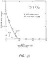
- Fig. 7 is a schematical drawing of a vacuum chamber of a down-flow ashing apparatus.
- the flow rate of each component gas is set 720 SCCM, 100 SCCM and 180 SCCM for O2, H2O and N2, respectively, as a desirable example.
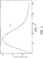
- flow rate of N2 is not limited if the flow ratio of N2 to the mixed gas of O2 and N2 is larger than 5%, because the ashing rate is constant regardless of the flow ratio when the flow ratio exceeds 5% as seen in Fig. 9.
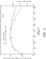
- the flow rate of H2O is not limited if the flow ratio of H2O to the mixed gas of O2 and H2O is larger than 1%, because the activation energy is about 0.4 eV regardless of the flow ratio when the flow ratio exceeds 1%, as seen in Fig. 6.
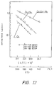
- the ashing rate is shown by a line connecting white squares in Fig. 12 represented in Arrhenius plot, and the activation energy is shown with the flow rate of H2 to the reactant gas composed of O2, H2 and N2 in Fig. 13.
Landscapes
- Physics & Mathematics (AREA)
- Engineering & Computer Science (AREA)
- Plasma & Fusion (AREA)
- General Physics & Mathematics (AREA)
- Drying Of Semiconductors (AREA)
- Exposure Of Semiconductors, Excluding Electron Or Ion Beam Exposure (AREA)
Applications Claiming Priority (4)
| Application Number | Priority Date | Filing Date | Title |
|---|---|---|---|
| JP142673/88 | 1988-06-09 | ||
| JP14267388 | 1988-06-09 | ||
| JP14267388 | 1988-06-09 | ||
| EP89110295A EP0345757B1 (de) | 1988-06-09 | 1989-06-07 | Veraschungsverfahren zum Entfernen einer organischen Schicht auf einer Halbleiteranordnung während ihrer Herstellung |
Related Parent Applications (2)
| Application Number | Title | Priority Date | Filing Date |
|---|---|---|---|
| EP89110295.6 Division | 1989-06-07 | ||
| EP89110295A Division EP0345757B1 (de) | 1988-06-09 | 1989-06-07 | Veraschungsverfahren zum Entfernen einer organischen Schicht auf einer Halbleiteranordnung während ihrer Herstellung |
Publications (3)
| Publication Number | Publication Date |
|---|---|
| EP0663690A2 true EP0663690A2 (de) | 1995-07-19 |
| EP0663690A3 EP0663690A3 (de) | 1998-03-11 |
| EP0663690B1 EP0663690B1 (de) | 2003-12-03 |
Family
ID=15320846
Family Applications (2)
| Application Number | Title | Priority Date | Filing Date |
|---|---|---|---|
| EP89110295A Expired - Lifetime EP0345757B1 (de) | 1988-06-09 | 1989-06-07 | Veraschungsverfahren zum Entfernen einer organischen Schicht auf einer Halbleiteranordnung während ihrer Herstellung |
| EP95103878A Expired - Lifetime EP0663690B1 (de) | 1988-06-09 | 1989-06-07 | Veraschungsverfahren zum Entfernen einer organischen Schicht auf einer Halbleiteranordnung während ihrer Herstellung |
Family Applications Before (1)
| Application Number | Title | Priority Date | Filing Date |
|---|---|---|---|
| EP89110295A Expired - Lifetime EP0345757B1 (de) | 1988-06-09 | 1989-06-07 | Veraschungsverfahren zum Entfernen einer organischen Schicht auf einer Halbleiteranordnung während ihrer Herstellung |
Country Status (5)
| Country | Link |
|---|---|
| US (2) | US4961820A (de) |
| EP (2) | EP0345757B1 (de) |
| JP (1) | JPH0777214B2 (de) |
| KR (1) | KR930002679B1 (de) |
| DE (2) | DE68928291T2 (de) |
Cited By (6)
| Publication number | Priority date | Publication date | Assignee | Title |
|---|---|---|---|---|
| EP0868836A4 (de) * | 1996-09-24 | 2002-02-13 | Fusion Systems Corp | Durch fluor unterstutztes abziehverfahren und ruckstandbeseitung in stromabwarts plasmaverascher aus saphir |
| US6440864B1 (en) | 2000-06-30 | 2002-08-27 | Applied Materials Inc. | Substrate cleaning process |
| EP0820641B1 (de) * | 1995-04-13 | 2002-11-27 | North Carolina State University | Verfahren für verbesserte wasserdampf-ladungsteilchenstrahlbearbeitung |
| EP1143498A3 (de) * | 2000-04-02 | 2003-10-22 | Axcelis Technologies, Inc. | Verfahren zur Entfernung von Photolack und Rückständen nach einer Ätzung |
| US6692903B2 (en) | 2000-12-13 | 2004-02-17 | Applied Materials, Inc | Substrate cleaning apparatus and method |
| US7214473B2 (en) | 2002-01-04 | 2007-05-08 | Nec Lcd Technologies Ltd. | Method for removing patterned layer from lower layer through reflow |
Families Citing this family (87)
| Publication number | Priority date | Publication date | Assignee | Title |
|---|---|---|---|---|
| JPH0777211B2 (ja) * | 1987-08-19 | 1995-08-16 | 富士通株式会社 | アッシング方法 |
| JP2890432B2 (ja) * | 1989-01-10 | 1999-05-17 | 富士通株式会社 | 有機物の灰化方法 |
| EP0416774B1 (de) * | 1989-08-28 | 2000-11-15 | Hitachi, Ltd. | Verfahren zur Behandlung eines Aluminium enthaltenden Musters |
| EP0463870B1 (de) * | 1990-06-26 | 1999-02-24 | Fujitsu Limited | Plasmabehandlungsverfahren eines Resists unter Verwendung von Wasserstoffgas |
| WO1992000601A1 (fr) * | 1990-06-27 | 1992-01-09 | Fujitsu Limited | Procede de fabrication d'un circuit integre a semi-conducteurs et appareil de fabrication correspondant |
| JP3013446B2 (ja) * | 1990-12-28 | 2000-02-28 | ソニー株式会社 | ドライエッチング方法 |
| JPH04314349A (ja) * | 1991-04-11 | 1992-11-05 | Mitsutoyo Corp | 真空リソグラフィ装置 |
| US5271800A (en) * | 1991-07-12 | 1993-12-21 | The United States Of America As Represented By The Administrator Of National Aeronautics And Space Administration | Method for anisotropic etching in the manufacture of semiconductor devices |
| US5174856A (en) * | 1991-08-26 | 1992-12-29 | Applied Materials, Inc. | Method for removal of photoresist over metal which also removes or inactivates corrosion-forming materials remaining from previous metal etch |
| JP3084910B2 (ja) * | 1992-03-18 | 2000-09-04 | ヤマハ株式会社 | 配線形成法 |
| JPH06188229A (ja) * | 1992-12-16 | 1994-07-08 | Tokyo Electron Yamanashi Kk | エッチングの後処理方法 |
| WO1995002472A1 (en) * | 1993-07-16 | 1995-01-26 | Fusion Systems Corporation | Post treatment of a coated substrate with a gas containing excited halogen to remove residues |
| US5418431A (en) * | 1993-08-27 | 1995-05-23 | Hughes Aircraft Company | RF plasma source and antenna therefor |
| US5382316A (en) * | 1993-10-29 | 1995-01-17 | Applied Materials, Inc. | Process for simultaneous removal of photoresist and polysilicon/polycide etch residues from an integrated circuit structure |
| JP2731730B2 (ja) * | 1993-12-22 | 1998-03-25 | インターナショナル・ビジネス・マシーンズ・コーポレイション | フォトレジストの除去方法 |
| WO1995021458A1 (en) * | 1994-02-03 | 1995-08-10 | Applied Materials, Inc. | Stripping, passivation and corrosion inhibition of semiconductor substrates |
| JPH07221075A (ja) * | 1994-02-03 | 1995-08-18 | Fujitsu Ltd | アッシング処理方法 |
| US5545289A (en) * | 1994-02-03 | 1996-08-13 | Applied Materials, Inc. | Passivating, stripping and corrosion inhibition of semiconductor substrates |
| JP3529849B2 (ja) * | 1994-05-23 | 2004-05-24 | 富士通株式会社 | 半導体装置の製造方法 |
| US5814134A (en) * | 1994-06-10 | 1998-09-29 | Johnson & Johnson Vision Products, Inc. | Apparatus and method for degassing deionized water for inspection and packaging |
| US5578331A (en) * | 1994-06-10 | 1996-11-26 | Vision Products, Inc. | Automated apparatus for preparing contact lenses for inspection and packaging |
| US5528878A (en) | 1994-06-10 | 1996-06-25 | Johnson & Johnson Vision Products, Inc. | Automated apparatus and method for consolidating products for packaging |
| US5850107A (en) * | 1994-06-10 | 1998-12-15 | Johnson & Johnson Vision Products, Inc. | Mold separation method and apparatus |
| US5811022A (en) | 1994-11-15 | 1998-09-22 | Mattson Technology, Inc. | Inductive plasma reactor |
| JPH08186098A (ja) * | 1994-12-27 | 1996-07-16 | Ryoden Semiconductor Syst Eng Kk | 感光性樹脂の除去方法および除去装置 |
| JPH08186099A (ja) * | 1994-12-29 | 1996-07-16 | Sharp Corp | レジストのアッシング方法 |
| US5900351A (en) * | 1995-01-17 | 1999-05-04 | International Business Machines Corporation | Method for stripping photoresist |
| US5674409A (en) * | 1995-03-16 | 1997-10-07 | International Business Machines Corporation | Nanolithographic method of forming fine lines |
| US6060397A (en) * | 1995-07-14 | 2000-05-09 | Applied Materials, Inc. | Gas chemistry for improved in-situ cleaning of residue for a CVD apparatus |
| US5567271A (en) * | 1995-07-26 | 1996-10-22 | Chartered Semiconductor Manufacturing Pte Ltd | Oxygen reactive ion etch (RIE) plasma method for removing oxidized organic residues from semiconductor substrates |
| US5705428A (en) * | 1995-08-03 | 1998-01-06 | Chartered Semiconductor Manufacturing Pte, Ltd. | Method for preventing titanium lifting during and after metal etching |
| TW371796B (en) * | 1995-09-08 | 1999-10-11 | Semiconductor Energy Lab Co Ltd | Method and apparatus for manufacturing a semiconductor device |
| US6228751B1 (en) * | 1995-09-08 | 2001-05-08 | Semiconductor Energy Laboratory Co., Ltd. | Method of manufacturing a semiconductor device |
| AU712870B2 (en) | 1995-09-29 | 1999-11-18 | Johnson & Johnson Vision Products, Inc. | Automated apparatus and method for consolidating products for packaging |
| US5824604A (en) * | 1996-01-23 | 1998-10-20 | Mattson Technology, Inc. | Hydrocarbon-enhanced dry stripping of photoresist |
| US6013574A (en) * | 1996-01-30 | 2000-01-11 | Advanced Micro Devices, Inc. | Method of forming low resistance contact structures in vias arranged between two levels of interconnect lines |
| KR100234532B1 (ko) * | 1996-09-21 | 1999-12-15 | 윤종용 | 반도체 제조공정의 포토레지스트 세정용 시너 조성물 및 그를 이용한 반도체장치의 제조방법 |
| US5795831A (en) * | 1996-10-16 | 1998-08-18 | Ulvac Technologies, Inc. | Cold processes for cleaning and stripping photoresist from surfaces of semiconductor wafers |
| US5811358A (en) * | 1997-01-03 | 1998-09-22 | Mosel Vitelic Inc. | Low temperature dry process for stripping photoresist after high dose ion implantation |
| US6379576B2 (en) | 1997-11-17 | 2002-04-30 | Mattson Technology, Inc. | Systems and methods for variable mode plasma enhanced processing of semiconductor wafers |
| JP3193335B2 (ja) * | 1997-12-12 | 2001-07-30 | 松下電器産業株式会社 | 半導体装置の製造方法 |
| US5970376A (en) * | 1997-12-29 | 1999-10-19 | Taiwan Semiconductor Manufacturing Company, Ltd. | Post via etch plasma treatment method for forming with attenuated lateral etching a residue free via through a silsesquioxane spin-on-glass (SOG) dielectric layer |
| US6231775B1 (en) | 1998-01-28 | 2001-05-15 | Anon, Inc. | Process for ashing organic materials from substrates |
| EP0940846A1 (de) * | 1998-03-06 | 1999-09-08 | Interuniversitair Micro-Elektronica Centrum Vzw | Verfahren zum Entschichten von implantierten Photolacken |
| US6105588A (en) | 1998-05-27 | 2000-08-22 | Micron Technology, Inc. | Method of resist stripping during semiconductor device fabrication |
| US6410417B1 (en) * | 1998-11-05 | 2002-06-25 | Promos Technologies, Inc. | Method of forming tungsten interconnect and vias without tungsten loss during wet stripping of photoresist polymer |
| DE19855924B4 (de) * | 1998-11-19 | 2006-02-16 | Mosel Vitelic Inc. | Herstellungsverfahren für eine Verbindung |
| US6372150B1 (en) * | 1998-12-18 | 2002-04-16 | Cypress Semiconductor Corp. | High vapor plasma strip methods and devices to enhance the reduction of organic residues over metal surfaces |
| US20040074525A1 (en) * | 2001-03-27 | 2004-04-22 | Widman Michael F. | Transfer apparatus and method and a transfer apparatus cleaner and method |
| FR2789804B1 (fr) * | 1999-02-17 | 2002-08-23 | France Telecom | Procede de gravure anisotrope par plasma gazeux d'un materiau polymere dielectrique organique et application a la microelectronique |
| US6494021B1 (en) | 1999-02-18 | 2002-12-17 | Johnson & Johnson Vision Care, Inc. | Contact lens transfer and material removal system |
| US6242350B1 (en) * | 1999-03-18 | 2001-06-05 | Taiwan Semiconductor Manufacturing Company | Post gate etch cleaning process for self-aligned gate mosfets |
| US6805139B1 (en) | 1999-10-20 | 2004-10-19 | Mattson Technology, Inc. | Systems and methods for photoresist strip and residue treatment in integrated circuit manufacturing |
| US20050022839A1 (en) * | 1999-10-20 | 2005-02-03 | Savas Stephen E. | Systems and methods for photoresist strip and residue treatment in integrated circuit manufacturing |
| US6431182B1 (en) | 1999-10-27 | 2002-08-13 | Advanced Micro Devices, Inc. | Plasma treatment for polymer removal after via etch |
| US6235440B1 (en) | 1999-11-12 | 2001-05-22 | Taiwan Semiconductor Manufacturing Company | Method to control gate CD |
| JP3509709B2 (ja) * | 2000-07-19 | 2004-03-22 | 株式会社村田製作所 | 圧電薄膜共振子及び圧電薄膜共振子の製造方法 |
| US6834656B2 (en) * | 2001-05-23 | 2004-12-28 | Axcelis Technology, Inc. | Plasma process for removing polymer and residues from substrates |
| US6774045B1 (en) * | 2001-07-11 | 2004-08-10 | Lam Research Corporation | Residual halogen reduction with microwave stripper |
| US6836692B2 (en) * | 2001-08-09 | 2004-12-28 | Johnson & Johnson Vision Care, Inc. | System and method for intelligent lens transfer |
| US6647994B1 (en) | 2002-01-02 | 2003-11-18 | Taiwan Semiconductor Manufacturing Company | Method of resist stripping over low-k dielectric material |
| JP2003282571A (ja) * | 2002-03-25 | 2003-10-03 | Toshiba Corp | 半導体装置の製造方法 |
| US6777173B2 (en) * | 2002-08-30 | 2004-08-17 | Lam Research Corporation | H2O vapor as a processing gas for crust, resist, and residue removal for post ion implant resist strip |
| US7232767B2 (en) * | 2003-04-01 | 2007-06-19 | Mattson Technology, Inc. | Slotted electrostatic shield modification for improved etch and CVD process uniformity |
| US7514012B2 (en) * | 2004-01-27 | 2009-04-07 | Texas Instruments Incorporated | Pre-oxidization of deformable elements of microstructures |
| US20110061679A1 (en) * | 2004-06-17 | 2011-03-17 | Uvtech Systems, Inc. | Photoreactive Removal of Ion Implanted Resist |
| US20070054492A1 (en) * | 2004-06-17 | 2007-03-08 | Elliott David J | Photoreactive removal of ion implanted resist |
| US20050279453A1 (en) | 2004-06-17 | 2005-12-22 | Uvtech Systems, Inc. | System and methods for surface cleaning |
| US20070186953A1 (en) * | 2004-07-12 | 2007-08-16 | Savas Stephen E | Systems and Methods for Photoresist Strip and Residue Treatment in Integrated Circuit Manufacturing |
| JP4588391B2 (ja) * | 2004-09-01 | 2010-12-01 | 芝浦メカトロニクス株式会社 | アッシング方法及びアッシング装置 |
| US8193096B2 (en) | 2004-12-13 | 2012-06-05 | Novellus Systems, Inc. | High dose implantation strip (HDIS) in H2 base chemistry |
| US8093070B2 (en) * | 2004-12-17 | 2012-01-10 | Texas Instruments Incorporated | Method for leakage reduction in fabrication of high-density FRAM arrays |
| KR100607777B1 (ko) * | 2004-12-27 | 2006-08-01 | 동부일렉트로닉스 주식회사 | 반도체 소자의 제조 방법 |
| US20070123049A1 (en) * | 2005-11-17 | 2007-05-31 | Kao-Su Huang | Semiconductor process and method for removing condensed gaseous etchant residues on wafer |
| KR20080023814A (ko) * | 2006-09-12 | 2008-03-17 | 주식회사 하이닉스반도체 | 반도체소자의 미세패턴 형성방법 |
| CN100576497C (zh) * | 2006-12-20 | 2009-12-30 | 中芯国际集成电路制造(上海)有限公司 | 形成集成电路器件自对准接触的方法 |
| US8435895B2 (en) | 2007-04-04 | 2013-05-07 | Novellus Systems, Inc. | Methods for stripping photoresist and/or cleaning metal regions |
| US20110143548A1 (en) | 2009-12-11 | 2011-06-16 | David Cheung | Ultra low silicon loss high dose implant strip |
| US9613825B2 (en) | 2011-08-26 | 2017-04-04 | Novellus Systems, Inc. | Photoresist strip processes for improved device integrity |
| CN102651370B (zh) * | 2012-01-04 | 2014-12-10 | 京东方科技集团股份有限公司 | 一种tft阵列基板、制造方法及显示装置 |
| CN104956476B (zh) * | 2013-11-06 | 2017-11-14 | 马特森技术有限公司 | 用于垂直nand器件的新型掩模去除方法策略 |
| US10050035B2 (en) | 2014-01-17 | 2018-08-14 | Taiwan Semiconductor Manufacturing Company, Ltd. | Method of making protective layer over polysilicon structure |
| JP2015216176A (ja) * | 2014-05-08 | 2015-12-03 | キヤノン株式会社 | 半導体装置の製造方法、及び、半導体装置 |
| US9514954B2 (en) | 2014-06-10 | 2016-12-06 | Lam Research Corporation | Peroxide-vapor treatment for enhancing photoresist-strip performance and modifying organic films |
| KR102713031B1 (ko) * | 2020-07-02 | 2024-10-07 | 창신 메모리 테크놀로지즈 아이엔씨 | 반도체 구조의 처리 방법 및 형성 방법 |
| CN113889405B (zh) | 2020-07-02 | 2024-07-05 | 长鑫存储技术有限公司 | 半导体结构的处理方法及形成方法 |
| CN114442443B (zh) * | 2020-10-30 | 2025-09-02 | 江苏鲁汶仪器股份有限公司 | 一种光刻胶剥离方法 |
Family Cites Families (12)
| Publication number | Priority date | Publication date | Assignee | Title |
|---|---|---|---|---|
| US3837856A (en) * | 1967-04-04 | 1974-09-24 | Signetics Corp | Method for removing photoresist in manufacture of semiconductor devices |
| JPS5751265A (en) * | 1980-09-10 | 1982-03-26 | Hitachi Ltd | Microwave plasma etching device |
| US4529860A (en) * | 1982-08-02 | 1985-07-16 | Motorola, Inc. | Plasma etching of organic materials |
| JPS59163826A (ja) * | 1983-03-08 | 1984-09-14 | Toshiba Corp | ドライエツチング方法 |
| US4501061A (en) * | 1983-05-31 | 1985-02-26 | Advanced Micro Devices, Inc. | Fluorine plasma oxidation of residual sulfur species |
| JPS6050923A (ja) * | 1983-08-31 | 1985-03-22 | Hitachi Ltd | プラズマ表面処理方法 |
| US4689112A (en) * | 1985-05-17 | 1987-08-25 | Emergent Technologies Corporation | Method and apparatus for dry processing of substrates |
| US4699689A (en) * | 1985-05-17 | 1987-10-13 | Emergent Technologies Corporation | Method and apparatus for dry processing of substrates |
| US4673456A (en) * | 1985-09-17 | 1987-06-16 | Machine Technology, Inc. | Microwave apparatus for generating plasma afterglows |
| JPH0777211B2 (ja) * | 1987-08-19 | 1995-08-16 | 富士通株式会社 | アッシング方法 |
| JPH01200628A (ja) * | 1988-02-05 | 1989-08-11 | Toshiba Corp | ドライエッチング方法 |
| EP0305946B1 (de) * | 1987-08-28 | 1996-10-30 | Kabushiki Kaisha Toshiba | Plasma-Entschichtungsverfahren für organische und anorganische Schichten |
-
1989
- 1989-06-05 US US07/361,178 patent/US4961820A/en not_active Expired - Lifetime
- 1989-06-07 DE DE68928291T patent/DE68928291T2/de not_active Expired - Fee Related
- 1989-06-07 EP EP89110295A patent/EP0345757B1/de not_active Expired - Lifetime
- 1989-06-07 EP EP95103878A patent/EP0663690B1/de not_active Expired - Lifetime
- 1989-06-07 DE DE68929503T patent/DE68929503T2/de not_active Expired - Fee Related
- 1989-06-09 KR KR1019890007964A patent/KR930002679B1/ko not_active Expired - Fee Related
- 1989-06-09 JP JP1147431A patent/JPH0777214B2/ja not_active Expired - Lifetime
-
1990
- 1990-05-18 US US07/524,934 patent/US5057187A/en not_active Expired - Lifetime
Cited By (6)
| Publication number | Priority date | Publication date | Assignee | Title |
|---|---|---|---|---|
| EP0820641B1 (de) * | 1995-04-13 | 2002-11-27 | North Carolina State University | Verfahren für verbesserte wasserdampf-ladungsteilchenstrahlbearbeitung |
| EP0868836A4 (de) * | 1996-09-24 | 2002-02-13 | Fusion Systems Corp | Durch fluor unterstutztes abziehverfahren und ruckstandbeseitung in stromabwarts plasmaverascher aus saphir |
| EP1143498A3 (de) * | 2000-04-02 | 2003-10-22 | Axcelis Technologies, Inc. | Verfahren zur Entfernung von Photolack und Rückständen nach einer Ätzung |
| US6440864B1 (en) | 2000-06-30 | 2002-08-27 | Applied Materials Inc. | Substrate cleaning process |
| US6692903B2 (en) | 2000-12-13 | 2004-02-17 | Applied Materials, Inc | Substrate cleaning apparatus and method |
| US7214473B2 (en) | 2002-01-04 | 2007-05-08 | Nec Lcd Technologies Ltd. | Method for removing patterned layer from lower layer through reflow |
Also Published As
| Publication number | Publication date |
|---|---|
| US5057187A (en) | 1991-10-15 |
| DE68929503T2 (de) | 2004-06-09 |
| DE68928291T2 (de) | 1998-04-02 |
| EP0663690A3 (de) | 1998-03-11 |
| EP0345757A2 (de) | 1989-12-13 |
| EP0345757A3 (de) | 1991-01-30 |
| DE68929503D1 (de) | 2004-01-15 |
| DE68928291D1 (de) | 1997-10-09 |
| JPH0777214B2 (ja) | 1995-08-16 |
| JPH0277125A (ja) | 1990-03-16 |
| KR930002679B1 (ko) | 1993-04-07 |
| KR910001909A (ko) | 1991-01-31 |
| EP0663690B1 (de) | 2003-12-03 |
| EP0345757B1 (de) | 1997-09-03 |
| US4961820A (en) | 1990-10-09 |
Similar Documents
| Publication | Publication Date | Title |
|---|---|---|
| EP0663690A2 (de) | Veraschungsverfahren zum Entfernen einer organischen Schicht auf einer Halbleiteranordnung während ihrer Herstellung | |
| US4676868A (en) | Method for planarizing semiconductor substrates | |
| US7153779B2 (en) | Method to eliminate striations and surface roughness caused by dry etch | |
| US6387819B1 (en) | Method for etching low K dielectric layers | |
| US7049244B2 (en) | Method for enhancing silicon dioxide to silicon nitride selectivity | |
| US4983254A (en) | Processing for stripping organic material | |
| US6951823B2 (en) | Plasma ashing process | |
| US4613400A (en) | In-situ photoresist capping process for plasma etching | |
| KR100388570B1 (ko) | 고 종횡비 개구를 형성하는 방법 | |
| EP0078161A2 (de) | Materialien und Verfahren zum Plasmaätzen von Oxyden und Nitriden von Silizium | |
| US5188980A (en) | Inert gas purge for the multilayer poly gate etching improvement | |
| KR20010032912A (ko) | 실리콘 산화 질화물과 무기 반사 방지 코팅막 에칭 방법 | |
| KR19980026718A (ko) | 유기 반사방지막(arc) 식각방법 | |
| KR100595090B1 (ko) | 포토레지스트 마스크를 사용한 개선된 엣칭방법 | |
| EP0820093A1 (de) | Ätzung einer organischen antireflektierenden Schicht von einem Substrat | |
| US6620575B2 (en) | Construction of built-up structures on the surface of patterned masking used for polysilicon etch | |
| US6069087A (en) | Highly selective dry etching process | |
| US6653237B2 (en) | High resist-selectivity etch for silicon trench etch applications | |
| Ephrath | Dry Etching for VLSI—A Review | |
| CN1103493C (zh) | 降低在蚀刻氮化物时产生微负载的方法 | |
| US6455232B1 (en) | Method of reducing stop layer loss in a photoresist stripping process using a fluorine scavenger | |
| WO1999039382A1 (en) | Process for ashing organic materials from substrates | |
| WO2000026954A1 (en) | Method of reducing stop layer loss in a photoresist stripping process using hydrogen as a fluorine scavenger | |
| TW200414301A (en) | Forming bilayer resist patterns | |
| JP2003059907A (ja) | 反射防止膜のエッチング方法 |
Legal Events
| Date | Code | Title | Description |
|---|---|---|---|
| PUAI | Public reference made under article 153(3) epc to a published international application that has entered the european phase |
Free format text: ORIGINAL CODE: 0009012 |
|
| AC | Divisional application: reference to earlier application |
Ref document number: 345757 Country of ref document: EP |
|
| AK | Designated contracting states |
Kind code of ref document: A2 Designated state(s): DE FR GB |
|
| RIN1 | Information on inventor provided before grant (corrected) |
Inventor name: HIKAZUTANI, KENICHI Inventor name: FUJIMURA, SHUZO, TOWA CITYCO-OP Inventor name: SHINAGAWA, KEISUKE |
|
| PUAL | Search report despatched |
Free format text: ORIGINAL CODE: 0009013 |
|
| AK | Designated contracting states |
Kind code of ref document: A3 Designated state(s): DE FR GB |
|
| 17P | Request for examination filed |
Effective date: 19980609 |
|
| 17Q | First examination report despatched |
Effective date: 20011023 |
|
| GRAH | Despatch of communication of intention to grant a patent |
Free format text: ORIGINAL CODE: EPIDOS IGRA |
|
| GRAS | Grant fee paid |
Free format text: ORIGINAL CODE: EPIDOSNIGR3 |
|
| GRAA | (expected) grant |
Free format text: ORIGINAL CODE: 0009210 |
|
| AC | Divisional application: reference to earlier application |
Ref document number: 0345757 Country of ref document: EP Kind code of ref document: P |
|
| AK | Designated contracting states |
Kind code of ref document: B1 Designated state(s): DE FR GB |
|
| REG | Reference to a national code |
Ref country code: GB Ref legal event code: FG4D |
|
| REF | Corresponds to: |
Ref document number: 68929503 Country of ref document: DE Date of ref document: 20040115 Kind code of ref document: P |
|
| PGFP | Annual fee paid to national office [announced via postgrant information from national office to epo] |
Ref country code: GB Payment date: 20040524 Year of fee payment: 16 |
|
| ET | Fr: translation filed | ||
| PLBE | No opposition filed within time limit |
Free format text: ORIGINAL CODE: 0009261 |
|
| STAA | Information on the status of an ep patent application or granted ep patent |
Free format text: STATUS: NO OPPOSITION FILED WITHIN TIME LIMIT |
|
| 26N | No opposition filed |
Effective date: 20040906 |
|
| PGFP | Annual fee paid to national office [announced via postgrant information from national office to epo] |
Ref country code: DE Payment date: 20050602 Year of fee payment: 17 |
|
| PG25 | Lapsed in a contracting state [announced via postgrant information from national office to epo] |
Ref country code: GB Free format text: LAPSE BECAUSE OF NON-PAYMENT OF DUE FEES Effective date: 20050607 |
|
| PGFP | Annual fee paid to national office [announced via postgrant information from national office to epo] |
Ref country code: FR Payment date: 20050608 Year of fee payment: 17 |
|
| GBPC | Gb: european patent ceased through non-payment of renewal fee |
Effective date: 20050607 |
|
| PG25 | Lapsed in a contracting state [announced via postgrant information from national office to epo] |
Ref country code: DE Free format text: LAPSE BECAUSE OF NON-PAYMENT OF DUE FEES Effective date: 20070103 |
|
| REG | Reference to a national code |
Ref country code: FR Ref legal event code: ST Effective date: 20070228 |
|
| PG25 | Lapsed in a contracting state [announced via postgrant information from national office to epo] |
Ref country code: FR Free format text: LAPSE BECAUSE OF NON-PAYMENT OF DUE FEES Effective date: 20060630 |