EP0670509A1 - Verfahren zur Herstellung eines Farbfilters und mehrfarbige Flüssigkristallgeräte - Google Patents
Verfahren zur Herstellung eines Farbfilters und mehrfarbige Flüssigkristallgeräte Download PDFInfo
- Publication number
- EP0670509A1 EP0670509A1 EP95301313A EP95301313A EP0670509A1 EP 0670509 A1 EP0670509 A1 EP 0670509A1 EP 95301313 A EP95301313 A EP 95301313A EP 95301313 A EP95301313 A EP 95301313A EP 0670509 A1 EP0670509 A1 EP 0670509A1
- Authority
- EP
- European Patent Office
- Prior art keywords
- colour filter
- colour
- transparent electrode
- forming
- light shielding
- Prior art date
- Legal status (The legal status is an assumption and is not a legal conclusion. Google has not performed a legal analysis and makes no representation as to the accuracy of the status listed.)
- Granted
Links
Images


Classifications
-
- G—PHYSICS
- G02—OPTICS
- G02F—OPTICAL DEVICES OR ARRANGEMENTS FOR THE CONTROL OF LIGHT BY MODIFICATION OF THE OPTICAL PROPERTIES OF THE MEDIA OF THE ELEMENTS INVOLVED THEREIN; NON-LINEAR OPTICS; FREQUENCY-CHANGING OF LIGHT; OPTICAL LOGIC ELEMENTS; OPTICAL ANALOGUE/DIGITAL CONVERTERS
- G02F1/00—Devices or arrangements for the control of the intensity, colour, phase, polarisation or direction of light arriving from an independent light source, e.g. switching, gating or modulating; Non-linear optics
- G02F1/01—Devices or arrangements for the control of the intensity, colour, phase, polarisation or direction of light arriving from an independent light source, e.g. switching, gating or modulating; Non-linear optics for the control of the intensity, phase, polarisation or colour
- G02F1/13—Devices or arrangements for the control of the intensity, colour, phase, polarisation or direction of light arriving from an independent light source, e.g. switching, gating or modulating; Non-linear optics for the control of the intensity, phase, polarisation or colour based on liquid crystals, e.g. single liquid crystal display cells
- G02F1/133—Constructional arrangements; Operation of liquid crystal cells; Circuit arrangements
- G02F1/1333—Constructional arrangements; Manufacturing methods
- G02F1/1335—Structural association of cells with optical devices, e.g. polarisers or reflectors
- G02F1/133509—Filters, e.g. light shielding masks
- G02F1/133512—Light shielding layers, e.g. black matrix
Definitions
- the present invention relates to a method for manufacturing colour filters and multiple colour liquid crystal display devices employing colour filters, and particularly to a method for manufacturing multiple colour liquid crystal display devices wherein the colour filters are high-polymer electrodeposited colour filters.
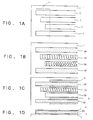
- Figs. 1 show a method for manufacturing colour filters by means of the high-polymer electrodeposition method.
- Fig. 1A shows a glass substrate 1 having a plurality of transparent electrodes 2.
- Colour rendering layers 3R, 3G, 3B are formed successively on the transparent electrodes 2 by using colour rendering terminals 2a, as shown in Fig. 1B. While details of a method of manufacturing colour filters by means of the high-polymer electrodeposition method are described in Japanese Unexamined Patent Publication No. 59-114572, an outline thereof will be described here.
- Methods for manufacturing colour filters include, in addition to the high-polymer electrodeposition method (hereafter referred to as electrodeposition method), the dyeing method, pigment dispersion method and printing method.
- a dye matrix material is applied onto a glass substrate whereon a desired pattern is formed in the dye matrix material by photolithography and then dyed by using a dye, this process being repeated three times in the case of a colour filter having three primary colours, R, G and B (Red, Green and Blue).
- This process is repeated three times in the case of a colour filter having three primary colours, R, G and B, similarly to the case of dyeing method.
- a desired pattern is printed on a glass substrate by means of a printing technology such as offset printing using a coloured high-polymer material prepared by mixing a high-polymer material and a pigment as ink.
- This process is repeated three times in the case of a colour filter having three primary colours, R, G and B, similarly to the case of dyeing method, thereby forming a printed colour filter.
- the high-polymer electrodeposition method is, as described previously, a method for forming colour filters 3 by successive electrodeposition of colour filters 3R, 3G and 3B on transparent electrodes 2 which have been patterned in advance as shown in Fig. 1A. While photolithography technology is employed to form the transparent electrode pattern 2, it is carried out on a glass substrate before forming the colour filter and therefore it can be fabricated without reducing the positioning accuracy of the colour filter. This is because the colour filters 3R, 3G and 3B are formed by electrodeposition method on the transparent electrode pattern 2, and therefore the positioning accuracy of the colour filters 3R, 3G and 3B is determined by the positioning accuracy of the transparent electrode pattern 2 already laid down. This method is characterised by its capability of forming colour filter pattern through so-called self-alignment.
- Colour filters usually have light shielding films 6 formed between different colours.
- the light shielding film is a metal film such as chromium laid down by a film forming method such as sputtering before forming the colour filter, and then formed into the desired light shielding film pattern by photolithography.
- a film forming method such as sputtering before forming the colour filter
- Another widely practised method of forming a light shielding film is one where colour filters of two colours disposed adjacent to each other without using a metal film are laminated or partially overlapped, thereby reducing the light transmittance of the overlapped or laminated region and providing a substitute for the light shielding film.
- the former, metal film, method is employed in colour LCD (Liquid Crystal Display) of active matrix type such as TFT (Thin Film Transistor) which suffers from deterioration of its characteristics due to leakage of light.
- TFT Thin Film Transistor
- the latter method is employed for less expensive TN (Twisted Nematic) or STN (Super Twisted Nematic) LCD.
- an electrodeposited colour filter 3 is formed first as described above with reference to in Figs. 1A and 1B. Then a light shielding film 6 is formed by a back exposure method using the colour filter 3 as the mask.
- This method has the advantage that the light shielding film 6 can be formed by self-alignment similarly to the case of the colour filter 3, because the electrodeposited colour filter 3 can be used as a mask.
- the colour filter 3 is formed on the transparent electrodes 2 which have been patterned beforehand, the light shielding film 6 can be formed only in the gaps of the colour filter 3 as shown in Fig. 1C. It thus has a lower degree of freedom in the configuration of the light shielding film 6.
- Figs. 2 show schematic sectional drawings of a colour LCD of TFT type of the prior art.
- Fig. 2A shows a colour filter substrate 1 disposed to oppose, via a liquid crystal layer 9, transparent electrodes 7 and TFT 8 which are formed on a TFT array substrate 11.
- Fig. 2B is an enlarged drawing of a portion of the TFT array substrate 11 showing the positional relationship between the TFT 8, a colour filter 3 and a light shielding film 6.
- Fig. 2C shows only a portion of the colour filter 3 located at the same position as the portion enclosed by dashed line in Fig. 2B. From these drawings it can be seen that the TFT 8 is covered by the light shielding film 6.
- light shielding films 6 crossing the colour filters 3R, 3G, 3B at right angles are also provided in addition to those provided in the gaps between the colour filters 3R, 3G, 3B, in order to form the light shielding films 6 in a lattice configuration.
- the light shielding film 6 generally plays a role of protecting the TFT 8 elements from deterioration of characteristics due to exposure to light (referred to as light leakage hereafter).
- Light leakage refers to reactions such as, when a thin film of amorphous silicon formed on the TFT 8 elements is exposed to light of a certain intensity, resistance of the amorphous silicon reduces thereby causing voltage which has been retained by the transparent display electrode 7 to be leaked.
- the potential difference between the transparent electrode 4 and the transparent display electrode 7 decreases below the threshold voltage of the liquid crystal 9 causing the liquid crystal 9 to be uncontrollable and leading to display failure.
- the electrodeposited colour filter has the advantage that the colour filter and the light shielding film can be fabricated easily by self-alignment, this advantage in turn causes a problem of inability to form a lattice-shaped light shielding film suited to an active matrix LCD which is subject to deterioration of the characteristics due to light leakage of the TFT.
- the colour filter 3 is formed as continuous stripes following the transparent electrode pattern 2 which is indispensable in forming the electrodeposited colour filter 3 as shown in Figs. 1. Consequently, the configuration of the light shielding film 6 fabricated in the gaps of the colour filter 3 by the back exposure method is also formed in a configuration of stripes.
- Spectral characteristics of the electrodeposited colour filters of three colours, red, green and blue, are shown in Fig. 3. From the spectral characteristics, intensity level of the transmitted light passing through the filters can be understood.
- a lattice-shaped light shielding film 6 When a lattice-shaped light shielding film 6 is not provided, light transmitting through the filters 6 and the liquid crystal layer 9 irradiates the TFT elements 8 as shown in Fig. 2A, thereby causing the problem of deterioration of the TFT element characteristics.
- This invention was intended to provide a method of manufacturing a colour filter overcoming this problem.
- a method of removing a part of a colour filter formed by the high-polymer electrodeposition method before forming a light shielding film is employed.
- this invention provides a method of manufacturing a colour filter on a transparent substrate comprising the following processes:
- this invention provides a method of manufacturing a multiple colour liquid crystal display device including a colour filter mounted on a transparent electrode substrate bearing transparent electrodes for the multiple colour liquid crystal display device comprising the following processes;
- the most effective means for removing a part of the electrodeposited colour filter is to use a laser.
- the reasons for this conclusion are the fact that the positioning accuracy of the colour filter and the light shielding film used in the TFT-LCD is as high as within ⁇ 10 micrometers, and that surface smoothness as high as ⁇ 0.15 micrometers is required for the colour filter surface after removing part of the electrodeposited colour filter.
- a colour filter which does not satisfy at least these two requirements cannot be used for TFT-LCD.
- the high accuracy drive table may be one driven by a stepper motor used in an exposure device or one driven by a linear motor for high-speed drive.
- the corresponding part of the first transparent electrode is also removed simultaneously.
- the colour filter layer and the part of the transparent electrodes used for the formation of the part of the colour filter to be removed are evaporated and dispersed instantaneously, and therefore it causes only an extremely small amount of contamination of the surface. Removal by means of laser is also possible in the case where a protective resin or a second transparent electrode formed on the colour filter exist.
- a local suction device may be installed near the portion of the colour filter surface irradiated with laser energy.
- Any kind of laser may be used such as YAG laser, rare gas lasers including xenon laser and He-Ne Laser, and excimer, provided it is able to remove the colour filter and, if necessary, the transparent electrode and any other layers to be removed.
- the method for manufacturing colour filters in the multiple colour liquid crystal display device of the invention described above comprises at least the following processes: a process of patterning transparent electrodes; a process of forming a colour filter on the patterned transparent electrodes; a process of forming a transparent electrode on the colour filter; a process of removing part of the colour filter and part of the transparent electrode; and a process of forming a light shielding film.
- the method for manufacturing colour filters wherein the colour filter is formed on a transparent electrode substrate having transparent electrodes comprising at least the following manufacturing processes: a process of patterning transparent electrodes; a process of forming a colour filter on the patterned transparent electrodes; a process of forming transparent electrodes on the colour filter; a process of removing part of the colour filter and part of the transparent electrodes; and a process of forming a light shielding film.
- the method for manufacturing multiple colour liquid crystal display devices wherein a colour filter is formed on a transparent electrode substrate having transparent electrodes for multiple colour display devices employing the colour filter comprising at least the following manufacturing processes: a process of patterning transparent electrodes; a process of forming a colour filter on the patterned transparent electrodes; a process of forming transparent electrodes on the colour filter; a process of forming a light shielding film.
- Fig. 4 shows a flow chart of a manufacturing process used in one embodiment of the method of manufacturing colour filters according to the invention.
- Figs. 5 show explanatory schematic diagrams for each manufacturing process of the flow chart of Fig. 4.
- a first pattern of transparent electrodes is made (patterning step 1 in Fig. 4) which is required to form a colour filter by means of the high-polymer electrodeposition method (electrodeposited colour filter step 2 in Fig. 4), as shown in Fig. 5A, on a glass substrate 1 whereon first transparent electrodes 2 are installed.
- This patterning process was carried out by means of the photolithography process commonly employed.
- the transparent electrodes were made of indium-tin (ITO) films which were formed by sputtering to have a sheet resistance of 15 ⁇ /m2 and a film thickness of 150nm (1500 Angstrom).
- ITO indium-tin
- a glass substrate 1 bears a transparent electrode pattern 2.
- the transparent electrode pattern 2 is made with electrode patterns 2 in groups of three. The length of each transparent electrode pattern 2 in each group of three is different so that the colour filters of three colours, red, green and blue can be formed successively.
- Each transparent electrode pattern 2 is disposed to extend straight up to other end of the glass substrate 1 and recesses 7 are provided at constant intervals as shown in Fig 5A.
- the interval of the recesses 7 is made to be the same as the interval of pixels of the TFT-LCD used in the multiple colour crystal display device of the invention, and the area of the recesses 7 is made to be equal to or greater than the area of the TFT element on the TFT substrate side.
- the electrodeposited colour filters 3 of three colours, red, green and blue, 3R, 3G and 3B respectively are installed on the transparent electrode pattern 2.
- Fig. 5B shows a schematic sectional diagram through an electrodeposited colour filter 3R provided on a transparent electrode pattern 2.
- the electrodeposited colour filters 3R, 3G and 3B are made to have the same thickness of 1.5 micrometers.
- Fig. 5C shows the glass substrate 1 with the first transparent electrode pattern 2 where the electrodeposited colour filter 3R has been formed over the entire surface thereof whereon a second transparent electrode 4 is formed by sputtering.
- the transparent electrode 4 has a sheet resistance of 50 ⁇ /m2 and a film thickness of 100nm (1000 Angstrom).
- part of the electrodeposited colour filters 3R, 3G and 3B and part of the second transparent electrode 4 were removed by means of a YAG laser (LR-230 made by HOYA) (Irradiating laser step 4 in Fig. 4).
- the parts removed by the laser are the parts overlying the portions of the transparent electrode pattern 2 which are made narrower adjacent the recesses 7 and disposed at constant intervals as shown in Fig. 5A. Depth of removal can be controlled to some extent by adjusting the output of the YAG laser.
- at least the transparent electrode 4 and the electrodeposited colour filters 3R, 3G and 3B must be removed. It is preferable also to remove the transparent electrode 2 for the formation of the electrodeposited colour filter, too.
- the photosensitive resin may be a negative resist which reacts to ultraviolet light irradiated from the back of the glass substrate 1 (back exposure) in consideration of the spectral characteristic of the electrodeposited colour filters 3R, 3G and 3B.
- OFPR800 made by Tokyo Ouka
- photoresist made by Nippon Kayaku and one made by Fuji Hunt may be used.
- the black resist in the gaps of the electrodeposited colour filters is light-hardened and is therefore formed as a light shielding film 6.
- the film thickness of the light shielding film 6 is set to 1.5 micrometers similarly to the electrodeposited colour filter 3. At this time, it is preferred to form the light shielding film 6 not only in the gaps of the electrodeposited colour filters 3 but also around them as shown in Fig. 5D.
- the light shielding film was made by adjusting the optical density (OD value) of the black resist to 2.5 or higher in order to prevent the TFT characteristics from deteriorating due to light leakage.
- the electrodeposited colour filter of the invention provided with the lattice-shaped light shielding film used in the invention was manufactured by the manufacturing method described above and can be used to form the multiple colour liquid crystal display device of the invention.
- Fig. 6 is a flow chart of a manufacturing process showing a second embodiment of the method for manufacturing colour filters according to the invention.
- the manufacturing process uses a process of patterning a transparent electrode pattern 2 for forming an electrodeposited colour filter formed on a glass substrate provided with ITO transparent electrodes by means of the YAG laser used in the first embodiment.
- the transparent electrode 2 was made by vacuum evaporation method to have a sheet resistance of 20 ⁇ /m2 and film thickness of 150nm (1500 Angstrom).
- the patterning of the transparent electrode 2 was carried out by laser to obtain a stripe configuration similar to that shown in Fig. 1, although the shape may be arbitrary as far as the electrodeposited colour filter can be formed (step 1 in Fig. 6).
- electrodeposited colour filters 3R, 3G, 3B were formed on the transparent electrode pattern 2 similarly to the first embodiment.
- Film thickness of the electrodeposited filter was set to 1.2 micrometers for all colours (step 2 in Fig. 6).
- part of the electrodeposited colour filter and part of the transparent electrode 2 were removed by means of a xenon laser (FLOROD LFA) similarly to the first embodiment (step 3 in Fig. 6).
- a black resist was applied onto the surface of the electrodeposited colour filter substrate to form a light shielding film having a film thickness of 1.2 micrometers similarly to the first embodiment (step 4 in Fig. 6).
- a transparent electrode having a sheet resistance of 50 ⁇ /m2 was installed on the surface of the electrodeposited colour filter whereon a light shielding film was formed, thereby completing an electrodeposited colour filter substrate (step 5 in Fig. 6).
- the multiple colour liquid crystal display device of the invention was fabricated similarly to the first embodiment by using the colour filter substrate and the TFT substrate, and no deterioration of the TFT element characteristic due to light leakage was observed at all.
- the electrodeposited colour filter substrate described in this embodiment can be used in a multiple colour liquid crystal display device of simple matrix type, by making the transparent electrode provided on the surface in a desired pattern.
- Fig. 7 is a flow chart of a manufacturing process showing a third embodiment of the method for manufacturing colour filters according to the invention, which may be used in the multiple colour liquid crystal display device of the invention.
- This third embodiment is a variation of the first embodiment wherein the sequence of forming the transparent electrode in the manufacturing process step 3 of the first embodiment and laser irradiation in the manufacturing process step 4 of the first embodiment are interchanged, and is capable of manufacturing the colour filter required by the invention similarly to the first embodiment because the presence of the transparent electrode 4 can be easily compensated for by adjusting the laser output.
- the multiple colour liquid crystal display device of the invention was fabricated similarly to the first embodiment by using the colour filter substrate of the invention and the TFT substrate, and no deterioration of the TFT element characteristic due to light leakage was observed at all.
- the multiple colour liquid crystal display device using the electrodeposited colour filter which is a simplified manufacturing method can be made at lower cost than the multiple colour liquid crystal display devices using colour filters made by other manufacturing methods which require expensive manufacturing facilities and complicated processes.
Landscapes
- Physics & Mathematics (AREA)
- Nonlinear Science (AREA)
- Mathematical Physics (AREA)
- Chemical & Material Sciences (AREA)
- Crystallography & Structural Chemistry (AREA)
- General Physics & Mathematics (AREA)
- Optics & Photonics (AREA)
- Optical Filters (AREA)
- Liquid Crystal (AREA)
Applications Claiming Priority (6)
| Application Number | Priority Date | Filing Date | Title |
|---|---|---|---|
| JP31625/94 | 1994-03-01 | ||
| JP3162594 | 1994-03-01 | ||
| JP3162594 | 1994-03-01 | ||
| JP15244094A JPH07294725A (ja) | 1994-03-01 | 1994-07-04 | カラーフィルター及び多色液晶表示装置の製造方法 |
| JP152440/94 | 1994-07-04 | ||
| JP15244094 | 1994-07-04 |
Publications (2)
| Publication Number | Publication Date |
|---|---|
| EP0670509A1 true EP0670509A1 (de) | 1995-09-06 |
| EP0670509B1 EP0670509B1 (de) | 2000-07-19 |
Family
ID=26370132
Family Applications (1)
| Application Number | Title | Priority Date | Filing Date |
|---|---|---|---|
| EP95301313A Expired - Lifetime EP0670509B1 (de) | 1994-03-01 | 1995-03-01 | Verfahren zur Herstellung eines Farbfilters und mehrfarbige Flüssigkristallgeräte |
Country Status (6)
| Country | Link |
|---|---|
| US (1) | US5684553A (de) |
| EP (1) | EP0670509B1 (de) |
| JP (1) | JPH07294725A (de) |
| KR (1) | KR100191472B1 (de) |
| CN (1) | CN1072807C (de) |
| DE (1) | DE69518028T2 (de) |
Cited By (1)
| Publication number | Priority date | Publication date | Assignee | Title |
|---|---|---|---|---|
| EP0807846A3 (de) * | 1996-05-16 | 2000-03-01 | TryOnics Corporation | Farbanzeigevorrichtung und Verfahren zur deren Herstellung |
Families Citing this family (14)
| Publication number | Priority date | Publication date | Assignee | Title |
|---|---|---|---|---|
| KR0182015B1 (ko) * | 1994-11-28 | 1999-05-01 | 김광호 | 액정 표시장치용 칼라필터의 제조 방법 |
| US5853924A (en) * | 1994-12-26 | 1998-12-29 | Alps Electric Co., Ltd. | Method of manufacturing color filters |
| JPH09152507A (ja) * | 1995-03-29 | 1997-06-10 | Seiko Instr Inc | 多色液晶表示装置の製造方法 |
| US6900855B1 (en) * | 1995-10-12 | 2005-05-31 | Semiconductor Energy Laboratory Co., Ltd. | Display device having resin black matrix over counter substrate |
| KR100466396B1 (ko) * | 1995-12-30 | 2005-04-08 | 비오이 하이디스 테크놀로지 주식회사 | 발광형액정표시장치 |
| US6208394B1 (en) * | 1997-11-27 | 2001-03-27 | Sharp Kabushiki Kaisha | LCD device and method for fabricating the same having color filters and a resinous insulating black matrix on opposite sides of a counter electrode on the same substrate |
| JP4215905B2 (ja) * | 1999-02-15 | 2009-01-28 | シャープ株式会社 | 液晶表示装置 |
| JP3576871B2 (ja) * | 1999-06-04 | 2004-10-13 | 日本電気株式会社 | アクティブマトリクス型液晶表示装置 |
| US7310124B2 (en) * | 2003-05-09 | 2007-12-18 | Sharp Kabushiki Kaisha | Color filter substrate, method of manufacturing the color filter and display device |
| US20040245225A1 (en) * | 2003-06-04 | 2004-12-09 | Alexander Kastalsky | Making color in two - and three - dimensional images created in glass with laser induced micro-explosions |
| US7294372B2 (en) * | 2003-10-01 | 2007-11-13 | Eastman Kodak Company | Conductive color filters |
| US20070287080A1 (en) * | 2006-06-08 | 2007-12-13 | Orbotech Ltd | Enhancement of inkjet-printed elements using photolithographic techniques |
| JP2008026752A (ja) * | 2006-07-24 | 2008-02-07 | Nec Lcd Technologies Ltd | カラーフィルタ基板、カラーフィルタ基板の修正方法及びカラー液晶表示装置 |
| JP2010080224A (ja) * | 2008-09-25 | 2010-04-08 | Sony Corp | 光学部品の製造方法および光学部品、並びに表示装置の製造方法および表示装置 |
Citations (2)
| Publication number | Priority date | Publication date | Assignee | Title |
|---|---|---|---|---|
| EP0317063A2 (de) * | 1987-11-18 | 1989-05-24 | International Business Machines Corporation | Farb-Flüssigkristall-Anzeigevorrichtung und ihr Herstellungsverfahren |
| EP0501657A1 (de) * | 1991-02-25 | 1992-09-02 | Seiko Instruments Inc. | Verfahren zur Herstellung eines Farbfilters |
Family Cites Families (8)
| Publication number | Priority date | Publication date | Assignee | Title |
|---|---|---|---|---|
| US4006968A (en) * | 1975-05-02 | 1977-02-08 | Hughes Aircraft Company | Liquid crystal dot color display |
| EP0184341B1 (de) * | 1984-11-12 | 1994-01-26 | Semiconductor Energy Laboratory Co., Ltd. | Flüssigkristallanzeigeschirm und Verfahren zu seiner Herstellung |
| DE3674547D1 (de) * | 1985-11-26 | 1990-10-31 | Stanley Electric Co Ltd | Fluessigkristall-farbanzeigevorrichtung und verfahren zu ihrer herstellung. |
| JP2593670B2 (ja) * | 1987-11-26 | 1997-03-26 | セイコー電子工業株式会社 | カラー表示装置の製造方法 |
| JPH04301604A (ja) * | 1991-03-29 | 1992-10-26 | Toshiba Corp | カラーフィルタおよびその製造方法およびこれを用いた液晶表示装置 |
| JP3350991B2 (ja) * | 1992-03-06 | 2002-11-25 | セイコーエプソン株式会社 | 電気光学装置用基板、及び電気光学装置 |
| JP2944854B2 (ja) * | 1993-06-29 | 1999-09-06 | シャープ株式会社 | 液晶素子の製造方法 |
| US5340619A (en) * | 1993-10-18 | 1994-08-23 | Brewer Science, Inc. | Method of manufacturing a color filter array |
-
1994
- 1994-07-04 JP JP15244094A patent/JPH07294725A/ja active Pending
-
1995
- 1995-02-28 US US08/395,442 patent/US5684553A/en not_active Expired - Lifetime
- 1995-02-28 KR KR1019950004291A patent/KR100191472B1/ko not_active Expired - Fee Related
- 1995-03-01 DE DE69518028T patent/DE69518028T2/de not_active Expired - Fee Related
- 1995-03-01 CN CN95103249A patent/CN1072807C/zh not_active Expired - Fee Related
- 1995-03-01 EP EP95301313A patent/EP0670509B1/de not_active Expired - Lifetime
Patent Citations (2)
| Publication number | Priority date | Publication date | Assignee | Title |
|---|---|---|---|---|
| EP0317063A2 (de) * | 1987-11-18 | 1989-05-24 | International Business Machines Corporation | Farb-Flüssigkristall-Anzeigevorrichtung und ihr Herstellungsverfahren |
| EP0501657A1 (de) * | 1991-02-25 | 1992-09-02 | Seiko Instruments Inc. | Verfahren zur Herstellung eines Farbfilters |
Non-Patent Citations (2)
| Title |
|---|
| K. TSUDA: "Colour filters for LCDs", DISPLAYS, vol. 14, JORDAN HILL, GB, pages 115 - 124, XP000397434, DOI: doi:10.1016/0141-9382(93)90078-J * |
| S. YAMAUCHI ET AL.:: "Homeotropic-Alignment Full-Color LCD", 1989 SID INTERNATIONAL SYMPOSIUM, DIGEST OF TECHNICAL PAPERS, vol. 20, BALTIMORE, USA, pages 378 - 381, 438 * |
Cited By (1)
| Publication number | Priority date | Publication date | Assignee | Title |
|---|---|---|---|---|
| EP0807846A3 (de) * | 1996-05-16 | 2000-03-01 | TryOnics Corporation | Farbanzeigevorrichtung und Verfahren zur deren Herstellung |
Also Published As
| Publication number | Publication date |
|---|---|
| CN1072807C (zh) | 2001-10-10 |
| KR100191472B1 (ko) | 1999-06-15 |
| US5684553A (en) | 1997-11-04 |
| JPH07294725A (ja) | 1995-11-10 |
| EP0670509B1 (de) | 2000-07-19 |
| DE69518028T2 (de) | 2000-12-21 |
| DE69518028D1 (de) | 2000-08-24 |
| CN1116714A (zh) | 1996-02-14 |
Similar Documents
| Publication | Publication Date | Title |
|---|---|---|
| EP0670509B1 (de) | Verfahren zur Herstellung eines Farbfilters und mehrfarbige Flüssigkristallgeräte | |
| US6043857A (en) | Liquid crystal display apparatus | |
| KR100724478B1 (ko) | 액정표시소자 제조방법 | |
| EP0536680B1 (de) | Flüssigkristallvorrichtung und Verfahren zum Einfüllen des Flüssigkristalls | |
| KR100262376B1 (ko) | 액정표시장치및그제조방법 | |
| US5682215A (en) | Color display device with light incident substrate having color filters on the outside and microlenses on the inside surface | |
| EP0570176A1 (de) | Flüssigkristallanzeigetafel und Verfahren zu ihrer Herstellung | |
| US6323920B1 (en) | Methods of making LCD devices having color filter | |
| KR100469561B1 (ko) | 액정표시장치용 컬러필터 기판 제조 방법 | |
| US20050095514A1 (en) | Method of fabricating color filter panel using back exposure and structure of color filter panel | |
| KR100845256B1 (ko) | 액정표시소자의 제조방법 | |
| US5008166A (en) | Method for manufacturing a color filter | |
| US6914263B2 (en) | Color filter substrate having a panel identification and manufacturing method thereof | |
| JPH0527111A (ja) | カラー液晶表示装置におけるカラーフイルタの欠陥修正方法 | |
| US20070229735A1 (en) | Method for manufacturing liquid crystal display and liquid crystal display manufactured thereby | |
| JPH08327996A (ja) | 液晶表示装置の製造方法 | |
| JPH0815523A (ja) | カラーフィルター及び多色液晶表示装置の製造方法 | |
| KR100233072B1 (ko) | 칼라필터 제조방법 | |
| KR100453366B1 (ko) | 액정패널의제조방법 | |
| JPH08320482A (ja) | 液晶表示素子の加工方法 | |
| KR20080030912A (ko) | 액정표시장치용 기판 및 그 제조 방법 | |
| KR100202233B1 (ko) | 컬러필터어레이의 제조방법 | |
| KR100400163B1 (ko) | 저반사 칼라필터기판의 제조방법 | |
| JPH0668591B2 (ja) | 液晶装置用電極基板の製造方法 | |
| KR20040053667A (ko) | 액정표시장치의 컬러필터 기판 및 이의 제작방법 |
Legal Events
| Date | Code | Title | Description |
|---|---|---|---|
| PUAI | Public reference made under article 153(3) epc to a published international application that has entered the european phase |
Free format text: ORIGINAL CODE: 0009012 |
|
| AK | Designated contracting states |
Kind code of ref document: A1 Designated state(s): DE FR GB |
|
| 17P | Request for examination filed |
Effective date: 19960306 |
|
| 17Q | First examination report despatched |
Effective date: 19980811 |
|
| GRAG | Despatch of communication of intention to grant |
Free format text: ORIGINAL CODE: EPIDOS AGRA |
|
| RTI1 | Title (correction) |
Free format text: METHOD FOR MANUFACTURING COLOUR FILTERS AND MULTIPLE COLOUR LIQUID CRYSTAL DISPLAY DEVICES |
|
| RTI1 | Title (correction) |
Free format text: METHOD FOR MANUFACTURING COLOUR FILTERS AND MULTIPLE COLOUR LIQUID CRYSTAL DISPLAY DEVICES |
|
| GRAG | Despatch of communication of intention to grant |
Free format text: ORIGINAL CODE: EPIDOS AGRA |
|
| GRAH | Despatch of communication of intention to grant a patent |
Free format text: ORIGINAL CODE: EPIDOS IGRA |
|
| GRAH | Despatch of communication of intention to grant a patent |
Free format text: ORIGINAL CODE: EPIDOS IGRA |
|
| GRAA | (expected) grant |
Free format text: ORIGINAL CODE: 0009210 |
|
| AK | Designated contracting states |
Kind code of ref document: B1 Designated state(s): DE FR GB |
|
| ET | Fr: translation filed | ||
| REF | Corresponds to: |
Ref document number: 69518028 Country of ref document: DE Date of ref document: 20000824 |
|
| PLBE | No opposition filed within time limit |
Free format text: ORIGINAL CODE: 0009261 |
|
| STAA | Information on the status of an ep patent application or granted ep patent |
Free format text: STATUS: NO OPPOSITION FILED WITHIN TIME LIMIT |
|
| 26N | No opposition filed | ||
| REG | Reference to a national code |
Ref country code: GB Ref legal event code: IF02 |
|
| PGFP | Annual fee paid to national office [announced via postgrant information from national office to epo] |
Ref country code: GB Payment date: 20030226 Year of fee payment: 9 |
|
| PGFP | Annual fee paid to national office [announced via postgrant information from national office to epo] |
Ref country code: FR Payment date: 20030310 Year of fee payment: 9 |
|
| PGFP | Annual fee paid to national office [announced via postgrant information from national office to epo] |
Ref country code: DE Payment date: 20030313 Year of fee payment: 9 |
|
| PG25 | Lapsed in a contracting state [announced via postgrant information from national office to epo] |
Ref country code: GB Free format text: LAPSE BECAUSE OF NON-PAYMENT OF DUE FEES Effective date: 20040301 |
|
| PG25 | Lapsed in a contracting state [announced via postgrant information from national office to epo] |
Ref country code: DE Free format text: LAPSE BECAUSE OF NON-PAYMENT OF DUE FEES Effective date: 20041001 |
|
| GBPC | Gb: european patent ceased through non-payment of renewal fee | ||
| PG25 | Lapsed in a contracting state [announced via postgrant information from national office to epo] |
Ref country code: FR Free format text: LAPSE BECAUSE OF NON-PAYMENT OF DUE FEES Effective date: 20041130 |
|
| REG | Reference to a national code |
Ref country code: FR Ref legal event code: ST |