EP0670635A2 - PLL-Oszillator, Schaltung zur fortlaufenden Mittelwertbildung sowie Teilerverhältnis-Entzerrerschaltung - Google Patents
PLL-Oszillator, Schaltung zur fortlaufenden Mittelwertbildung sowie Teilerverhältnis-Entzerrerschaltung Download PDFInfo
- Publication number
- EP0670635A2 EP0670635A2 EP95103054A EP95103054A EP0670635A2 EP 0670635 A2 EP0670635 A2 EP 0670635A2 EP 95103054 A EP95103054 A EP 95103054A EP 95103054 A EP95103054 A EP 95103054A EP 0670635 A2 EP0670635 A2 EP 0670635A2
- Authority
- EP
- European Patent Office
- Prior art keywords
- circuit
- frequency
- value
- output
- phase
- Prior art date
- Legal status (The legal status is an assumption and is not a legal conclusion. Google has not performed a legal analysis and makes no representation as to the accuracy of the status listed.)
- Granted
Links
Images


Classifications
-
- H—ELECTRICITY
- H03—ELECTRONIC CIRCUITRY
- H03L—AUTOMATIC CONTROL, STARTING, SYNCHRONISATION OR STABILISATION OF GENERATORS OF ELECTRONIC OSCILLATIONS OR PULSES
- H03L7/00—Automatic control of frequency or phase; Synchronisation
- H03L7/06—Automatic control of frequency or phase; Synchronisation using a reference signal applied to a frequency- or phase-locked loop
- H03L7/08—Details of the phase-locked loop
- H03L7/099—Details of the phase-locked loop concerning mainly the controlled oscillator of the loop
- H03L7/0991—Details of the phase-locked loop concerning mainly the controlled oscillator of the loop the oscillator being a digital oscillator, e.g. composed of a fixed oscillator followed by a variable frequency divider
- H03L7/0992—Details of the phase-locked loop concerning mainly the controlled oscillator of the loop the oscillator being a digital oscillator, e.g. composed of a fixed oscillator followed by a variable frequency divider comprising a counter or a frequency divider
Definitions
- the present invention relates to a phase-locked loop oscillator for generating an output clock signal synchronized to an input clock signal and substantially free from phase variations of the input clock, and also relates to a moving-average circuit, and a division-ratio equalization circuit, suitable for use in the same. More particularly, the invention relates to a phase-locked loop oscillator for generating, from a fixed-frequency oscillator output, an output clock signal synchronized to an input clock signal, and substantially free from phase variations of the input clock, by uniformly controlling a dual-modulus frequency divider that operates with a division ratio selected from two division ratios, and also relates to a moving-average circuit, and a division-ratio equalization circuit, suitable for use in the same.
- synchronous multiplexing transmission systems such as SDH (synchronous digital hierarchy) and SONET (synchronous optical network) systems
- a highly stable clock signal that serves as a reference for network synchronization, is transmitted from a master station to a slave station, and further to the next slave station and so on.
- Each slave station receives the clock signal transmitted from the master station or from another slave station on the master station side, and generates a synchronized clock signal for transmission to the next slave station.
- phase-locked loop oscillator in each slave station must have phase lock characteristics that can suppress the jitter and wander contained in the clock signal input from the transmission channel and that allows a sufficiently stable clock signal to be transmitted to the next slave station.
- phase variations with a frequency greater than 10 Hz are defined as wander, and those with a frequency less than 10 Hz are defined as jitter.
- phase-locked loop oscillator applicable to the latter system. More specifically, the phase-locked loop oscillator contemplated in the invention is aimed at satisfying the following requirements: capture-frequency range is ⁇ 20 ppm; short-term stability is 5 x 10 ⁇ 9, that is, the ratio of wander amplitude of output clock to wander amplitude of input clock is 5 x 10 ⁇ 9 or less; resistance to jitter is 1.5 UI, 10 - 150 Hz, that is, the phase variation of the output clock is held within the specified value when jitter with amplitude 1.5 times the clock cycle is input within the frequency range of 10 to 150 Hz; and compactness.
- phase-locked loop oscillator in a first phase-locked loop, the phase of the output obtained by dividing a fixed-frequency oscillator output by a dual-modulus frequency divider with a division ratio of N or N+1 is compared with the phase of an input clock signal; at each comparison, if there is a phase lag, the division ratio is set to N (advance control in the first loop), and conversely, if there is a phase lead, the division ratio is set to N+1 (delay control in the first loop).
- the number of advance control events is counted over a predetermined period of time, and the moving average of the count values is taken,
- the moving average value for the number of advance control events in the first loop corresponds to the mean frequency of the input clock signal.
- This moving average value is used to calculate control values for advance control and delay control in a second loop.
- the same fixed-oscillator output used in the first phase-locked loop is frequency-divided by a second dual-modulus frequency divider.
- the output of the divider is phase-compared with the input clock; if there is a lag, the control value for the advance control is selected, and if there is a lead, the control value for the delay control is selected.
- a control signal for controlling the second dual-modulus frequency divider is created from the selected control value, and the control signal is supplied to the frequency divider.
- the input clock and output clock are phase-compared; however, only phase lag or phase lead information is reflected in the control, and the amount of phase difference is not measured and, therefore, is not reflected in the control.
- a possible configuration would be to connect a required number of latch circuits in series and add the values latched in the latch circuits using adders (no dividers are needed if the required number is 2 n ). In this configuration, however, if the number of latch circuit stages is increased, the number of adder circuits required will also increase. For example, if the number of latch circuit stages is n and the number of bits is 20, then a number, (n-1), of 20-bit parallel adders will have to be provided.
- a division-ratio equalization circuit needs to be provided which, based on the control value, performs control for the division ratio to be distributed at equally spaced intervals along the time axis so that the dual-modulus frequency divider outputs a clock signal free from jitter and wander.
- a phase-locked loop oscillator comprising: means for obtaining a first digital value indicating a mean frequency of an input signal; means for obtaining a second digital value indicating a mean phase difference of an output signal relative to the input signal; means for calculating a control value on the basis of the first and second digital values; a dual-modulus frequency divider for generating the output signal by frequency-dividing a reference signal, the frequency divider being capable of operating with a division ratio selected from two division ratios in accordance with a control signal; and means for generating the control signal for controlling the dual-modulus frequency divider in accordance with the control value.
- a moving-average circuit comprising: a storage circuit for storing a predetermined number of successive numeric values, and for outputting in sequence all the numeric values stored therein each time the stored contents thereof are updated with entry of a new numeric value; and an accumulator circuit for successively adding up the numeric values serially output from the storage circuit, the accumulator circuit being cleared when the stored contents of the storage circuit is updated.
- a division-ratio equalization circuit for generating a control signal by which a dual-modulus frequency divider, capable of operating with a division ratio selected from two division ratios in accordance with a control signal, is controlled so that the division ratio is distributed at equally spaced intervals along the time axis in accordance with an input control value, comprising: a calculating circuit that, from the input control value, successively calculates quotients a0, a1, a2 ⁇ a m for output, when the control value is expressed as 1 / (a0 + 1 / (a1 + 1 / (a2 + ⁇ + 1 /a m )) ⁇ ) , and a control signal generating circuit that includes a cascaded chain of a plurality of programmable frequency dividers in which the plurality of quotients a0, a1, a2 ⁇ a m are set as respective division ratios, and that frequency-divides a reference signal through the cascade
- Figure 1 shows a simplified schematic of a phase-locked loop oscillator according to the present invention.
- a reference clock signal (for example, a 51.84-MHz signal) from a reference oscillator (not shown) is frequency-divided by a dual-modulus frequency divider 10 whose division ratio is set to either N or N+1 (N is an integer, for example, 33) in accordance with a control signal.
- the output of the frequency divider 10 is phase-compared in a phase comparator 12 with an input clock signal (for example, a 1.544-MHz signal); at each comparison, if there is a phase lag, the division ratio of the frequency divider 10 is set to N (advance control), and if there is a phase lead, it is set to N+1 (delay control).
- the number of advance control events (or delay control events) during a predetermined period of time is counted by a counter circuit 14. If the operating clock frequency of the phase comparator 12 (for example, the output of the frequency divider 10 is used) is taken as the reference for time, the total number of advance control and delay control events during the predetermined period of time is constant (in the above example, 772,000); therefore, it is only necessary to count the number of events of one or the other of the two control types (in this example, the number of advance control events is counted).
- the number of advance control events counted by the counter circuit 14 is fed to a moving-average circuit 16 which calculates the moving average, for example, over 16 seconds, i.e., over 32 successive samples.
- the moving average of the number of advance control events corresponds to the mean frequency of the input clock signal.
- the center control value for the number of advance control events is calculated by a center control value calculator 18 from the moving average value for the number of advance control events supplied from the moving-average circuit 16. Details of the center control value calculation will be described later.
- the reference clock signal is also input to a frequency divider 20, which has the same configuration as the frequency divider 10.
- the input clock frequency is divided, as in the frequency divider 10, and the output of the frequency divider 20 is fed to a phase comparator 22 for phase comparison with the input clock signal.
- the phase comparator 22 outputs a pulse indicating an advance period or delay period. With these pulses as a gate signal, a phase difference measuring circuit 24 counts master clock pulses and produces a digital signal indicating a phase difference.
- the values of the phase differences output from the phase difference measuring circuit 24 are fed into a moving-average circuit 26 for calculation of the moving average. The result is multiplied in a gain controller 28 by a "phase gain".
- the result of the multiplication is fed to an adder 30 where it is added to the center control value output from the center control value calculator 18, and the final control value for the number of advance control events is obtained.
- a constant ⁇ for example, 3
- ⁇ for example, 3
- division-ratio equalization circuit 32 and 34 which generate respective control signals.
- a selector 36 a - ⁇ signal is selected when the mean phase difference is positive, and a + ⁇ signal when it is negative and the thus selected control signal is applied to the frequency divider 20.
- An alarm control circuit 38 detects an out-of-synchronization alarm, and when the alarm is detected, control is based only on the mean frequency.
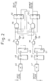
- FIG. 2 shows the configuration of the phase comparator 22.
- the frequencies of the input clock and output clock (for example, 1.544 MHz) are first divided by M (for example, 16) in frequency dividers 46 and 47 respectively, and then, their phases are compared.
- D flip-flops 48 - 51, JK flip-flops 52 and 53, AND gates 54 - 57, and inverters 58 and 59 constitute a known synchronous-type phase comparator.
- a synchronous-type phase comparator is employed here for stable circuit operation.
- Figure 3 shows the configuration of the phase difference measuring circuit 24. Since the delay period pulse and the advance period pulse do not occur simultaneously, the two outputs are ORed by an OR gate 60 whose output is fed to a counter 61. This configuration allows the use of only one counter to serve the purpose. Using the signal from the OR gate 60 as a gate signal, the counter 61 counts master clock pulses (for example, 51.84 MHz) to measure the amount of the phase difference. The count value of the counter 61 is fed into a latch 62 by the control signal synchronized to the phase comparison timing, after which the counter 61 is reset.
- master clock pulses for example, 51.84 MHz
- the measured phase difference value output from the phase difference measuring circuit 24 is given in the form of an absolute value without a positive or negative sign
- addition is performed in the moving-average circuit 26 at the subsequent stage (see Figure 1) by appending an appropriate sign.
- the moving average is calculated after pereforming integration over a period of 4,096 samples (equivalent to 0.0424 second). Since the measured phase difference value latched in the latch 62 corresponds to an instantaneous value of the jitter amplitude, it is compared in a comparator 63 with constant values.
- Signals designated A ⁇ 7 and A ⁇ 12 indicate that the phase error is 100 ns or greater and 200 ns or greater, respectively, when the master clock is 51.84 Mhz; these signals are used for switching the number of moving-average samples in the moving-average circuit 26, as will be described later.
- Signal designated A ⁇ 136 indicates that the phase error is 2585 ns (which corresponds to 0.25 UI);this signal is used for detection of an out-of-synchronization condition.
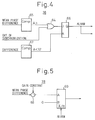
- Figure 4 illustrates the configuration of the alarm control circuit 38 shown in Figure 1.
- the instantaneous out-of-synchronization signal described with reference to Figure 3 is applied to one input of an OR gate 64.
- the mean phase difference value output from the moving-average circuit 26 ( Figure 1) is compared in a comparator 65 with a predetermined value, and the result is fed to the other input of the OR gate 64.
- the output of the OR gate 64 goes high, which causes a JK flip-flop 66 to change state and output an alarm condition.
- Figure 5 shows the configuration of the gain controller 28 ( Figure 1).
- the mean phase difference output from the moving-average circuit 26 is input to a divider 68 which divides it by a predetermined gain constant and outputs the result to a selector 69. Since the division is supposed to provide an integer value, the result is 0 when the mean phase difference is smaller than the gain constant. When no alarm is issued, the selector 69 selects the result of the division for output to the adder 30 ( Figure 1). When an alarm occurs, since the value of the mean phase difference does not have any meaning, the selector 69 selects a value "0", so that control is performed only by the mean frequency. At this time, the data within the moving-average circuit 26 is cleared.
- Figure 6 shows the configuration of the center control value calculator 18 ( Figure 1).
- a subtractor 70 the difference between the moving average value supplied from the moving-average circuit 16 ( Figure 1) and the previous center control value latched in a latch circuit 71 is calculated, and is fed to a divider 72 where the difference is divided by a predetermined gain constant. When the difference value is smaller than the gain constant, the result is replaced by 1. The result of the division is fed to one input of a selector 73. A constant 0 or 1 is applied at the other input of the selector 73. The value selected by the selector 73 is added in an adder 74 to the previous center control value and then fed to the latch circuit 71.
- a signal indicating that the difference value is positive and a signal indicating that the mean phase difference is positive are input to an AND gate 75, while a signal indicating that the difference value is negative and a signal indicating that the mean phase difference is negative are input to an AND gate 76.
- the outputs of the AND gates 75 and 76 are input to an OR gate 77.
- An alarm signal is applied to the remaining input of the OR gate 77.
- the output of the OR gate 77 is sent to the selector 73 as a control signal.
- Figure 7 shows a plot of the amplitude of jitter, appearing at the output for input jitter of various magnitudes, as a function of the moving-average sample length. The graph of Figure 7 was obtained by computer simulation.
- Figure 8 shows the design of the moving-average sample length control based on the above concept.
- 0.34 second is selected for the moving-average sample length. If it is judged by the comparator 63 of Figure 3 that the phase difference measured value is 7 or greater (which corresponds to input jitter of 0.3 UI or greater), the selection of 0.34 second is inhibited and 0.68 second is selected. Once 0.68 second has been selected, even if the phase difference measured value falls below 7 the selection does not switch back to the shorter length instantaneously but remains at 0.68 second for one second. If it is judged that the phase difference measured value is 12 or greater (which corresponds to input jitter of 0.6 UI or greater), the selection of 0.68 second is inhibited and 1.02 seconds is selected. Likewise, once 1.02 seconds has been selected, even if the phase difference measured value falls below 12 the selected value is held for one second. As previously described, when the phase difference measured value is 136 or greater, it is judged to be an out-of-synchronization condition.
- the moving-average sample length is controlled based on the amplitude of input Jitter, but alternatively, control may be performed on the basis of the frequency of input jitter in such a manner as to increase the moving-average sample length when the jitter frequency is low.
- the input jitter frequency can be measured by detecting zero-cross points of the phase difference measured value. In this case, since there is a possibility of erroneous detection of zero-cross points when the phase difference is very small, hysteresis is introduced in the detection.
- Figure 9 shows the detailed configuration of the moving-average circuit 16 or 26 according to the present invention.
- the circuit shown here is for calculating the moving average of four successive samples.
- n-bit latch circuits 80, 82, 84, and 86 are connected in series.
- An input of the first-stage circuit 80 is connected to the output of a selector 88, and the output of the final-stage circuit 96 is connected to one input ("A" input) of the selector 88.
- the other input (“B" input) of the selector 88 is connected to an input data line.
- the output of the final-stage circuit 86 is also connected to one input of an adder 90.
- the output of the adder 90 is connected to an input of an n-bit latch circuit 92 whose output is connected to the other input of the adder 90.
- the output of the adder 90 is also connected to an n-bit latch circuit 94 whose output is connected to a divider 96.
- a loop-enable signal line is connected to a select input of the selector 88.
- the loop-enable signal line is also connected to an input of an OR gate 98 whose other input is connected to a memory-update signal line.
- the output of the OR gate 98 is connected to an enable input of each of the n-bit latch circuits 80, 82, 84, and 86.
- a reset input and an enable input of the n-bit latch circuit 92 are connected to a reset signal line and a shift-enable signal line, respectively.
- An enable input of the n-bit latch circuit 94 is connected to a latch signal line.
- Clock inputs of the n-bit latch circuits 80, 82, 84, 86, and 92 are connected to a clock signal line.
- Figure 10 is a timing chart for explaining the operation of the moving-average circuit. Signal states at points indicated by reference signs (i) to (xiv) in Figure 9 are shown in (i) to (xiv) in Figure 10. The operation of the moving-average circuit of the present invention will be described below with reference to Figures 9 and 10. It is assumed here that, initially, data "C”, "B”, and “A” are held in the n-bit latch circuits 80, 82, and 84, respectively, and that the input data is "D”. It is also assumed that the n-bit latch circuit 92 is reset and holds data "0".
- the memory update signal (ii) goes low immediately after the positive going transition of the clock signal. Since "0" is held in the n-bit latch circuit 92 (xii), the adder 90 outputs "A" (xiii). The above is the memory update operation.
- a loop operation is initiated at the next positive going transition of the clock signal, immediately after which the loop enable signal (iii) and the shift enable signal (iv) go high and the output of the OR gate 98 returns to high.
- the selector 88 selects the output of the final-stage n-bit latch circuit 86 applied at its A input.
- the n-bit latch circuit 92 also is enabled.
- the contents of the latch circuits 80, 82, 84, and 86 are shifted circularly via the selector 88 and the data "B" is output from the final-stage n-bit latch circuit 86.
- the adder 90 outputs "A+B" (xiii).
- the contents of the latch circuits 80, 82, 84, and 86 are further shifted circularly via the selector 88, and the data "C” and "D” are serially output from the final-stage n-bit latch circuit 92.
- the adder 90 outputs "A+B+C+D" (xiii).
- the shift enable signal (iv) goes low to disable the n-bit latch circuit 92; on the other hand, the latch signal (vi) goes high to enable the n-bit latch circuit 94. Further, the reset signal (vii) goes low (active).
- the output of the adder 90 "A+B+C+D"
- the n-bit latch circuit 92 is reset to "0" (xii).
- Figure 11 shows the configuration of the division-ratio equalization circuit 32 or 34.
- the quotients a0, a1, a2 ⁇ a m are supplied to a control signal generating circuit 102 which sets the quotients as division ratios in programmable frequency dividers connected in cascade, and provides the frequency-divided output as a division-ratio control signal.
- Figure 12 is a diagram showing the configuration of the calculating circuit 100.
- a dividend input of a division circuit 104 is connected to the output of a latch circuit 106, while a divisor input thereof is connected to the output of a latch circuit 108.
- the input of the latch circuit 106 is connected to the output of a selector 110, and the input of the latch circuit 108 is connected to the output of a selector 112.
- the selector 110 selects and outputs one or the other of its two inputs, the total number of control events (fixed value) or the output of the latch circuit 108.
- the selector 112 selects one or the other of its two inputs, the control value for the number of advance control events or a remainder output of the division circuit 104.
- a quotient output of the division circuit 104 is connected to latch circuits 114, 116, 118.
- the selectors 110 and 112 select their A inputs, so that the total number of control events and the control value for the number of advance control events are latched in the latch circuits 106 and 108, respectively.
- the division circuit 104 performs division, the dividend being the total number of Control events supplied from the latch circuit 106 and the divisor being the number of advance control events, and outputs the quotient a0 and the remainder.
- the quotient a0 is latched into the latch circuit 114.
- the selectors 110 and 112 select their B inputs, and the divisor and remainder from the previous division are latched into the latch circuits 106 and 108 as the dividend and the divisor, respectively.
- the division circuit 104 performs division using the thus input dividend and divisor, and outputs the quotient a1 and the remainder.
- the quotient a1 is latched into the latch circuit 116. By repeating this process until the remainder output from the division circuit 104 becomes 0, the quotients a0, a1, a2 ⁇ a m are latched for output.
- the division circuit 104 may be so constructed as to repeatedly subtract the input divisor from the input dividend until the result becomes a negative number and further subtraction becomes impossible, and to output the number of subtraction operations as the quotient and the final difference as the remainder.
- Figure 13 illustrates the configuration of the control signal generating circuit 102 shown in Figure 11.
- the quotients a0, a1, a2 ⁇ a m from the calculating circuit 100 are set as respective division ratios in the programmable frequency dividers D0, D1, D2 ⁇ D m . Since the maximum value of m can be determined when the total number of control events is given, as many programmable frequency dividers as necessary can be provided.
- a reference signal is input to the frequency divider D0 in which the quotient a0 is set, and its frequency-divided output d0 is output as the division-ratio control signal.
- the frequency-divided output d0 is also input to the frequency-divider D1 in which the quotient a1 is set as the division ratio.
- the division ratio of the divider D0 is periodically changed from a0 to a0 + 1. More specifically, during the period that a carry is output after the frequency divider D1 has counted the divide-by value a1 (or a1 + 1), the division ratio of the frequency divider D0 is changed to a0 + 1.
- the frequency-divided output d1 is also input to the frequency divider D2 as an input to be divided.
- the frequency-divided output d i-1 of the frequency divider D i-1 is input to the frequency divider D i (2 ⁇ i ⁇ m-1) with whose frequency-divided output d i the division ratio of the divider D i-1 is periodically changed from a i-1 to a i-1 + 1.
- the frequency-divided output d i is also input to the frequency divider D i+1 as an input to be divided.
- the frequency-divided output d m-1 from the frequency divider D m-1 is input, but its division ratio a m remains unchanged until the value of a m is updated.
- Downward arrows each indicate the generation of a carry upon which the one-stage lower frequency divider counts up
- upward arrows each indicate the generation of a carry upon which the advance control is performed (in the case of the frequency divider D0) or the divide-by value in the one-stage higher frequency divider is increased by 1.
- Figure 16 shows only 16 clock cycles, but this pattern is repeated. As can be seen from the figure, the advance control events are uniformly distributed among the 16 control events.
- the clock signal output from the frequency divider 20 ( Figure 1) is obtained by dividing the input, for example, a 51.84-MHz signal, by 33 or 34, the output clock signal contains jitter equivalent to one phase period (19.29 ns) of 51.84 MHz.
- this jitter consists only of high-frequency components, and therefore, can be eliminated by connecting a band-pass filter or an analog PLL circuit at a subsequent stage,
- a protective memory array with a required number of stages be inserted in the moving-average circuit 16, 26 before the moving-average memory.
Landscapes
- Stabilization Of Oscillater, Synchronisation, Frequency Synthesizers (AREA)
Applications Claiming Priority (3)
| Application Number | Priority Date | Filing Date | Title |
|---|---|---|---|
| JP03432494A JP3275222B2 (ja) | 1994-03-04 | 1994-03-04 | 位相同期発振器 |
| JP3432494 | 1994-03-04 | ||
| JP34324/94 | 1994-03-04 |
Publications (3)
| Publication Number | Publication Date |
|---|---|
| EP0670635A2 true EP0670635A2 (de) | 1995-09-06 |
| EP0670635A3 EP0670635A3 (de) | 1997-09-17 |
| EP0670635B1 EP0670635B1 (de) | 2002-07-10 |
Family
ID=12410983
Family Applications (1)
| Application Number | Title | Priority Date | Filing Date |
|---|---|---|---|
| EP95103054A Expired - Lifetime EP0670635B1 (de) | 1994-03-04 | 1995-03-03 | PLL-Oszillator, Schaltung zur fortlaufenden Mittelwertbildung sowie Teilerverhältnis-Entzerrerschaltung |
Country Status (4)
| Country | Link |
|---|---|
| US (1) | US5867544A (de) |
| EP (1) | EP0670635B1 (de) |
| JP (1) | JP3275222B2 (de) |
| DE (1) | DE69527321T2 (de) |
Cited By (1)
| Publication number | Priority date | Publication date | Assignee | Title |
|---|---|---|---|---|
| US7242229B1 (en) | 2001-05-06 | 2007-07-10 | Altera Corporation | Phase locked loop (PLL) and delay locked loop (DLL) counter and delay element programming in user mode |
Families Citing this family (12)
| Publication number | Priority date | Publication date | Assignee | Title |
|---|---|---|---|---|
| US7587012B2 (en) * | 2004-07-08 | 2009-09-08 | Rambus, Inc. | Dual loop clock recovery circuit |
| JP4196902B2 (ja) * | 2004-08-23 | 2008-12-17 | ソニー株式会社 | 印刷媒体の走行装置、この走行装置を備えた印刷装置、印刷媒体の走行速度制御方法及びコンピュータプログラム |
| US8085893B2 (en) | 2005-09-13 | 2011-12-27 | Rambus, Inc. | Low jitter clock recovery circuit |
| JP5134779B2 (ja) * | 2006-03-13 | 2013-01-30 | ルネサスエレクトロニクス株式会社 | 遅延同期回路 |
| JP2008053832A (ja) * | 2006-08-22 | 2008-03-06 | Nec Corp | クロック供給回路およびクロック供給方法 |
| US8719614B2 (en) * | 2009-03-10 | 2014-05-06 | Allen-Vanguard Corporation | Apparatus and method for generating a timing signal |
| JP5617924B2 (ja) * | 2010-09-10 | 2014-11-05 | 富士通株式会社 | 無線通信装置及び無線通信装置制御方法 |
| US9036764B1 (en) | 2012-12-07 | 2015-05-19 | Rambus Inc. | Clock recovery circuit |
| JP6653964B2 (ja) * | 2016-04-01 | 2020-02-26 | 日本電波工業株式会社 | 発振回路 |
| US10686456B2 (en) * | 2018-03-09 | 2020-06-16 | Texas Instruments Incorporated | Cycle slip detection and correction in phase-locked loop |
| CN111181552B (zh) * | 2020-01-08 | 2023-03-24 | 电子科技大学 | 一种双向频率同步振荡器电路 |
| CN112953525B (zh) * | 2021-02-18 | 2022-03-11 | 华南理工大学 | 一种高速8/9预分频器电路与其控制方法及包括其的锁相环 |
Family Cites Families (14)
| Publication number | Priority date | Publication date | Assignee | Title |
|---|---|---|---|---|
| DE1921133C3 (de) * | 1968-05-08 | 1978-11-02 | Kombinat Veb Rft Fernmeldewerk Leipzig, Ddr 7027 Leipzig | Impulsuntersetzer für rational gebrochene Teilungsfaktoren |
| US3878473A (en) * | 1974-06-17 | 1975-04-15 | Ibm | Digital phase-locked loop generating signed phase values at zero crossings |
| US4019153A (en) * | 1974-10-07 | 1977-04-19 | The Charles Stark Draper Laboratory, Inc. | Digital phase-locked loop filter |
| JPS5783934A (en) * | 1980-11-13 | 1982-05-26 | Fujitsu Ltd | Digital pll system |
| JPS57173230A (en) * | 1981-04-17 | 1982-10-25 | Hitachi Ltd | Phase synchronizing circuit |
| US4516083A (en) * | 1982-05-14 | 1985-05-07 | Motorola, Inc. | Fast lock PLL having out of lock detector control of loop filter and divider |
| FR2529733A1 (fr) * | 1982-06-30 | 1984-01-06 | Labo Cent Telecommunicat | Dispositif d'asservissement, en frequence, d'une horloge sur un signal exterieur de frequence moyenne tres precise mais comportant une gigue importante |
| JPH0368232A (ja) * | 1989-08-07 | 1991-03-25 | Fujitsu Ltd | ディジタル型位相同期回路 |
| US4965531A (en) * | 1989-11-22 | 1990-10-23 | Carleton University | Frequency synthesizers having dividing ratio controlled by sigma-delta modulator |
| JPH04205376A (ja) * | 1990-11-30 | 1992-07-27 | Yokogawa Electric Corp | 移動平均回路 |
| US5319680A (en) * | 1991-09-03 | 1994-06-07 | The Whitaker Corporation | Phase locked loop synchronization system for use in data communications |
| US5159292A (en) * | 1992-02-25 | 1992-10-27 | Thomson Consumer Electronics, Inc. | Adaptive phase locked loop |
| US5392315A (en) * | 1992-08-26 | 1995-02-21 | Zenith Eletronics Corporation | FIR filter coefficient updating system |
| JP3066690B2 (ja) * | 1993-09-20 | 2000-07-17 | 富士通株式会社 | 位相同期発振回路 |
-
1994
- 1994-03-04 JP JP03432494A patent/JP3275222B2/ja not_active Expired - Fee Related
-
1995
- 1995-03-03 DE DE69527321T patent/DE69527321T2/de not_active Expired - Lifetime
- 1995-03-03 EP EP95103054A patent/EP0670635B1/de not_active Expired - Lifetime
- 1995-03-03 US US08/398,570 patent/US5867544A/en not_active Expired - Lifetime
Cited By (1)
| Publication number | Priority date | Publication date | Assignee | Title |
|---|---|---|---|---|
| US7242229B1 (en) | 2001-05-06 | 2007-07-10 | Altera Corporation | Phase locked loop (PLL) and delay locked loop (DLL) counter and delay element programming in user mode |
Also Published As
| Publication number | Publication date |
|---|---|
| DE69527321D1 (de) | 2002-08-14 |
| EP0670635A3 (de) | 1997-09-17 |
| JPH07245562A (ja) | 1995-09-19 |
| JP3275222B2 (ja) | 2002-04-15 |
| DE69527321T2 (de) | 2003-01-23 |
| US5867544A (en) | 1999-02-02 |
| EP0670635B1 (de) | 2002-07-10 |
Similar Documents
| Publication | Publication Date | Title |
|---|---|---|
| US6480047B2 (en) | Reduced jitter phase lock loop using a technique multi-stage digital delay line | |
| US5602884A (en) | Digital phase locked loop | |
| US5534822A (en) | Parallel phase-locked loop oscillator circuits with average frequency calculation of input stage loop | |
| US4030045A (en) | Digital double differential phase-locked loop | |
| US5867544A (en) | Phase-locked loop oscillator, and moving-average circuit, and division-ratio equalization circuit suitable for use in the same | |
| US5999060A (en) | Digital frequency synthesizer system and method | |
| US7965143B2 (en) | Digital phase detector and phase-locked loop | |
| JP2002217715A (ja) | ヒットレス基準切替えを用いた多重入力位相同期ループ | |
| JPH10327071A (ja) | 分数性位相同期ループコヒーレント周波数シンセサイザ | |
| JPH06102964A (ja) | 情報処理システム | |
| EP0588656B1 (de) | Digitale Schaltung zur Signalflankenpositionsmessung | |
| US6493408B1 (en) | Low-jitter data transmission apparatus | |
| US4668917A (en) | Phase comparator for use with a digital phase locked loop or other phase sensitive device | |
| KR100414864B1 (ko) | 디지탈카운터및디지탈pll회로 | |
| US6150858A (en) | Phase compensation circuit of digital processing PLL | |
| CA2195193C (en) | Digital phase locked loop | |
| JP2996205B2 (ja) | Pdh低速信号切替式dpll | |
| US6160433A (en) | Method for generating clock and clock generating circuit | |
| EP0490178A1 (de) | Lock-Detektor für eine digitale Phasenregelschleife | |
| WO2003049292A2 (en) | Single-chip digital phase frequency synthesiser | |
| JP3132657B2 (ja) | クロック切替回路 | |
| JPH0349319A (ja) | 同期検出方式 | |
| JPS58168333A (ja) | 位相同期ル−プ回路の位相比較方式 | |
| JPH04368020A (ja) | 周波数シンセサイザ | |
| JPH08255152A (ja) | 移動平均回路及び分周比均一化回路 |
Legal Events
| Date | Code | Title | Description |
|---|---|---|---|
| PUAI | Public reference made under article 153(3) epc to a published international application that has entered the european phase |
Free format text: ORIGINAL CODE: 0009012 |
|
| AK | Designated contracting states |
Kind code of ref document: A2 Designated state(s): DE FR GB |
|
| PUAL | Search report despatched |
Free format text: ORIGINAL CODE: 0009013 |
|
| AK | Designated contracting states |
Kind code of ref document: A3 Designated state(s): DE FR GB |
|
| 17P | Request for examination filed |
Effective date: 19971007 |
|
| 17Q | First examination report despatched |
Effective date: 20000322 |
|
| GRAG | Despatch of communication of intention to grant |
Free format text: ORIGINAL CODE: EPIDOS AGRA |
|
| GRAG | Despatch of communication of intention to grant |
Free format text: ORIGINAL CODE: EPIDOS AGRA |
|
| GRAH | Despatch of communication of intention to grant a patent |
Free format text: ORIGINAL CODE: EPIDOS IGRA |
|
| GRAH | Despatch of communication of intention to grant a patent |
Free format text: ORIGINAL CODE: EPIDOS IGRA |
|
| GRAA | (expected) grant |
Free format text: ORIGINAL CODE: 0009210 |
|
| AK | Designated contracting states |
Kind code of ref document: B1 Designated state(s): DE FR GB |
|
| REG | Reference to a national code |
Ref country code: GB Ref legal event code: FG4D |
|
| REF | Corresponds to: |
Ref document number: 69527321 Country of ref document: DE Date of ref document: 20020814 |
|
| ET | Fr: translation filed | ||
| PLBE | No opposition filed within time limit |
Free format text: ORIGINAL CODE: 0009261 |
|
| STAA | Information on the status of an ep patent application or granted ep patent |
Free format text: STATUS: NO OPPOSITION FILED WITHIN TIME LIMIT |
|
| 26N | No opposition filed |
Effective date: 20030411 |
|
| PGFP | Annual fee paid to national office [announced via postgrant information from national office to epo] |
Ref country code: FR Payment date: 20110317 Year of fee payment: 17 |
|
| PGFP | Annual fee paid to national office [announced via postgrant information from national office to epo] |
Ref country code: DE Payment date: 20110223 Year of fee payment: 17 Ref country code: GB Payment date: 20110302 Year of fee payment: 17 |
|
| GBPC | Gb: european patent ceased through non-payment of renewal fee |
Effective date: 20120303 |
|
| REG | Reference to a national code |
Ref country code: FR Ref legal event code: ST Effective date: 20121130 |
|
| REG | Reference to a national code |
Ref country code: DE Ref legal event code: R119 Ref document number: 69527321 Country of ref document: DE Effective date: 20121002 |
|
| PG25 | Lapsed in a contracting state [announced via postgrant information from national office to epo] |
Ref country code: FR Free format text: LAPSE BECAUSE OF NON-PAYMENT OF DUE FEES Effective date: 20120402 Ref country code: GB Free format text: LAPSE BECAUSE OF NON-PAYMENT OF DUE FEES Effective date: 20120303 |
|
| PG25 | Lapsed in a contracting state [announced via postgrant information from national office to epo] |
Ref country code: DE Free format text: LAPSE BECAUSE OF NON-PAYMENT OF DUE FEES Effective date: 20121002 |