EP0678906A2 - Verfahren zur Selbstausrichtung vom Emitter-Kontakt eines bipolaren Transistors mit Heteroübergang - Google Patents
Verfahren zur Selbstausrichtung vom Emitter-Kontakt eines bipolaren Transistors mit Heteroübergang Download PDFInfo
- Publication number
- EP0678906A2 EP0678906A2 EP95105735A EP95105735A EP0678906A2 EP 0678906 A2 EP0678906 A2 EP 0678906A2 EP 95105735 A EP95105735 A EP 95105735A EP 95105735 A EP95105735 A EP 95105735A EP 0678906 A2 EP0678906 A2 EP 0678906A2
- Authority
- EP
- European Patent Office
- Prior art keywords
- layer
- emitter
- base
- forming
- base layer
- Prior art date
- Legal status (The legal status is an assumption and is not a legal conclusion. Google has not performed a legal analysis and makes no representation as to the accuracy of the status listed.)
- Withdrawn
Links
Images

Classifications
-
- H—ELECTRICITY
- H10—SEMICONDUCTOR DEVICES; ELECTRIC SOLID-STATE DEVICES NOT OTHERWISE PROVIDED FOR
- H10D—INORGANIC ELECTRIC SEMICONDUCTOR DEVICES
- H10D10/00—Bipolar junction transistors [BJT]
- H10D10/01—Manufacture or treatment
- H10D10/021—Manufacture or treatment of heterojunction BJTs [HBT]
-
- H—ELECTRICITY
- H10—SEMICONDUCTOR DEVICES; ELECTRIC SOLID-STATE DEVICES NOT OTHERWISE PROVIDED FOR
- H10D—INORGANIC ELECTRIC SEMICONDUCTOR DEVICES
- H10D10/00—Bipolar junction transistors [BJT]
- H10D10/80—Heterojunction BJTs
- H10D10/821—Vertical heterojunction BJTs
-
- H—ELECTRICITY
- H10—SEMICONDUCTOR DEVICES; ELECTRIC SOLID-STATE DEVICES NOT OTHERWISE PROVIDED FOR
- H10D—INORGANIC ELECTRIC SEMICONDUCTOR DEVICES
- H10D62/00—Semiconductor bodies, or regions thereof, of devices having potential barriers
- H10D62/80—Semiconductor bodies, or regions thereof, of devices having potential barriers characterised by the materials
- H10D62/85—Semiconductor bodies, or regions thereof, of devices having potential barriers characterised by the materials being Group III-V materials, e.g. GaAs
-
- Y—GENERAL TAGGING OF NEW TECHNOLOGICAL DEVELOPMENTS; GENERAL TAGGING OF CROSS-SECTIONAL TECHNOLOGIES SPANNING OVER SEVERAL SECTIONS OF THE IPC; TECHNICAL SUBJECTS COVERED BY FORMER USPC CROSS-REFERENCE ART COLLECTIONS [XRACs] AND DIGESTS
- Y10—TECHNICAL SUBJECTS COVERED BY FORMER USPC
- Y10S—TECHNICAL SUBJECTS COVERED BY FORMER USPC CROSS-REFERENCE ART COLLECTIONS [XRACs] AND DIGESTS
- Y10S148/00—Metal treatment
- Y10S148/011—Bipolar transistors
-
- Y—GENERAL TAGGING OF NEW TECHNOLOGICAL DEVELOPMENTS; GENERAL TAGGING OF CROSS-SECTIONAL TECHNOLOGIES SPANNING OVER SEVERAL SECTIONS OF THE IPC; TECHNICAL SUBJECTS COVERED BY FORMER USPC CROSS-REFERENCE ART COLLECTIONS [XRACs] AND DIGESTS
- Y10—TECHNICAL SUBJECTS COVERED BY FORMER USPC
- Y10S—TECHNICAL SUBJECTS COVERED BY FORMER USPC CROSS-REFERENCE ART COLLECTIONS [XRACs] AND DIGESTS
- Y10S148/00—Metal treatment
- Y10S148/072—Heterojunctions
Definitions
- the present invention relates in general to semiconductor fabrication processes and more particularly to a method of self aligning an emitter contact in a heterojunction bipolar transistor.
- heterojunction bipolar transistors For continued improvements and maximum operating frequency for gallium arsenide integrated circuits, heterojunction bipolar transistors must be scaled down to less than parasitic capacitances. Reducing the size of the heterojunction bipolar transistor results in misalignment problems of the emitter contact. These misalignment problems were tolerated in conventional heterojunction bipolar transistors, but result in shorting between the emitter and the base as the transistor size decreases. Therefore, it is desirable to raise the process yield of a scaled down planar heterojunction bipolar transistor by overcoming the shorting between emitter and base due to misalignment.
- a need has arisen for a heterojunction bipolar transistor with reduced transistor size that does not have a short between the emitter and the base.
- a need has also arisen for a method of self aligning the emitter contact to avoid shorting the emitter to the base.
- a method of self aligning an emitter contact in a heterojunction bipolar transistor is provided which substantially eliminates or reduces disadvantages and problems associated with conventional heterojunction bipolar transistor fabrication processes.
- a method of self aligning an emitter contact in a heterojunction bipolar transistor that includes forming a base layer having a second conductivity type on a portion of a collector layer having a first conductivity type.
- An interface layer is formed on the base layer such that a selected portion of the base layer remains exposed.
- An emitter layer is formed on the exposed portion of the base layer and an emitter cap layer is formed on the emitter layer.
- An insulating layer is formed on the interface layer and an emitter contact is formed on the emitter cap layer and the insulating layer such that the insulating layer separates the emitter contact from the base layer.
- the method of the present invention provides various technical advantages over conventional heterojunction bipolar transistor fabrication processes. For example, one technical advantage is in predefining the contact region before forming the emitter contact. Another technical advantage is in the elimination of a cap etching step that avoids possible over etching problems. Yet another technical advantage is in reducing the size of the heterojunction bipolar transistor without causing a short between the emitter and the base. Other technical advantages are readily apparent to one skilled in the art from the following figures, descriptions, and claims.
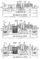
- FIGUREs 1A-F show the process steps for self aligning an emitter contact in a heterojunction bipolar transistor 10.
- the process steps that follow describe fabrication of an NPN device and can be readily adapted to fabricate a PNP device. Further, gallium arsenide is described as the primary material for each layer but other materials from Group III and Group V of the periodic table may be substituted.
- FIGURE 1A The process begins in FIGURE 1A where a subcollector layer 12 is epitaxially grown on a substrate layer 14.
- Substrate layer 14 is preferably made of semi-insulating gallium arsenide.
- Subcollector layer 12 is approximately one micron thick and doped with an N+ type conductivity having a dopant concentration of approximately 2 x 1018 cm3.
- a collector layer 16 is epitaxially grown on subcollector layer 12.
- Collector layer 16 can range in thickness from .3 to 2.0 microns and is doped with an N- conductivity type having a dopant concentration of approximately 1 x 1016 cm3.
- a base layer 18 is epitaxially grown on collector layer 16.
- Base layer 18 is approximately 1,000 Angstroms thick and doped with a P- conductivity type having a dopant concentration of greater than or equal to approximately 1 x 1018 cm3.
- base layer 18 is etched away such that no base layer material remains in the field region.
- Base layer 18 covers only a selected portion of collector layer 16.
- a dry or wet etching process may be used with slight over etching not impacting transistor operation.
- a collector implant layer 20 is patterned and implanted with an N+ conductivity type, preferably of silicon. Collector implant layer 20 may also be formed by etching down to subcollector layer 12 rather than using a silicon implant process step.
- FIGURE 1C The process continues in FIGURE 1C where an interface layer 22, preferably made of nitride or oxide, is deposited on transistor 10 in a thickness range from 400 to 3,000 Angstroms. Interface layer 22 is selectively removed from transistor 10 such that it remains only on base layer 18. Interface layer 22 is also removed to expose a portion of base layer 18. Photoresist used to pattern interface layer 22 is stripped away and transistor 10 is cleaned in preparation for the next epitaxial growth. During this cleaning process step, care must be exercised to prevent eroding away interface layer 22.
- an interface layer 22, preferably made of nitride or oxide is deposited on transistor 10 in a thickness range from 400 to 3,000 Angstroms. Interface layer 22 is selectively removed from transistor 10 such that it remains only on base layer 18. Interface layer 22 is also removed to expose a portion of base layer 18. Photoresist used to pattern interface layer 22 is stripped away and transistor 10 is cleaned in preparation for the next epitaxial growth. During this cleaning process step, care must be exercised to prevent eroding away interface layer
- an emitter layer 24 is epitaxially grown on transistor 10 such that emitter layer 24 covers collector layer 16, collector implant layer 20, and the exposed area of base layer 18.
- Emitter layer 24 is approximately 1,000 Angstroms in thickness with an N- conductivity type having a dopant concentration of approximately 2 x 1017 cm3.
- An emitter cap layer 26 is grown on emitter layer 24 and within the previously exposed area of base layer 18.
- Emitter cap layer 26 is approximately 1,000 Angstroms thick with an N+ conductivity type having a dopant concentration of approximately 2 x 1018 cm3.
- An insulating layer 28, a polycrystalline material, is deposited on interface layer 22 such that interface layer 22 is buried beneath the surface of transistor 10.
- Insulating layer 28 occurs as a result of the epitaxial growth of emitter layer 24 and emitter cap layer 26. Depending upon growth conditions, insulating layer 28 deposits onto interface layer 22 or no deposition occurs on interface layer 22. For discussion purposes, insulating layer 28 is formed to bury interface layer 22 beneath the surface of heterojunction bipolar transistor 10.
- FIGURE 1E The process continues in FIGURE 1E where high energy oxygen implants 30 isolate transistor 10 from adjacent devices by damaging the structure layers.
- a boron implant layer 32 is implanted between collector implant layer 20 and base layer 18. The damage due to the boron implant layer 32 isolates collector implant layer 20 from base layer 18 and emitter layer 24.
- Ohmic material having an N- conductivity type is deposited and selectively lifted off to form collector contact 34 and emitter contact 36.
- Emitter contact 36 can be larger than the previously exposed area of base layer 18 to avoid any misalignment problems during formation.
- Insulating layer 28 is semi-insulating and will not make good ohmic contact to emitter contact 36. Similarly, good ohmic contact is not made if no insulating layer 28 was deposited onto interface layer 22.
- the lack of a good ohmic contact to insulating layer 28 reduces leakage paths between emitter contact 36 and a subsequent base contact. Leakage paths can be further reduced by etching insulating layer 28 from beneath emitter contact 36 by using interface layer 22 as an etch stop.
- FIGURE 1F a portion of insulating layer 28 predefining a base contact is etched down to the interface layer 22 which acts as an etch stop. Interface layer 22 is then etched away to reveal base layer 18. The etch to base layer 22 is not critical as to etch time due to the etch step provided by interface layer 22. An ohmic material with a P- conductivity type is deposited and selectively lifted off to leave a base contact 38. Collector contact 34, emitter contact 36, and base contact 38 are annealed and are now ready to be probed.
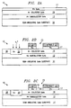
- FIGUREs 2A-C show alternative steps which may be used in the fabrication of transistor 10.
- the process beams in FIGURE 2A where a subcollector layer 12 is grown on a substrate layer 14.
- a collector layer 16 is grown on subcollector layer 12 as previously described.
- An extrinsic base layer 17 is grown on collector layer 16.
- Extrinsic base layer 17 is doped with a P+ conductivity type.
- interface layer 22 is deposited on extrinsic base layer 17.
- Interface layer 22 and extrinsic base layer 17 are selectively removed such that a gap exists within interface layer 22 and extrinsic base layer 17, exposing a portion of collector layer 16.
- Collector implant layer 20 is formed as previously described.
- Intrinsic base layer 19 forms the intrinsic base of transistor 10 while connecting to previously deposited and etched extrinsic base layer 17.
- Intrinsic base layer 19 is more lightly doped than extrinsic base layer 17 which results in higher current gains for transistor 10. Low base resistance is maintained by the heavily doped extrinsic base layer 17 grown during the initial epitaxial deposition.
- Intrinsic base layer 17 is self aligned to the subsequent emitter ohmic contact. From this point, the process continues as previously described with respect to FIGURE 1D.
- a heterojunction bipolar transistor can be fabricated to overcome misalignment problems in forming the emitter contact.
- the emitter contact region is predefined prior to forming the emitter contact such that the emitter contact is isolated from the base contact and the base layer. This isolation allows for misalignments to occur without causing a short circuit between the emitter and the base.
Landscapes
- Bipolar Transistors (AREA)
Applications Claiming Priority (2)
| Application Number | Priority Date | Filing Date | Title |
|---|---|---|---|
| US08/229,044 US5436181A (en) | 1994-04-18 | 1994-04-18 | Method of self aligning an emitter contact in a heterojunction bipolar transistor |
| US229044 | 1994-04-18 |
Publications (2)
| Publication Number | Publication Date |
|---|---|
| EP0678906A2 true EP0678906A2 (de) | 1995-10-25 |
| EP0678906A3 EP0678906A3 (de) | 1997-12-29 |
Family
ID=22859622
Family Applications (1)
| Application Number | Title | Priority Date | Filing Date |
|---|---|---|---|
| EP95105735A Withdrawn EP0678906A3 (de) | 1994-04-18 | 1995-04-18 | Verfahren zur Selbstausrichtung vom Emitter-Kontakt eines bipolaren Transistors mit Heteroübergang |
Country Status (3)
| Country | Link |
|---|---|
| US (2) | US5436181A (de) |
| EP (1) | EP0678906A3 (de) |
| JP (1) | JPH0851119A (de) |
Families Citing this family (24)
| Publication number | Priority date | Publication date | Assignee | Title |
|---|---|---|---|---|
| US5698460A (en) * | 1994-04-20 | 1997-12-16 | Texas Instruments Incorporated | Method of self-aligning an emitter contact in a planar heterojunction bipolar transistor and apparatus thereof |
| FR2764118B1 (fr) * | 1997-05-30 | 2000-08-04 | Thomson Csf | Transistor bipolaire stabilise avec elements isolants electriques |
| US6392257B1 (en) | 2000-02-10 | 2002-05-21 | Motorola Inc. | Semiconductor structure, semiconductor device, communicating device, integrated circuit, and process for fabricating the same |
| US6573599B1 (en) | 2000-05-26 | 2003-06-03 | Skyworks Solutions, Inc. | Electrical contact for compound semiconductor device and method for forming same |
| KR20030011083A (ko) | 2000-05-31 | 2003-02-06 | 모토로라 인코포레이티드 | 반도체 디바이스 및 이를 제조하기 위한 방법 |
| AU2001277001A1 (en) | 2000-07-24 | 2002-02-05 | Motorola, Inc. | Heterojunction tunneling diodes and process for fabricating same |
| US20020096683A1 (en) | 2001-01-19 | 2002-07-25 | Motorola, Inc. | Structure and method for fabricating GaN devices utilizing the formation of a compliant substrate |
| WO2002082551A1 (en) | 2001-04-02 | 2002-10-17 | Motorola, Inc. | A semiconductor structure exhibiting reduced leakage current |
| US20020158245A1 (en) * | 2001-04-26 | 2002-10-31 | Motorola, Inc. | Structure and method for fabricating semiconductor structures and devices utilizing binary metal oxide layers |
| US20030012965A1 (en) * | 2001-07-10 | 2003-01-16 | Motorola, Inc. | Structure and method for fabricating semiconductor structures and devices utilizing the formation of a compliant substrate comprising an oxygen-doped compound semiconductor layer |
| US6992321B2 (en) | 2001-07-13 | 2006-01-31 | Motorola, Inc. | Structure and method for fabricating semiconductor structures and devices utilizing piezoelectric materials |
| US7019332B2 (en) * | 2001-07-20 | 2006-03-28 | Freescale Semiconductor, Inc. | Fabrication of a wavelength locker within a semiconductor structure |
| US6855992B2 (en) | 2001-07-24 | 2005-02-15 | Motorola Inc. | Structure and method for fabricating configurable transistor devices utilizing the formation of a compliant substrate for materials used to form the same |
| US20030034491A1 (en) | 2001-08-14 | 2003-02-20 | Motorola, Inc. | Structure and method for fabricating semiconductor structures and devices for detecting an object |
| KR100388489B1 (ko) * | 2001-09-28 | 2003-06-25 | 한국전자통신연구원 | 이종접합 쌍극자 트랜지스터 및 그의 제조방법 |
| US20030071327A1 (en) | 2001-10-17 | 2003-04-17 | Motorola, Inc. | Method and apparatus utilizing monocrystalline insulator |
| US6916717B2 (en) | 2002-05-03 | 2005-07-12 | Motorola, Inc. | Method for growing a monocrystalline oxide layer and for fabricating a semiconductor device on a monocrystalline substrate |
| US20040079285A1 (en) * | 2002-10-24 | 2004-04-29 | Motorola, Inc. | Automation of oxide material growth in molecular beam epitaxy systems |
| US7169619B2 (en) | 2002-11-19 | 2007-01-30 | Freescale Semiconductor, Inc. | Method for fabricating semiconductor structures on vicinal substrates using a low temperature, low pressure, alkaline earth metal-rich process |
| US6885065B2 (en) * | 2002-11-20 | 2005-04-26 | Freescale Semiconductor, Inc. | Ferromagnetic semiconductor structure and method for forming the same |
| US6963090B2 (en) * | 2003-01-09 | 2005-11-08 | Freescale Semiconductor, Inc. | Enhancement mode metal-oxide-semiconductor field effect transistor |
| US7020374B2 (en) | 2003-02-03 | 2006-03-28 | Freescale Semiconductor, Inc. | Optical waveguide structure and method for fabricating the same |
| US6965128B2 (en) | 2003-02-03 | 2005-11-15 | Freescale Semiconductor, Inc. | Structure and method for fabricating semiconductor microresonator devices |
| JPWO2021214866A1 (de) * | 2020-04-21 | 2021-10-28 |
Family Cites Families (13)
| Publication number | Priority date | Publication date | Assignee | Title |
|---|---|---|---|---|
| EP0240307B1 (de) * | 1986-04-01 | 1993-12-22 | Matsushita Electric Industrial Co., Ltd. | Bipolarer Transistor und sein Herstellungsverfahren |
| JPH0797589B2 (ja) * | 1986-06-26 | 1995-10-18 | ソニー株式会社 | ヘテロ接合型バイポ−ラトランジスタの製造方法 |
| JP2743377B2 (ja) * | 1987-05-20 | 1998-04-22 | 日本電気株式会社 | 半導体薄膜の製造方法 |
| US5064772A (en) * | 1988-08-31 | 1991-11-12 | International Business Machines Corporation | Bipolar transistor integrated circuit technology |
| US4954457A (en) * | 1988-10-31 | 1990-09-04 | International Business Machines Corporation | Method of making heterojunction bipolar transistors |
| US4935797A (en) * | 1988-10-31 | 1990-06-19 | International Business Machines Corporation | Heterojunction bipolar transistors |
| US5098853A (en) * | 1988-11-02 | 1992-03-24 | Hughes Aircraft Company | Self-aligned, planar heterojunction bipolar transistor and method of forming the same |
| US5068756A (en) * | 1989-02-16 | 1991-11-26 | Texas Instruments Incorporated | Integrated circuit composed of group III-V compound field effect and bipolar semiconductors |
| GB2228617A (en) * | 1989-02-27 | 1990-08-29 | Philips Electronic Associated | A method of manufacturing a semiconductor device having a mesa structure |
| EP0436753B1 (de) * | 1990-01-08 | 1994-05-25 | Siemens Aktiengesellschaft | Verfahren zur Herstellung eines selbstjustierten Emitter-Basis-Komplexes |
| US5077231A (en) * | 1991-03-15 | 1991-12-31 | Texas Instruments Incorporated | Method to integrate HBTs and FETs |
| JP2855908B2 (ja) * | 1991-09-05 | 1999-02-10 | 日本電気株式会社 | 半導体装置及びその製造方法 |
| US5272095A (en) * | 1992-03-18 | 1993-12-21 | Research Triangle Institute | Method of manufacturing heterojunction transistors with self-aligned metal contacts |
-
1994
- 1994-04-18 US US08/229,044 patent/US5436181A/en not_active Expired - Lifetime
-
1995
- 1995-04-17 JP JP7090992A patent/JPH0851119A/ja active Pending
- 1995-04-18 EP EP95105735A patent/EP0678906A3/de not_active Withdrawn
- 1995-05-16 US US08/441,847 patent/US5548141A/en not_active Expired - Lifetime
Also Published As
| Publication number | Publication date |
|---|---|
| JPH0851119A (ja) | 1996-02-20 |
| US5548141A (en) | 1996-08-20 |
| EP0678906A3 (de) | 1997-12-29 |
| US5436181A (en) | 1995-07-25 |
Similar Documents
| Publication | Publication Date | Title |
|---|---|---|
| US5436181A (en) | Method of self aligning an emitter contact in a heterojunction bipolar transistor | |
| US5583059A (en) | Fabrication of vertical SiGe base HBT with lateral collector contact on thin SOI | |
| US5407842A (en) | Enhanced performance bipolar transistor process | |
| EP0483487B1 (de) | Transistor mit selbstjustierender epitaxialer Basis und dessen Herstellungsverfahren | |
| US4731340A (en) | Dual lift-off self aligning process for making heterojunction bipolar transistors | |
| EP0729177A2 (de) | Bipolarer Transistor | |
| US5118634A (en) | Self-aligned integrated circuit bipolar transistor having monocrystalline contacts | |
| US4593457A (en) | Method for making gallium arsenide NPN transistor with self-aligned base enhancement to emitter region and metal contact | |
| JPH0744232B2 (ja) | Bi―CMOSデバイス製造方法 | |
| JPH09102504A (ja) | 自己整列サブミクロンヘテロ接合バイポーラトランジスタおよびその製造方法 | |
| US4997775A (en) | Method for forming a complementary bipolar transistor structure including a self-aligned vertical PNP transistor | |
| US5097312A (en) | Heterojunction bipolar transistor and integration of same with field effect device | |
| US5344786A (en) | Method of fabricating self-aligned heterojunction bipolar transistors | |
| US5434091A (en) | Method for making collector up bipolar transistors having reducing junction capacitance and increasing current gain | |
| US20030107051A1 (en) | Super self -aligned heterojunction biplar transistor and its manufacturing method | |
| US5716859A (en) | Method of fabricating a silicon BJT | |
| US6271097B1 (en) | Method of fabricating a low base-resistance bipolar transistor | |
| US5286997A (en) | Method for forming an isolated, low resistance epitaxial subcollector for bipolar transistors | |
| US5946582A (en) | Method of making an InP-based heterojunction bipolar transistor with reduced base-collector capacitance | |
| EP0605920B1 (de) | Kaskodenschaltungsstruktur mit bipolaren Epitoxial-Transistoren und niedrig gelegenem Basisanschluss | |
| EP0671762A2 (de) | Verringerung der Störkapazität der Basis-Kollektor-Verbindung von bipolaren heterojunktiven Transistoren | |
| EP0375323A1 (de) | Ein vertikaler Hochleistungs-Bipolartransistor, Kompatibel mit einer hochwertigen ECL-Bipolar-Technologie und dessen Herstellungsverfahren | |
| US5420052A (en) | Method of fabricating a semiplanar heterojunction bipolar transistor | |
| EP0272280B1 (de) | Verfahren zur herstellung eines iii-v-halbleiterbauelementes | |
| US5698460A (en) | Method of self-aligning an emitter contact in a planar heterojunction bipolar transistor and apparatus thereof |
Legal Events
| Date | Code | Title | Description |
|---|---|---|---|
| PUAI | Public reference made under article 153(3) epc to a published international application that has entered the european phase |
Free format text: ORIGINAL CODE: 0009012 |
|
| AK | Designated contracting states |
Kind code of ref document: A2 Designated state(s): DE FR GB IT NL |
|
| PUAL | Search report despatched |
Free format text: ORIGINAL CODE: 0009013 |
|
| AK | Designated contracting states |
Kind code of ref document: A3 Designated state(s): DE FR GB IT NL |
|
| REG | Reference to a national code |
Ref country code: IE Ref legal event code: FG4D Free format text: 79919 |
|
| STAA | Information on the status of an ep patent application or granted ep patent |
Free format text: STATUS: THE APPLICATION IS DEEMED TO BE WITHDRAWN |
|
| 18D | Application deemed to be withdrawn |
Effective date: 19980630 |