EP0680144B1 - Empfängeranordnung - Google Patents
Empfängeranordnung Download PDFInfo
- Publication number
- EP0680144B1 EP0680144B1 EP95302256A EP95302256A EP0680144B1 EP 0680144 B1 EP0680144 B1 EP 0680144B1 EP 95302256 A EP95302256 A EP 95302256A EP 95302256 A EP95302256 A EP 95302256A EP 0680144 B1 EP0680144 B1 EP 0680144B1
- Authority
- EP
- European Patent Office
- Prior art keywords
- pulse
- stage
- voltage
- receiver
- output signal
- Prior art date
- Legal status (The legal status is an assumption and is not a legal conclusion. Google has not performed a legal analysis and makes no representation as to the accuracy of the status listed.)
- Expired - Lifetime
Links
- 230000035945 sensitivity Effects 0.000 claims abstract description 4
- 230000004044 response Effects 0.000 claims description 5
- 239000003990 capacitor Substances 0.000 description 14
- 238000001514 detection method Methods 0.000 description 6
- 238000010586 diagram Methods 0.000 description 3
- 230000000694 effects Effects 0.000 description 3
- 230000009471 action Effects 0.000 description 2
- 230000008901 benefit Effects 0.000 description 2
- 230000008859 change Effects 0.000 description 2
- 230000007423 decrease Effects 0.000 description 2
- 230000010354 integration Effects 0.000 description 2
- 238000000034 method Methods 0.000 description 2
- 230000008569 process Effects 0.000 description 2
- XUIMIQQOPSSXEZ-UHFFFAOYSA-N Silicon Chemical compound [Si] XUIMIQQOPSSXEZ-UHFFFAOYSA-N 0.000 description 1
- 230000003321 amplification Effects 0.000 description 1
- 230000007850 degeneration Effects 0.000 description 1
- 230000001419 dependent effect Effects 0.000 description 1
- 238000001914 filtration Methods 0.000 description 1
- 238000003199 nucleic acid amplification method Methods 0.000 description 1
- 230000003071 parasitic effect Effects 0.000 description 1
- 230000005855 radiation Effects 0.000 description 1
- 229910052710 silicon Inorganic materials 0.000 description 1
- 239000010703 silicon Substances 0.000 description 1
Images


Classifications
-
- H—ELECTRICITY
- H04—ELECTRIC COMMUNICATION TECHNIQUE
- H04B—TRANSMISSION
- H04B10/00—Transmission systems employing electromagnetic waves other than radio-waves, e.g. infrared, visible or ultraviolet light, or employing corpuscular radiation, e.g. quantum communication
- H04B10/11—Arrangements specific to free-space transmission, i.e. transmission through air or vacuum
- H04B10/114—Indoor or close-range type systems
-
- H—ELECTRICITY
- H03—ELECTRONIC CIRCUITRY
- H03K—PULSE TECHNIQUE
- H03K5/00—Manipulating of pulses not covered by one of the other main groups of this subclass
- H03K5/01—Shaping pulses
- H03K5/08—Shaping pulses by limiting; by thresholding; by slicing, i.e. combined limiting and thresholding
- H03K5/082—Shaping pulses by limiting; by thresholding; by slicing, i.e. combined limiting and thresholding with an adaptive threshold
Definitions
- the invention concerns a receiver arrangement for use in a remote-control system, and in particular, but not exclusively, a receiver arrangement for use in an infrared pulse position modulation (PPM) remote-control system.
- PPM pulse position modulation
- Infrared remote-control systems are known in which an infrared diode is used in conjunction with appropriate circuitry in a receiver to pick up and demodulate data pulses transmitted from an infrared transmitting diode situated at a point remote from the receiver.
- EP 0 564 349 discloses a remote-control receiver for a vehicle comprising an opto-electrical transducer connected to an amplifier. An integrator is connected to the. amplifier output and provides a signal which is subtracted from the transducer signal so as to eliminate low frequency parasitic signals from the transducer signal.
- FIG. 1 Another known form of a receiver front-end stage is shown in Figure 1.
- the stage centres around a bipolar transistor 12 arranged to receive the current output from an infrared diode 19.
- a resistor 13 is connected between the base and collector of the transistor 12
- a capacitor 14 is connected between the base and a first reference potential 15, and a resistor 16 is connected between the same reference potential and the emitter of the transistor 12.
- a current source 17 is connected between a second reference potential 18 and the collector of the transistor 12, and the infrared diode 19 is connected in parallel with the current source 17.
- a diode 20 may also be interposed between the current source 17 and the collector of the transistor 12, for reasons which will be explained below.
- a diode 20 may be added as shown to lift the output voltage of the circuit to a level which can more easily be dealt with by subsequent circuitry.
- a disadvantage of known receiver arrangements using the above circuit is that, since the positive-going pulse appearing on the collector is fast and can also be of large amplitude, any subsequent circuitry used to detect and decode the received pulse has to exhibit a high bandwidth to cope with this.
- High-bandwidth amplifying and other devices require high supply currents to operate effectively, and where such an arrangement is incorporated in a portable, battery-operated unit, which is often the case, the drain on the battery can be considerable.
- a receiver arrangement for use in a remote-control system, comprising a receiver stage for receiving a current pulse from a transducer and for outputting a voltage output signal in response to the current pulse, and a pulse detector stage for receiving the voltage outpur signal of the receiver stage and for providing a data output signal in dependence thereon
- the receiver stage may comprising an amplifying element having first and second output terminals and an input terminal, the first and second output terminals being connected respectively to a transducer input node and to a first reference potential, the input terminal being connected to the first output terminal through a first resistance and to the first reference potential through a first capacitance, the output of the receiver stage being taken from the transducer input node whereby the voltage output signal comprises a first pulse substantially coincident with the received current pulse and a second, immediately following, opposite-going pulse at the end of the received current pulse having a pulses width greater than that of the first pulse, characterised in that the pulse detector stage is arranged to provide
- the second pulse is easier to detect, as it directly follows a disturbance known to be in the opposite direction. The result is an increased receiver sensitivity.
- the receiver stage may be arranged to limit the amplitude of the second pulse. Such limiting prevents overloading of the receiver stage during high input signal conditions.
- the second output terminal may be connected to the first reference potential through a second resistance, which has the advantage of helping to stabilise the operating conditions of the amplifying element.
- a voltage-shifter may be advantageously interposed between the first output terminal of the amplifying element and the transducer input node. This lifts the quiescent output voltage level of the receiver stage and facilitates the subsequent pulse detection process.
- a transducer may be connected between the transducer input node and a second reference potential.
- the amplifying element is preferably a bipolar transistor.
- the detector stage may include a pulse discriminator stage, for forming a first output signal representative of the average level of the output signal of the receiver stage and a second output signal representative of the instantaneous level of the output signal of the receiver stage, and a comparator stage for comparing the first and second output signals of the pulse detector stage and providing, on the basis of that comparison, the data output signal.
- a pulse discriminator stage for forming a first output signal representative of the average level of the output signal of the receiver stage and a second output signal representative of the instantaneous level of the output signal of the receiver stage
- a comparator stage for comparing the first and second output signals of the pulse detector stage and providing, on the basis of that comparison, the data output signal.
- the pulse discriminator stage may include first and second voltage followers for providing the first and second output signals of the pulse discriminator stage, the first and second voltage-followers being arranged to be commonly supplied with a signal representative of the output signal of the receiver stage, and the first voltage-follower being arranged to provide the first output signal of the pulse discriminator stage through a low-pass filter.
- the filter preferably includes a third resistance and a second capacitance connected in series between the output of the first voltage follower and a reference potential.
- two different signals may be derived from the pulse discriminator stage, the difference of which signals represents the pulse component of the receiver stage output signal. Any quiescent component of that output signal, representing largely the ambient light level experienced by the transducer, is common-mode as far as the voltage followers are concerned.
- a fourth resistance may be connected in parallel with the second capacitance, the fourth resistance serving to adjust the sensitivity of the receiver arrangement.
- a second voltage shifter may be interposed between the receiver stage and the first and second voltage followers of the pulse discriminator stage.
- the second voltage shifter may include a third voltage follower feeding the first and second voltage followers.
- At least one diode element may be interposed between the third voltage follower and the first and second voltage followers.
- a current source may be included in the output circuit of each voltage follower, establishing an output current in each follower.
- the voltage followers are preferably emitter followers.
- the amplifying element and the first and second voltage followers may be transistors of one polarity type, while the third voltage follower may be a transistor of the opposite polarity type.
- a buffer stage may be interposed between the receiver stage and the pulse detector stage.
- the buffer stage may be arranged to amplify the output signal of the receiver stage.
- a remote control apparatus characterised by a receiver arrangement, as described above, and an infrared transducer connected thereto.
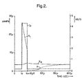
- the collector voltage V C rises instantaneously from its quiescent value of approximately 0.55V to 0.55 + (25 ⁇ A ⁇ 160 K) ⁇ 4.5V, upon which it decreases rapidly as the share of I P flowing through resistor 13 is progressively diverted into the collector of transistor 12 due to the increase of charge on capacitor 14.
- the collector load is the resistor 13 fed from the voltage on the capacitor 14 at the moment the input current pulse ends.
- the pulse decays as the capacitor 14 slowly discharges through resistor 13 (see the part of the V C curve marked "X" and the corresponding part of the curve of capacitor voltage (V 14 ) in Figure 2). This causes some stretching of the pulse which can facilitate detection of the pulse in a subsequent pulse detection stage.
- the transistor At high levels of diode pulse current the transistor will saturate, giving a maximum pulse amplitude of slightly under 0.6 V and considerable stretching of the pulse.
- an amplifier/buffer 30 receives the output voltage signal from the receiver stage shown in Figure 1 and amplifies an AC component of that output signal by a set amount, while subjecting a DC component, corresponding mainly to the ambient light level of the diode 19's environment, to unity-gain amplification only. This minimises the effects of ambient radiation on the pulse detection circuitry, while boosting the desired pulse signal component of the receiver stage output.
- the output of the amplifier/buffer 30 is taken to a pulse detector stage 40, consisting of an emitter follower stage 41, two parallel-driven emitter follower stages 42, 43 and associated current sources 44, 45, 46 and a low-pass filter 47.
- Emitter follower 41 comprises a PNP transistor 48, a voltage shifter 49, consisting of three series-connected diodes, and the current source 44.
- the base of transistor 48 is fed from the output of the amplifier/buffer 30, while the collector of the transistor 48 is taken to a reference potential 15 and the emitter is taken to a positive supply rail 51 by way of the voltage shifter 49 and the current source 44.
- the voltage shifter lifts the low quiescent input voltage present on the base of the transistor 48 to a level more suitable for following circuitry.
- the junction of the voltage shifter 49 and the current source 44 is taken to the commoned bases of NPN transistors 52 and 53, which, together with current sources 45 and 46, respectively, form the emitter followers 42 and 43.
- the collectors of transistors 52, 53 are taken to the positive supply rail 51, while the emitters of these transistors are taken to their respective current sources 45, 46, in the case of follower 42 via a resistor 54.
- Resistor 54 forms one half of the low-pass filter 47, the other half being constituted by the parallel combination of a capacitor 55 and a resistor 56.
- Resistor 56 and capacitor 55 are connected across the current source 45.
- the quiescent output of the amplifier/buffer 30 is effectively shifted in potential to the potential existing on the emitters of transistors 52 and 53.
- a potential difference is set up between points "A" and "B” in Figure 4 due to the current flowing through the resistor 54 and the range-setting resistor 56.
- resistor 56 may be omitted or else made very high impedance, e.g. 3 M ⁇ .
- the signals on the points "A" and “B” of the pulse detector stage 40 are taken to the inputs of a comparator stage 60 based around a comparator 61. Under no-signal conditions, input 62 of comparator 61 is at a higher voltage than input 63 and consequently the data output 64 of the comparator 61 is held low.
- the emitter follower 43 When a diode pulse signal from the receiver stage is received on the input of the amplifier 30, the emitter follower 43 provides on its emitter a faithful reproduction of that signal, i.e. the voltage V C shown in Figure 2, whereas the emitter follower 42 provides at the junction of the resistor 54 and the current source 45 the average of that signal. This is due to the action of the filter comprised principally of the resistor 54 and the capacitor 55.
- the collector voltage V C responds to the incident, transmitted data pulse by going high for a time duration corresponding to the duration of the received pulse. This same positive-going pulse is reproduced at point "B", but not at point "A" due to the filtering action of the filter 47.
- the already existing potential difference between points "A" and "B” is increased and the output 64 of the comparator 61 continues to be held low.
- V C drops suddenly and goes negative (see Figure 2).
- the negative excursion of V C will be sufficient to change the output state of the comparator 61 and a data output pulse will be sent out to a following decoder stage (not shown).
Landscapes
- Physics & Mathematics (AREA)
- Electromagnetism (AREA)
- Engineering & Computer Science (AREA)
- Computer Networks & Wireless Communication (AREA)
- Signal Processing (AREA)
- Nonlinear Science (AREA)
- Structure Of Receivers (AREA)
- Input Circuits Of Receivers And Coupling Of Receivers And Audio Equipment (AREA)
- Ultra Sonic Daignosis Equipment (AREA)
- Amplifiers (AREA)
- Selective Calling Equipment (AREA)
- Circuits Of Receivers In General (AREA)
Claims (17)
- Empfängeranordnung zur Verwendung in einem Fernsteuerungssystem mit einer Empfängerstufe zum Empfangen eines Stromimpulses von einem Wandler (19) und zum Ausgeben eines Spannungsausgangssignals als Antwort auf den Stromimpuls, und einer Impulsdetektorstufe (40) zum Empfangen des Spannungsausgangssignals der Empfängerstufe und zum Liefern eines Datenausgangssignals (64) in Abhängigkeit davon, wobei die Empfängerstufe ein Verstärkungselement (12) mit einem ersten und einem zweiten Ausgangsanschluß und einem Eingangsanschluß aufweist, der erste und der zweite Ausgangsanschluß mit einem Eingangsknoten des Wandlers bzw. mit einem ersten Referenzpotential (15) verbunden sind, der Eingangsanschluß mit dem ersten Ausgangsanschluß über einen ersten Widerstand (13) und mit dem ersten Referenzpotential (15) über eine erste Kapazität (14) verbunden ist, das Ausgangssignal der Empfängerstufe vom Eingangsknoten des Wandlers abgenommen wird, wodurch das Spannungsausgangssignal einen ersten Impuls, der im wesentlichen mit dem empfangenen Stromimpuls übereinstimmt, und einen zweiten, unmittelbar folgenden, entgegengesetzten Impuls am Ende des empfangenen Stromimpulses aufweist, der eine Impulsbreite hat, die größer ist als die des ersten Impulses, dadurch gekennzeichnet, daß die Impulsdetektorstufe (40) so eingerichtet ist, daß sie das Datenausgangssignal als Antwort auf den zweiten Impuls liefert.
- Empfängeranordnung nach Anspruch 1, dadurch gekennzeichnet, daß die Empfängerstufe so eingerichtet ist, daß die Amplitude des zweiten Impulses begrenzt wird.
- Empfängeranordnung nach Anspruch 1 oder 2, dadurch gekennzeichnet, daß der zweite Ausgangsanschluß mit dem ersten Referenzpotential (15) über einen zweiten Widerstand (16) verbunden ist.
- Empfängeranordnung nach einem der vorhergehenden Ansprüche, gekennzeichnet durch einen ersten Spannungsangleicher (20), der zwischen den ersten Ausgangsanschluß des Verstärkungselements (12) und den Eingangsknoten des Wandlers geschaltet ist.
- Empfängeranordnung nach einem der vorhergehenden Ansprüche, gekennzeichnet durch einen Wandler (19), der zwischen den Eingangsknoten des Wandlers und ein zweites Referenzpotential (18) geschaltet ist.
- Empfängeranordnung nach einem der vorhergehenden Ansprüche, dadurch gekennzeichnet, daß das Verstärkungselement ein bipolarer Transistor (12) ist.
- Empfängeranordnung nach einem der vorhergehenden Ansprüche, dadurch gekennzeichnet, daß die Impulsdetektorstufe (40) aufweist: eine Impulsdiskriminatorstufe (42, 43) zur Bildung eines ersten Ausgangssignals (A), das den durchschnittlichen Pegel des Ausgangssignals der Empfängerstufe darstellt, und eines zweiten Ausgangssignals (B), das den Momentanpegel des Ausgangssignals der Empfängerstufe darstellt, und eine Komparatorstufe (60) zum Vergleichen des ersten und zweiten Ausgangssignals der Impulsdetektorstufe und Liefern des Datenausgangssignals auf der Grundlage dieses Vergleichs.
- Empfängeranordnung nach Anspruch 7, dadurch gekennzeichnet, daß die Impulsdiskriminatorstufe (42, 43) einen ersten und einen zweiten Spannungsfolger (52, 53) zum Liefern des ersten und zweiten Ausgangssignals (A, B) der Impulsdiskriminatorstufe (42, 43) aufweist, wobei der erste und zweite Spannungsfolger (52, 53) so eingerichtet sind, daß sie gemeinsam mit einem Signal versorgt werden, das das Ausgangssignal der Empfängerstufe darstellt, und der erste Spannungsfolger (52) so eingerichtet ist, daß er das erste Ausgangssignal (A) der Impulsdiskriminatorstufe (42, 43) über ein Tiefpaßfilter (47) liefert.
- Empfängeranordnung nach Anspruch 8, dadurch gekennzeichnet, daß das Tiefpaßfilter (47) einen dritten Widerstand (54) und eine zweite Kapazität (55) aufweist, die zwischen den Ausgang des ersten Spannungsfolgers (52) und ein Referenzpotential (15) in Reihe geschaltet sind.
- Empfängeranordnung nach Anspruch 9, gekennzeichnet durch einen vierten Widerstand (56), der mit der zweiten Kapazität (55) parallelgeschaltet ist, wobei der vierte Widerstand (56) dazu dient, die Empfindlichkeit der Empfängeranordnung einzustellen.
- Empfängeranordnung nach einem der Ansprüche 8 bis 10, gekennzeichnet durch einen zweiten Spannungsangleicher (41), der zwischen die Empfängerstufe und den ersten und zweiten Spannungsfolger (52, 53) der Impulsdiskriminatorstufe (42, 43) geschaltet ist.
- Empfängeranordnung nach Anspruch 11, dadurch gekennzeichnet, daß der zweite Spannungsangleicher (41) einen dritten Spannungsfolger (48) aufweist, die den ersten und zweiten Spannungsfolger (52, 53) versorgt.
- Empfängeranordnung nach Anspruch 12, gekennzeichnet durch mindestens ein Diodenelement (49), das zwischen den dritten Spannungsfolger (48) und den ersten und zweiten Spannungsfolger (52, 53) geschaltet ist.
- Empfängeranordnung nach einem der Ansprüche 8 bis 13, gekennzeichnet durch eine Stromquelle (44-46) in der Ausgangsschaltung jedes Spannungsfolgers (48, 52, 53).
- Empfängeranordnung nach einem der Ansprüche 8 bis 14, dadurch gekennzeichnet, daß die Spannungsfolger (48, 52, 53) Emitterfolger sind.
- Empfängeranordnung nach Anspruch 6, 12 und 15, dadurch gekennzeichnet, daß das Verstärkungselement (12) und der erste und zweite Spannungsfolger (52, 53) Transistoren einer Polaritätsart sind, wogegen der dritte Spannungsfolger (48) ein Transistor der entgegengesetzten Polaritätsart ist.
- Fernsteuerungsvorrichtung, gekennzeichnet durch eine Empfängeranordnung nach einem der vorhergehenden Ansprüche und einen mit dieser verbundenen Infrarotwandler.
Applications Claiming Priority (2)
| Application Number | Priority Date | Filing Date | Title |
|---|---|---|---|
| GB9408576A GB2289177B (en) | 1994-04-29 | 1994-04-29 | Receiver arrangement |
| GB9408576 | 1994-04-29 |
Publications (2)
| Publication Number | Publication Date |
|---|---|
| EP0680144A1 EP0680144A1 (de) | 1995-11-02 |
| EP0680144B1 true EP0680144B1 (de) | 2002-03-06 |
Family
ID=10754360
Family Applications (1)
| Application Number | Title | Priority Date | Filing Date |
|---|---|---|---|
| EP95302256A Expired - Lifetime EP0680144B1 (de) | 1994-04-29 | 1995-04-04 | Empfängeranordnung |
Country Status (6)
| Country | Link |
|---|---|
| US (1) | US5661754A (de) |
| EP (1) | EP0680144B1 (de) |
| JP (1) | JPH07303051A (de) |
| AT (1) | ATE214209T1 (de) |
| DE (1) | DE69525677T2 (de) |
| GB (1) | GB2289177B (de) |
Families Citing this family (5)
| Publication number | Priority date | Publication date | Assignee | Title |
|---|---|---|---|---|
| IL128944A (en) * | 1996-09-20 | 2003-01-12 | Tadao Ohnaka | Multiple signal processing unit for utility wiring by receiver/lan and utility wiring system by receiver/lan |
| JP3350376B2 (ja) * | 1996-11-25 | 2002-11-25 | シャープ株式会社 | 波形整形回路およびそれを用いる赤外線データ通信装置 |
| JP3364154B2 (ja) * | 1998-05-22 | 2003-01-08 | 三菱電機株式会社 | 感熱式流量計 |
| JP2006513626A (ja) | 2003-01-14 | 2006-04-20 | コーニンクレッカ フィリップス エレクトロニクス エヌ ヴィ | フォトダイオードを有するリモートコントロール受信機のための回路配置および配置方法 |
| JP5185354B2 (ja) * | 2010-11-26 | 2013-04-17 | リズム時計工業株式会社 | 光学モーションセンサー |
Family Cites Families (13)
| Publication number | Priority date | Publication date | Assignee | Title |
|---|---|---|---|---|
| GB386743A (en) * | 1931-11-12 | 1933-01-26 | Siemens Brothers & Co Ltd | Improvements in telegraphy and like signalling systems |
| DE1280277B (de) * | 1965-04-30 | 1968-10-17 | Siemens Ag | Schaltungsanordnung zum abwechselnden Anschalten der Pole einer Spannungsquelle an einen Verbraucher, insbesondere Einfachstrom-Doppelstrom-Telegrafierzeichenumsetzer |
| DE1512549A1 (de) * | 1967-04-05 | 1969-05-14 | Standard Elek K Lorenz Ag | Schaltung zur Umwandlung reckteckfoermiger Impulse |
| US3729633A (en) * | 1970-11-24 | 1973-04-24 | Ibm | Optical receiver having a maximized signal-to-noise ratio |
| GB1379061A (en) * | 1972-07-18 | 1975-01-02 | Geraetewerk Karl Marx Stadt Im | Citcuit arrangement for use in telegraph apparatus for the conver sion of single current signals into double current signals |
| US3916326A (en) * | 1974-01-31 | 1975-10-28 | Reliance Electric Co | Sensing circuit including polarity discriminator |
| US4206316A (en) * | 1976-05-24 | 1980-06-03 | Hughes Aircraft Company | Transmitter-receiver system utilizing pulse position modulation and pulse compression |
| US4153848A (en) * | 1976-07-07 | 1979-05-08 | Ohkura Electric Co. Ltd. | Receiver circuit |
| JPH0770975B2 (ja) * | 1988-01-26 | 1995-07-31 | シャープ株式会社 | 波形変換回路 |
| DE4011539A1 (de) * | 1990-04-10 | 1991-10-17 | Standard Elektrik Lorenz Ag | Vorrichtung zum empfang optischer signale |
| FR2689666A1 (fr) * | 1992-04-03 | 1993-10-08 | Peugeot | Dispositif de réception d'un signal optique, notamment pour véhicule automobile. |
| JP2845253B2 (ja) * | 1992-07-15 | 1999-01-13 | 日本電気株式会社 | キードパルス検出回路 |
| JP2625347B2 (ja) * | 1993-04-20 | 1997-07-02 | 日本電気株式会社 | ディジタル受信器の自動オフセット制御回路 |
-
1994
- 1994-04-29 GB GB9408576A patent/GB2289177B/en not_active Revoked
-
1995
- 1995-03-28 US US08/411,539 patent/US5661754A/en not_active Expired - Fee Related
- 1995-04-04 DE DE69525677T patent/DE69525677T2/de not_active Expired - Fee Related
- 1995-04-04 AT AT95302256T patent/ATE214209T1/de not_active IP Right Cessation
- 1995-04-04 EP EP95302256A patent/EP0680144B1/de not_active Expired - Lifetime
- 1995-04-18 JP JP7115322A patent/JPH07303051A/ja not_active Withdrawn
Also Published As
| Publication number | Publication date |
|---|---|
| EP0680144A1 (de) | 1995-11-02 |
| GB2289177A (en) | 1995-11-08 |
| US5661754A (en) | 1997-08-26 |
| GB2289177B (en) | 1998-04-15 |
| JPH07303051A (ja) | 1995-11-14 |
| DE69525677D1 (de) | 2002-04-11 |
| GB9408576D0 (en) | 1994-06-22 |
| DE69525677T2 (de) | 2002-09-12 |
| ATE214209T1 (de) | 2002-03-15 |
Similar Documents
| Publication | Publication Date | Title |
|---|---|---|
| US5798664A (en) | Offset cancelling amplifier circuit having Miller integrator as offset detector | |
| AU671003B2 (en) | Automatic offset control circuit for digital receiver | |
| EP1011194B1 (de) | Schneller optoelektronischer Differenz-Empfänger | |
| CN1007031B (zh) | 光接收器 | |
| JPH02501612A (ja) | 光学式受信器の入力段におけるダイナミックレンジを増大させる方法及び構成 | |
| US5498993A (en) | Pulse light-receiving circuit with means to minimize power source noise | |
| US20050133691A1 (en) | Optical receiver circuit | |
| US6956439B1 (en) | Transimpedance amplifier with controllable noise reduction | |
| EP0680144B1 (de) | Empfängeranordnung | |
| CN100559704C (zh) | 光接收用前置放大器 | |
| US4817208A (en) | Fiber optic receiver | |
| US20080101802A1 (en) | Receiving Apparatus and Electronic Device Using the Same | |
| JPH01286655A (ja) | 光受信回路 | |
| JPH11284444A (ja) | プリアンプ回路およびプリアンプ方法 | |
| JP3537560B2 (ja) | 電流−電圧変換器及び光受信器 | |
| JP3487893B2 (ja) | 光パルス受信回路 | |
| JP2543612B2 (ja) | 受光装置 | |
| US4904860A (en) | Optical signal detection circuit with constant current sources | |
| US6765420B2 (en) | Pulse width detection circuit filtering the input signal and generating a binary signal | |
| JP2001168374A (ja) | 光電気変換回路 | |
| JP2546912B2 (ja) | 交流増幅器 | |
| JP3039875B2 (ja) | 光受信器 | |
| JPS61237534A (ja) | 光受信回路 | |
| GB2205209A (en) | Wideband post-amplifier particularly for a product detector in a demodulator | |
| JPH10209825A (ja) | しきい値制御回路 |
Legal Events
| Date | Code | Title | Description |
|---|---|---|---|
| PUAI | Public reference made under article 153(3) epc to a published international application that has entered the european phase |
Free format text: ORIGINAL CODE: 0009012 |
|
| AK | Designated contracting states |
Kind code of ref document: A1 Designated state(s): AT DE ES FR GB IT |
|
| 17P | Request for examination filed |
Effective date: 19960423 |
|
| RAP1 | Party data changed (applicant data changed or rights of an application transferred) |
Owner name: MITEL SEMICONDUCTOR LIMITED |
|
| 17Q | First examination report despatched |
Effective date: 19990817 |
|
| GRAG | Despatch of communication of intention to grant |
Free format text: ORIGINAL CODE: EPIDOS AGRA |
|
| GRAG | Despatch of communication of intention to grant |
Free format text: ORIGINAL CODE: EPIDOS AGRA |
|
| GRAH | Despatch of communication of intention to grant a patent |
Free format text: ORIGINAL CODE: EPIDOS IGRA |
|
| GRAH | Despatch of communication of intention to grant a patent |
Free format text: ORIGINAL CODE: EPIDOS IGRA |
|
| REG | Reference to a national code |
Ref country code: GB Ref legal event code: IF02 |
|
| GRAA | (expected) grant |
Free format text: ORIGINAL CODE: 0009210 |
|
| AK | Designated contracting states |
Kind code of ref document: B1 Designated state(s): AT DE ES FR GB IT |
|
| PG25 | Lapsed in a contracting state [announced via postgrant information from national office to epo] |
Ref country code: IT Free format text: LAPSE BECAUSE OF FAILURE TO SUBMIT A TRANSLATION OF THE DESCRIPTION OR TO PAY THE FEE WITHIN THE PRESCRIBED TIME-LIMIT;WARNING: LAPSES OF ITALIAN PATENTS WITH EFFECTIVE DATE BEFORE 2007 MAY HAVE OCCURRED AT ANY TIME BEFORE 2007. THE CORRECT EFFECTIVE DATE MAY BE DIFFERENT FROM THE ONE RECORDED. Effective date: 20020306 Ref country code: AT Free format text: LAPSE BECAUSE OF FAILURE TO SUBMIT A TRANSLATION OF THE DESCRIPTION OR TO PAY THE FEE WITHIN THE PRESCRIBED TIME-LIMIT Effective date: 20020306 |
|
| REF | Corresponds to: |
Ref document number: 214209 Country of ref document: AT Date of ref document: 20020315 Kind code of ref document: T |
|
| PGFP | Annual fee paid to national office [announced via postgrant information from national office to epo] |
Ref country code: GB Payment date: 20020404 Year of fee payment: 8 |
|
| PGFP | Annual fee paid to national office [announced via postgrant information from national office to epo] |
Ref country code: FR Payment date: 20020410 Year of fee payment: 8 Ref country code: DE Payment date: 20020410 Year of fee payment: 8 |
|
| REF | Corresponds to: |
Ref document number: 69525677 Country of ref document: DE Date of ref document: 20020411 |
|
| ET | Fr: translation filed | ||
| PG25 | Lapsed in a contracting state [announced via postgrant information from national office to epo] |
Ref country code: ES Free format text: LAPSE BECAUSE OF FAILURE TO SUBMIT A TRANSLATION OF THE DESCRIPTION OR TO PAY THE FEE WITHIN THE PRESCRIBED TIME-LIMIT Effective date: 20020925 |
|
| PLBE | No opposition filed within time limit |
Free format text: ORIGINAL CODE: 0009261 |
|
| STAA | Information on the status of an ep patent application or granted ep patent |
Free format text: STATUS: NO OPPOSITION FILED WITHIN TIME LIMIT |
|
| 26N | No opposition filed |
Effective date: 20021209 |
|
| PG25 | Lapsed in a contracting state [announced via postgrant information from national office to epo] |
Ref country code: GB Free format text: LAPSE BECAUSE OF NON-PAYMENT OF DUE FEES Effective date: 20030404 |
|
| PG25 | Lapsed in a contracting state [announced via postgrant information from national office to epo] |
Ref country code: DE Free format text: LAPSE BECAUSE OF NON-PAYMENT OF DUE FEES Effective date: 20031101 |
|
| GBPC | Gb: european patent ceased through non-payment of renewal fee |
Effective date: 20030404 |
|
| PG25 | Lapsed in a contracting state [announced via postgrant information from national office to epo] |
Ref country code: FR Free format text: LAPSE BECAUSE OF NON-PAYMENT OF DUE FEES Effective date: 20031231 |
|
| REG | Reference to a national code |
Ref country code: FR Ref legal event code: ST |