EP0684423B1 - Dispositif d'éclairage par l'arrière pour afficheur - Google Patents
Dispositif d'éclairage par l'arrière pour afficheur Download PDFInfo
- Publication number
- EP0684423B1 EP0684423B1 EP95303585A EP95303585A EP0684423B1 EP 0684423 B1 EP0684423 B1 EP 0684423B1 EP 95303585 A EP95303585 A EP 95303585A EP 95303585 A EP95303585 A EP 95303585A EP 0684423 B1 EP0684423 B1 EP 0684423B1
- Authority
- EP
- European Patent Office
- Prior art keywords
- light
- backlight device
- reflection
- polarization
- beam splitter
- Prior art date
- Legal status (The legal status is an assumption and is not a legal conclusion. Google has not performed a legal analysis and makes no representation as to the accuracy of the status listed.)
- Expired - Lifetime
Links
- 230000010287 polarization Effects 0.000 claims description 32
- 238000006243 chemical reaction Methods 0.000 claims description 13
- 230000005684 electric field Effects 0.000 claims description 6
- 239000004973 liquid crystal related substance Substances 0.000 abstract description 35
- 230000005540 biological transmission Effects 0.000 abstract description 31
- 238000005286 illumination Methods 0.000 abstract description 24
- 238000009792 diffusion process Methods 0.000 abstract description 4
- 238000012886 linear function Methods 0.000 abstract 1
- 238000009826 distribution Methods 0.000 description 18
- 230000000052 comparative effect Effects 0.000 description 9
- 239000000758 substrate Substances 0.000 description 7
- 230000003595 spectral effect Effects 0.000 description 4
- 239000004925 Acrylic resin Substances 0.000 description 3
- 229920000178 Acrylic resin Polymers 0.000 description 3
- 239000004990 Smectic liquid crystal Substances 0.000 description 3
- 229910052782 aluminium Inorganic materials 0.000 description 3
- XAGFODPZIPBFFR-UHFFFAOYSA-N aluminium Chemical compound [Al] XAGFODPZIPBFFR-UHFFFAOYSA-N 0.000 description 3
- 239000005262 ferroelectric liquid crystals (FLCs) Substances 0.000 description 3
- 239000011521 glass Substances 0.000 description 3
- 230000000873 masking effect Effects 0.000 description 3
- VTYYLEPIZMXCLO-UHFFFAOYSA-L Calcium carbonate Chemical compound [Ca+2].[O-]C([O-])=O VTYYLEPIZMXCLO-UHFFFAOYSA-L 0.000 description 2
- 239000004411 aluminium Substances 0.000 description 2
- TZCXTZWJZNENPQ-UHFFFAOYSA-L barium sulfate Chemical compound [Ba+2].[O-]S([O-])(=O)=O TZCXTZWJZNENPQ-UHFFFAOYSA-L 0.000 description 2
- 230000008859 change Effects 0.000 description 2
- 230000000295 complement effect Effects 0.000 description 2
- 239000004988 Nematic liquid crystal Substances 0.000 description 1
- GWEVSGVZZGPLCZ-UHFFFAOYSA-N Titan oxide Chemical compound O=[Ti]=O GWEVSGVZZGPLCZ-UHFFFAOYSA-N 0.000 description 1
- 238000000149 argon plasma sintering Methods 0.000 description 1
- 229910000019 calcium carbonate Inorganic materials 0.000 description 1
- 230000007423 decrease Effects 0.000 description 1
- 230000001419 dependent effect Effects 0.000 description 1
- 230000001627 detrimental effect Effects 0.000 description 1
- 238000010586 diagram Methods 0.000 description 1
- 230000008030 elimination Effects 0.000 description 1
- 238000003379 elimination reaction Methods 0.000 description 1
- 239000010408 film Substances 0.000 description 1
- 229910052736 halogen Inorganic materials 0.000 description 1
- 150000002367 halogens Chemical class 0.000 description 1
- 230000012447 hatching Effects 0.000 description 1
- 230000006872 improvement Effects 0.000 description 1
- 239000007937 lozenge Substances 0.000 description 1
- 238000004519 manufacturing process Methods 0.000 description 1
- 239000000463 material Substances 0.000 description 1
- 239000011159 matrix material Substances 0.000 description 1
- 229910052751 metal Inorganic materials 0.000 description 1
- 239000002184 metal Substances 0.000 description 1
- 230000004048 modification Effects 0.000 description 1
- 238000012986 modification Methods 0.000 description 1
- 230000003287 optical effect Effects 0.000 description 1
- 230000003252 repetitive effect Effects 0.000 description 1
- 238000007493 shaping process Methods 0.000 description 1
- 230000008054 signal transmission Effects 0.000 description 1
- 239000010409 thin film Substances 0.000 description 1
- OGIDPMRJRNCKJF-UHFFFAOYSA-N titanium oxide Inorganic materials [Ti]=O OGIDPMRJRNCKJF-UHFFFAOYSA-N 0.000 description 1
- 239000012463 white pigment Substances 0.000 description 1
- 229910052724 xenon Inorganic materials 0.000 description 1
- FHNFHKCVQCLJFQ-UHFFFAOYSA-N xenon atom Chemical compound [Xe] FHNFHKCVQCLJFQ-UHFFFAOYSA-N 0.000 description 1
Images





Classifications
-
- G—PHYSICS
- G02—OPTICS
- G02B—OPTICAL ELEMENTS, SYSTEMS OR APPARATUS
- G02B23/00—Telescopes, e.g. binoculars; Periscopes; Instruments for viewing the inside of hollow bodies; Viewfinders; Optical aiming or sighting devices
- G02B23/14—Viewfinders
-
- G—PHYSICS
- G02—OPTICS
- G02B—OPTICAL ELEMENTS, SYSTEMS OR APPARATUS
- G02B6/00—Light guides; Structural details of arrangements comprising light guides and other optical elements, e.g. couplings
- G02B6/0001—Light guides; Structural details of arrangements comprising light guides and other optical elements, e.g. couplings specially adapted for lighting devices or systems
- G02B6/0011—Light guides; Structural details of arrangements comprising light guides and other optical elements, e.g. couplings specially adapted for lighting devices or systems the light guides being planar or of plate-like form
- G02B6/0033—Means for improving the coupling-out of light from the light guide
- G02B6/005—Means for improving the coupling-out of light from the light guide provided by one optical element, or plurality thereof, placed on the light output side of the light guide
- G02B6/0053—Prismatic sheet or layer; Brightness enhancement element, sheet or layer
-
- F—MECHANICAL ENGINEERING; LIGHTING; HEATING; WEAPONS; BLASTING
- F21—LIGHTING
- F21V—FUNCTIONAL FEATURES OR DETAILS OF LIGHTING DEVICES OR SYSTEMS THEREOF; STRUCTURAL COMBINATIONS OF LIGHTING DEVICES WITH OTHER ARTICLES, NOT OTHERWISE PROVIDED FOR
- F21V11/00—Screens not covered by groups F21V1/00, F21V3/00, F21V7/00 or F21V9/00
- F21V11/08—Screens not covered by groups F21V1/00, F21V3/00, F21V7/00 or F21V9/00 using diaphragms containing one or more apertures
- F21V11/14—Screens not covered by groups F21V1/00, F21V3/00, F21V7/00 or F21V9/00 using diaphragms containing one or more apertures with many small apertures
-
- F—MECHANICAL ENGINEERING; LIGHTING; HEATING; WEAPONS; BLASTING
- F21—LIGHTING
- F21V—FUNCTIONAL FEATURES OR DETAILS OF LIGHTING DEVICES OR SYSTEMS THEREOF; STRUCTURAL COMBINATIONS OF LIGHTING DEVICES WITH OTHER ARTICLES, NOT OTHERWISE PROVIDED FOR
- F21V13/00—Producing particular characteristics or distribution of the light emitted by means of a combination of elements specified in two or more of main groups F21V1/00 - F21V11/00
- F21V13/12—Combinations of only three kinds of elements
- F21V13/14—Combinations of only three kinds of elements the elements being filters or photoluminescent elements, reflectors and refractors
-
- F—MECHANICAL ENGINEERING; LIGHTING; HEATING; WEAPONS; BLASTING
- F21—LIGHTING
- F21V—FUNCTIONAL FEATURES OR DETAILS OF LIGHTING DEVICES OR SYSTEMS THEREOF; STRUCTURAL COMBINATIONS OF LIGHTING DEVICES WITH OTHER ARTICLES, NOT OTHERWISE PROVIDED FOR
- F21V7/00—Reflectors for light sources
-
- G—PHYSICS
- G02—OPTICS
- G02B—OPTICAL ELEMENTS, SYSTEMS OR APPARATUS
- G02B6/00—Light guides; Structural details of arrangements comprising light guides and other optical elements, e.g. couplings
- G02B6/0001—Light guides; Structural details of arrangements comprising light guides and other optical elements, e.g. couplings specially adapted for lighting devices or systems
- G02B6/0011—Light guides; Structural details of arrangements comprising light guides and other optical elements, e.g. couplings specially adapted for lighting devices or systems the light guides being planar or of plate-like form
- G02B6/0033—Means for improving the coupling-out of light from the light guide
- G02B6/005—Means for improving the coupling-out of light from the light guide provided by one optical element, or plurality thereof, placed on the light output side of the light guide
- G02B6/0055—Reflecting element, sheet or layer
-
- G—PHYSICS
- G02—OPTICS
- G02F—OPTICAL DEVICES OR ARRANGEMENTS FOR THE CONTROL OF LIGHT BY MODIFICATION OF THE OPTICAL PROPERTIES OF THE MEDIA OF THE ELEMENTS INVOLVED THEREIN; NON-LINEAR OPTICS; FREQUENCY-CHANGING OF LIGHT; OPTICAL LOGIC ELEMENTS; OPTICAL ANALOGUE/DIGITAL CONVERTERS
- G02F1/00—Devices or arrangements for the control of the intensity, colour, phase, polarisation or direction of light arriving from an independent light source, e.g. switching, gating or modulating; Non-linear optics
- G02F1/01—Devices or arrangements for the control of the intensity, colour, phase, polarisation or direction of light arriving from an independent light source, e.g. switching, gating or modulating; Non-linear optics for the control of the intensity, phase, polarisation or colour
- G02F1/13—Devices or arrangements for the control of the intensity, colour, phase, polarisation or direction of light arriving from an independent light source, e.g. switching, gating or modulating; Non-linear optics for the control of the intensity, phase, polarisation or colour based on liquid crystals, e.g. single liquid crystal display cells
- G02F1/133—Constructional arrangements; Operation of liquid crystal cells; Circuit arrangements
- G02F1/1333—Constructional arrangements; Manufacturing methods
- G02F1/1335—Structural association of cells with optical devices, e.g. polarisers or reflectors
- G02F1/1336—Illuminating devices
- G02F1/13362—Illuminating devices providing polarized light, e.g. by converting a polarisation component into another one
-
- G—PHYSICS
- G02—OPTICS
- G02B—OPTICAL ELEMENTS, SYSTEMS OR APPARATUS
- G02B6/00—Light guides; Structural details of arrangements comprising light guides and other optical elements, e.g. couplings
- G02B6/0001—Light guides; Structural details of arrangements comprising light guides and other optical elements, e.g. couplings specially adapted for lighting devices or systems
- G02B6/0011—Light guides; Structural details of arrangements comprising light guides and other optical elements, e.g. couplings specially adapted for lighting devices or systems the light guides being planar or of plate-like form
- G02B6/0013—Means for improving the coupling-in of light from the light source into the light guide
- G02B6/0023—Means for improving the coupling-in of light from the light source into the light guide provided by one optical element, or plurality thereof, placed between the light guide and the light source, or around the light source
- G02B6/0031—Reflecting element, sheet or layer
-
- G—PHYSICS
- G02—OPTICS
- G02F—OPTICAL DEVICES OR ARRANGEMENTS FOR THE CONTROL OF LIGHT BY MODIFICATION OF THE OPTICAL PROPERTIES OF THE MEDIA OF THE ELEMENTS INVOLVED THEREIN; NON-LINEAR OPTICS; FREQUENCY-CHANGING OF LIGHT; OPTICAL LOGIC ELEMENTS; OPTICAL ANALOGUE/DIGITAL CONVERTERS
- G02F1/00—Devices or arrangements for the control of the intensity, colour, phase, polarisation or direction of light arriving from an independent light source, e.g. switching, gating or modulating; Non-linear optics
- G02F1/01—Devices or arrangements for the control of the intensity, colour, phase, polarisation or direction of light arriving from an independent light source, e.g. switching, gating or modulating; Non-linear optics for the control of the intensity, phase, polarisation or colour
- G02F1/13—Devices or arrangements for the control of the intensity, colour, phase, polarisation or direction of light arriving from an independent light source, e.g. switching, gating or modulating; Non-linear optics for the control of the intensity, phase, polarisation or colour based on liquid crystals, e.g. single liquid crystal display cells
- G02F1/133—Constructional arrangements; Operation of liquid crystal cells; Circuit arrangements
- G02F1/1333—Constructional arrangements; Manufacturing methods
- G02F1/1335—Structural association of cells with optical devices, e.g. polarisers or reflectors
- G02F1/133528—Polarisers
- G02F1/133536—Reflective polarizers
-
- G—PHYSICS
- G02—OPTICS
- G02F—OPTICAL DEVICES OR ARRANGEMENTS FOR THE CONTROL OF LIGHT BY MODIFICATION OF THE OPTICAL PROPERTIES OF THE MEDIA OF THE ELEMENTS INVOLVED THEREIN; NON-LINEAR OPTICS; FREQUENCY-CHANGING OF LIGHT; OPTICAL LOGIC ELEMENTS; OPTICAL ANALOGUE/DIGITAL CONVERTERS
- G02F1/00—Devices or arrangements for the control of the intensity, colour, phase, polarisation or direction of light arriving from an independent light source, e.g. switching, gating or modulating; Non-linear optics
- G02F1/01—Devices or arrangements for the control of the intensity, colour, phase, polarisation or direction of light arriving from an independent light source, e.g. switching, gating or modulating; Non-linear optics for the control of the intensity, phase, polarisation or colour
- G02F1/13—Devices or arrangements for the control of the intensity, colour, phase, polarisation or direction of light arriving from an independent light source, e.g. switching, gating or modulating; Non-linear optics for the control of the intensity, phase, polarisation or colour based on liquid crystals, e.g. single liquid crystal display cells
- G02F1/133—Constructional arrangements; Operation of liquid crystal cells; Circuit arrangements
- G02F1/1333—Constructional arrangements; Manufacturing methods
- G02F1/1335—Structural association of cells with optical devices, e.g. polarisers or reflectors
- G02F1/133528—Polarisers
- G02F1/13355—Polarising beam splitters [PBS]
-
- G—PHYSICS
- G02—OPTICS
- G02F—OPTICAL DEVICES OR ARRANGEMENTS FOR THE CONTROL OF LIGHT BY MODIFICATION OF THE OPTICAL PROPERTIES OF THE MEDIA OF THE ELEMENTS INVOLVED THEREIN; NON-LINEAR OPTICS; FREQUENCY-CHANGING OF LIGHT; OPTICAL LOGIC ELEMENTS; OPTICAL ANALOGUE/DIGITAL CONVERTERS
- G02F1/00—Devices or arrangements for the control of the intensity, colour, phase, polarisation or direction of light arriving from an independent light source, e.g. switching, gating or modulating; Non-linear optics
- G02F1/01—Devices or arrangements for the control of the intensity, colour, phase, polarisation or direction of light arriving from an independent light source, e.g. switching, gating or modulating; Non-linear optics for the control of the intensity, phase, polarisation or colour
- G02F1/13—Devices or arrangements for the control of the intensity, colour, phase, polarisation or direction of light arriving from an independent light source, e.g. switching, gating or modulating; Non-linear optics for the control of the intensity, phase, polarisation or colour based on liquid crystals, e.g. single liquid crystal display cells
- G02F1/133—Constructional arrangements; Operation of liquid crystal cells; Circuit arrangements
- G02F1/1333—Constructional arrangements; Manufacturing methods
- G02F1/1335—Structural association of cells with optical devices, e.g. polarisers or reflectors
- G02F1/1336—Illuminating devices
- G02F1/133615—Edge-illuminating devices, i.e. illuminating from the side
Definitions
- the present invention relates to a backlight device for display apparatus, such as those for computers, word processors, television receivers and navigation systems, and view finders for video cameras.
- Backlight devices or display apparatus may be classified into the direct backing-type and the edge (or H-arrangement)-type.
- Examples of the former type have been disclosed in Japanese Laid-Open Patent Appln. (JP-A) 2-39118 and JP-A 6-18873, and examples of the latter type have been disclosed in JP-A 63-13202, JP-A 4-71105, JP-A 5-281541 and JP-A 5-323318.
- JP-A 57-128383 A representative example of the H-arrangement-type backlight device for a transmission-type liquid crystal panel has been proposed by JP-A 57-128383 and Figure 10 is a schematic illustration thereof.
- a backlight device B 0 includes a fluorescent lamp 1 as a light source and a reflector 2 disposed to surround the fluorescent lamp 1. Extending sidewards from the fluorescent lamp 1 is disposed a light-guide member 3 of a thick transparent plate of, e.g., acrylic resin. Behind the light-guide member 3, light-scattering layers 5 are disposed in a prescribed areal proportion. Light issued from the fluorescent lamp 1 and entering the light-guide member 3 is scattered by the scattering layers 5 and issued from the front face of the light-guide member 3 to illuminate a liquid crystal panel (not shown) at a uniform illuminance.
- a liquid crystal panel not shown
- the light-guide member 3 is composed of, e.g., an acrylic resin, and is therefore heavy, so that the backlight device becomes heavy and suffers from inferior conveyability.
- a liquid crystal panel size is enlarged so that the backlight is also enlarged. Accordingly, the light-guide member is thick and enlarged in area, so that the above-mentioned difficulty is promoted.
- JP-A 5-323318 a backlight device using no light-guide member has been proposed as in JP-A 5-323318.
- the backlight device has resulted in a poor planar illumination uniformity and is unsuitable for a large area display apparatus having a diagonal size of 38 cm (15 inches) or larger. Further, the backlight device is required have a backing reflector shaped in a parabolic curved surface and requires a substantial production cost.
- JP-A 5-281541 also discloses a backlight device capable of dispensing with a light-guide member, but the device also suffers from a poor planar illumination uniformity, which becomes noticeable in a large-area display apparatus having a diagonal display area size of 38 cm (15 inches) or larger.
- direct backing-type backlight devices generally require a large thickness behind display apparatus and are unsuitable for flat panel displays. Particularly, uniform illumination light cannot be attained for large area display apparatus unless a large number of light sources (fluorescent lamps) are used.
- direct backing-type backlight devices are liable to be complicated and expensive for a larger size and are believed to be unsuitable for flat panel-type display apparatus of an increasingly large display area.
- An edge-type backlight device having an improved illumination efficiency is disclosed in United Kingdom Patent Application GB-A-2259359.
- the backlight device disclosed therein is provided with spaced parallel panels, namely a transmissive front plate and a reflective backplate.
- a strip light source is located at each end of the device and is arranged to emit light into the space between these panels. This light is multiply reflected between these panels and emerges from the transmissive front plate.
- the frame housing the strip light sources is provided with inclined inner reflective surfaces which are arranged to redirect light from the light sources to the edges of the panels.
- the transmissive front plate bears a diffused reflection pattern of deflective dots, the density of which is increased in a non-stepwise manner from the strip light sources in the in-plane direction, so that the dot density is maximised at the central region between the light sources.
- These dots are provided with minuscule through-holes to permit diffuse transmission.
- the reflection and polarization conversion means comprises a reflection means, for example, may comprise a reflection means disposed along the rear principal plane face of the backlight device arranged to reflect light into the backlight device and a 1 ⁇ 4 wavelength plate for effecting polarisation conversion disposed adjacent the reflection means on the side of the reflection means facing the polarization beam splitter.
- the aforesaid backlight device includes a 1 ⁇ 4 wavelength plate
- a 1 ⁇ 4 wavelength plate it is acknowledged that it has been known to incorporate such plates in direct-backing type devices.
- An example of such a device is disclosed in European Patent Application EP-A-0573905.
- That device which is incorporated as part of an overhead projection (OHP) system, comprises a light source with a curved reflector and a retroreflecting polarizer interposed between a liquid crystal device panel and the light source.
- the retroreflecting polariser transmits the p-polarisation component of the light, but reflects the s-polarisation component.
- a 1 ⁇ 4 wavelength plate is used to convert the retroreflected s-polarisation component into p-polarised light which is then recycled through the polariser.
- a scattering layer may be disposed between the reflection means and the 1 ⁇ 4 wavelength plate.
- the reflection means is provided with reflectors having a dot pattern or a mesh pattern so as to have an aperture ratio increasing with increase in distance from the light source, and the scattering layer also is formed in a dot or mesh pattern so as to provide a prescribed aperture ratio as a function of distance from the light source.
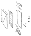
- a transmission-type display device P is illuminated by a backlight device according to the invention including light sources 1, reflectors 2, a reflection means 10 and a transmission member 11 having a pattern of reflection layer.
- the light sources are disposed outside the display device P to form an edge-type or H(-arrangement)-type backlight device.
- the lamps are disposed with a spacing of at least M which is a lateral length of the display device P.
- the light source 1 may be any light source having a spectral distribution desired by the display device P. Specific examples thereof may include LEDs, halogen lamps, xenon lamps and white fluorescent lamps. Particularly, for a display device having three types of pixels of red (R), green (G) and blue (B), it is preferred to use a three-wavelength type white fluorescent lamp having a spectral characteristic of providing emission peaks in the regions of R, G and B, respectively.
- the reflectors 2 and reflecting means 10 may for example comprise a metal member having a reflecting inner surface or a light-absorbing or light-transmissive substrate coated with a reflective material forming an inner surface.
- the transmission member 11 may comprise a light-transmissive substrate surface-coated with pattern of reflection layer.
- the reflection layer pattern may preferably have apertures (portions free from the reflection layer) occupying an areal ratio (i.e., aperture ratio) which increases with an increase in distance in X-direction from a light source 1.
- aperture ratio is determined based on distances of 0 to M/2 from the light sources at the left and right ends.
- the reflection layer may have a pattern of a multitude of reflective portions of various shape, such as circles, ellipses, squares, rectangles, lozenges, parallelograms, trapezoids or stars.
- the apertures can assume various discrete shapes as descried above.
- the display device P may suitably comprise a liquid crystal device, examples of which may include: STN-type and DSTN-type liquid crystal devices using nematic liquid crystals; active matrix-type liquid crystal devices using thin-film transistors or MIM-elements; and ferroelectric liquid crystal devices and anti-ferroelectric liquid crystal devices using chiral smectic liquid crystals.
- a liquid crystal device examples of which may include: STN-type and DSTN-type liquid crystal devices using nematic liquid crystals; active matrix-type liquid crystal devices using thin-film transistors or MIM-elements; and ferroelectric liquid crystal devices and anti-ferroelectric liquid crystal devices using chiral smectic liquid crystals.
- the backlight device according to the present comparative example may preferably further comprise a prism sheet so as to have the direction of light issuance therefrom approach a planar normal.
- a prism sheet so as to have the direction of light issuance therefrom approach a planar normal.
- the reflecting means with a reflecting surface shaped so as to reduce the number of reflections thereat as will be described with reference to Figures 17 and 18, while a shaping step may be additionally required thereby.
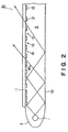
- a backlight device B 1 shown in Figure 2 is provided with a rear reflecting plate (reflection means) 10 composed of an aluminium plate.
- the rear reflecting plate 10 has a mirror-finished surface so as to reflect light incident thereto.
- the reflecting plate is integrally formed with reflectors 2 having a concave surface composed also of an aluminum plate.
- a front transmission plate (transmission member) 11 of a thin transparent acrylic resin plate is disposed with a spacing from and in parallel with the reflecting plate 10, so that a space S is defined by the rear reflecting plate 10 and the front transmission plate 11.
- three wavelength-type fluorescent lamps 1 as linear light sources are disposed so that light emitted therefrom enters the space S directly or indirectly after reflection by the reflector 2.
- a reflection layer 12 of, e.g., vapour-deposited aluminium is disposed in a pattern of a mesh or various discrete shapes as described above to form a multitude of apertures 13, out of which light is allowed to leak out through the front transmission plate 11.
- a transmission-type liquid crystal panel (not shown) so that the liquid crystal panel is illuminated with the light issued from the backlight device B 1 .
- the angle (denoted by “ ⁇ 1 " in Figure 2) of light incident to the transmission plate 11 becomes smaller as the position leaves away from the fluorescent lamp 1 so that leakage quantity of the light becomes smaller in proportion to almost the angle ⁇ 1 , if the aperture ratio k is constant.
- the aperture ratio k(x) of the reflection layer 12 is set to be larger as the distance x increases, so that the leakage light quantities at various positions become substantially equal.
- the planar luminance distribution of the leakage light (illumination light) from the backlight device B 1 becomes uniform to provide an improved display quality to the liquid crystal panel.
- the light-guide member 3 ( Figure 21) required in the conventional device is omitted, so that the backlight device becomes lighter in weight by that much and provides an improved portability to even a large-area display apparatus.
- a front surface (opposite to a transmission plate 11 and a reflection layer 12) of a rear reflection plate 10 is provided with a scattering layer 20.
- the scattering layer 20 may be composed of a printed layer of a white pigment, such as barium sulphate, calcium carbonate or titanium oxide and, likewise the reflection layer 12, may be formed in a mesh pattern or a discrete dot pattern so as to provide a multitude of apertures 21.
- the aperture ratio k 1 (x) of the scattering layer 20 is set to be smaller as the distance from the fluorescent lamp increases, in contrast to the case of the reflection layer 12.
- the aperture ratio k(x) of the reflection layer 12 is set to be larger as the distance x from the fluorescent lamp 1 becomes larger, so that the leakage light quantities at various positions become almost equal.
- the leakage light (illumination light) from the backlight device B 2 is caused to have a uniform planar luminance distribution, thereby providing an improved display quality to the liquid crystal panel.
- the incident light angle ⁇ 2 becomes smaller as the position is left away from the fluorescent lamp 1.
- the aperture ratio k 1 (x) of the scattering layer is set to be smaller so as to provide a larger occupation areal ratio (1-k 1 (x)) of the scattering layer 20 as the position is left away from the fluorescent lamp 1.
- the scattered light is incident to the transmission plate 11 at a larger incident angle ⁇ 3 to be more readily leaked out through the apertures 13 of the reflection layer 2.
- the backlight device can exhibit an improved performance for a larger area display apparatus.
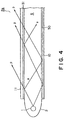
- a front surface (upper surface) of a rear reflection plate 10 is provided with a ⁇ /4 plate 30 for effecting plarization conversion between an s-polarization component (light component having an electric field component perpendicular to the drawing sheet of Figure 4) and a p-polarization component (light component having an electric field component parallel to the drawing sheet of Figure 4), and a lower surface of a front transmission plate 11 is provided with a polarization beam splitter layer 31 of an optical multi-layer film, which allows the transmission of only the p-polarization component and reflects the s-polarization component.
- a liquid crystal panel (not shown) disposed above the plat 11 is designed to receive the p-polarized light as illumination light.
- the fluorescent lamp 1 When the fluorescent lamp 1 is turned on, emitted light is repetitively reflected between the rear reflecting plate 10 and the polarization beam splitter layer 31, and a p-polarization component of the light incident to the polarization beam splitter layer 31 is transmitted through the layer 31 and the front transmission plate 11 to be leaked outwards.
- the remaining s-polarization component is reflected by the polarization beam splitter layer 31 and then incident to and reflected by the rear reflection plate 10 where the s-polarization is converted to p-polarization because it passes twice the ⁇ /4 plate 30.
- the resultant p-polarization component is transmitted through the polarization beam splitter layer 31 and the front transmission plat 11 to be leaked outwards.
- the illumination efficiency of the backlight device can be remarkably improved.
- a front transmission plate 11 is composed of a transparent glass plate and the front surface of the front transmission plate 11 is provided with a reflection layer 12. Further, between a rear reflection plate 10 and a ⁇ /4 plate 30, a scattering layer 20 is disposed.
- the reflection layer 12 is formed in a dot pattern or a mesh pattern so as to have an aperture ratio k(x) increasing with an increase in distance from the fluorescent lamp 1 similarly as in the first embodiment, and the scattering layer 20 is formed in a dot or mesh pattern so as to provide a prescribed aperture ratio k 1 (x) similarly as in the second embodiment.
- an s-polarization component is reflected by a polarization beam splitter layer 31 and is then reflected by a rear reflection plate 10 where it is converted into a p-polarization component.
- a p-polarization component is transmitted through the polarization beam splitter 31, a portion thereof is leaked out of the apertures 13 to illuminate a liquid crystal panel (not shown) disposed above, and the remaining portion thereof is reflected by the reflection layer 12 to enter the space S again.
- the portion of the p-polalization component reffected by the reflection layer 12 is converted into an s-polarization component when it is reflected by the rear reflection plate 10.
- the s-polarization component is again reflected by the polarization beam splitter layer 31 and the rear reflection plate 10, where it is again converted into a p-polarization component allowed to be leaked outwards similarly as the above for illuminating the liquid crystal panel.
- the aperture ratio k(x) of the reflection layer 12 is set to be larger as thesdistance x from the fluorescent lamp 1 increases, the light leakage quantities at various positions become almost equal, so that the leakage light (illumination light) from the backlight device is caused to have a uniform planar luminance distribution, thereby providing an improved display quality to the liquid crystal panel.
- the illumination light angle characteristic is uniformized regardless of the distance from the fluorescent lamp 1 and the leakage light quantities at various positions are made almost equal, so that the planar luminance distribution is uniformized also in this respect to provide an improved display quality of the liquid crystal panel.
- the aperture ratio k 1 (x) of the scattering layer 20 is set to be smaller as the distance x from the fluorescent lamp 1 increases, a fraction of light incident at a smaller incident angle ⁇ 2 is more easily scattered, so that the leakage light quantities from various positions of the backlight device are equalized also in this respect, leading to a uniform planar luminance distribution of the backlight device B 4 and an improved display quality of the liquid crystal panel.
- the utilization efficiency of the backlight illumination light can be remarkably improved.
- the fluorescent lamp 1 is indicated but it is possible to dispose an additional fluorescent lamp at a position opposite to the fluorescent lamp 1 so as to dispose the reflection plate 10 and the transmission plate 11 between the resultant pair of fluorescent lamps similarly as shown in Figure 1.
- the number of fluorescent lamps is not limited to 2 but may be 4 so as to surround the space S. By this arrangement, it is possible to provide a backlight device with an increased luminous intensity.
- the reflection layer 12 is disposed on the upper surface of the front transmission plate but this is not limitative.
- a reflection layer may also be disposed on a lower surface (confronting with the ⁇ /4 plate 30) of the front transmission plate 11.
- the apertures in the reflection layer are arranged to have an aperture ratio which increases with an increase in distance from a light source, the light leakage quantities at respective positions are substantially equalized to provide a uniform planar luminance distribution of leakage light (illumination light).
- the reflection means is provided with a scattering layer for scattering and reflecting light incident thereto, the angle characteristic of issued light can be uniformized to equalize the leakage light quantities, thereby providing a uniform planar luminance distribution of illumination light.
- the scattering layer is provided with a multitude of apertures providing an aperture ratio which decreases with an increase in distance from the light source, a light fraction having a smaller incident angle is subjected to a promoted scattering to increase the light leakage through the apertures of the reflection layer thereat. This also promotes the equalization of leakage lights from the backlight device leading to a uniform planar luminance distribution of illumination light.
- Figures 11 and 12 are respectively a plan view showing a preferred reflection layer pattern (aperture pattern) used in the present invention.
- the X-Y coordinates in these figures correspond to that shown in Figure 1, and a larger x represents a larger distance from a light source 1.
- the reflection layer pattern is depicted only one-dimensionally in the X-direction but actually the pattern may be repeated in the Y direction.
- the reflective layer patterns shown in Figures 11 and 12 respectively include a sub-pattern 12a and a sub-pattern 12b.
- the sub-pattern 12a comprises a continuous masking layer (shown with a hatching, illustrated as discrete square patterns for convenience of illustration but may actually constitute a continuous layer) and discrete apertures having an aperture ratio increasing with an increase in X-coordinate.
- the sub-pattern 12a is suitable for providing aperture ratios in a range of, e.g., 0 - 50 %.
- the sub-pattern 12b is a negative (or complementary) pattern with respect to the sub-pattern 12a, i.e., comprises discrete masking layers and a continuous aperture (or opening) area surrounding the masking layers.
- the sub-pattern 12b is suitable for providing aperture ratios in the range of, e.g., 50 - 100 %. It is clear that the boundary aperture ratio for selection of the sub-patterns 12a and 12b is not necessarily 50 %.
- the patterns of Figures 11 and 12 may be formed laterally symmetrically with a line (extending longitudinally) of aperture ratio of 100 % at the center.
- the data transmission apparatus 400 includes a liquid crystal panel (display device) P so as to display various data or information by the panel P.
- a liquid crystal panel includes a pair of oppositely disposed substrates, and a liquid crystal disposed between the substrates.
- the pair of substrates are provided with scanning electrodes and data electrodes so as to form an electrode matrix.
- the liquid crystal panel P is connected to a scanning signal application circuit 402 and a data signal transmission circuit 403, which are in turn further connected to a scanning signal control circuit 404 and a data signal control circuit 406, a drive control circuit 405 and a graphic controller 407, sequentially.
- data and scanning scheme signals are supplied from the graphic controller 407 via the drive control circuit 405 to the scanning signal control circuit 404 and the data signal control circuit 406, where the data are converted into address data and display data and the other scanning scheme signals are sent as they are to the scanning signal application circuit 402 and the data signal application circuit 403.
- the scanning signal application circuit 402 applies a scanning signal having a waveform determined by the scanning scheme signals to a scanning electrode determined by the address data
- the data signal application circuit 403 applies data signals having waveforms determined by both display contents of white or black based on the display data and the scanning scheme signals.
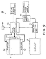
- a liquid crystal display apparatus 50 is provided with a backlight device according to any one of the above-descried embodiments.
- the backlight device 10 is connected to a backlight lighting circuit (backlight drive means) 51 so as to drive the backlight device 10.
- a liquid crystal panel P which comprises a pair of oppositely disposed glass substrates provided with scanning electrodes and data electrodes, and a ferroelectric liquid crystal disposed between the glass substrates.
- the scanning electrodes and data electrodes are connected to X-drivers 52 and a Y-driver 53, respectively, which in turn are corrected to a panel drive controller (liquid crystal device drive means) 55.
- the panel drive controller 55 and the backlight lighting circuit 51 are connected to a power supply unit 56 so as to supply powers. Further, panel drive controller is connected to a host computer (not shown) to be supplied with display signals. On the other hand, based on the display signals, the panel drive controller 55 supplies signals to the liquid crystal panel P via the drivers 52 and 53. Further, the panel drive controller 55 supplies ON/OFF signals and lighting control signals to the backlight lighting circuit 51, which drives the backlight device 10 based on such signals.
Landscapes
- Physics & Mathematics (AREA)
- General Physics & Mathematics (AREA)
- Optics & Photonics (AREA)
- Nonlinear Science (AREA)
- General Engineering & Computer Science (AREA)
- Engineering & Computer Science (AREA)
- Crystallography & Structural Chemistry (AREA)
- Chemical & Material Sciences (AREA)
- Mathematical Physics (AREA)
- Astronomy & Astrophysics (AREA)
- Liquid Crystal (AREA)
- Planar Illumination Modules (AREA)
- Devices For Indicating Variable Information By Combining Individual Elements (AREA)
- Light Guides In General And Applications Therefor (AREA)
- Non-Portable Lighting Devices Or Systems Thereof (AREA)
Claims (2)
- Dispositif d'éclairage par l'arrière globalement rectangulaire et plan ayant des faces planes principales avant et arrière, comportant:une source de lumière (1) disposée le long d'un côté du dispositif d'éclairage par l'arrière;un diviseur (31) de faisceau à polarisation disposé le long de la face plane principale avant du dispositif d'éclairage par l'arrière pour transmettre sélectivement l'une d'une composante de polarisation p, ayant une composante de champ électrique perpendiculaire au diviseur (31) de faisceau à polarisation, et d'une composante de polarisation s, ayant une composante de champ électrique parallèle au diviseur (31) de faisceau à polarisation, de la lumière émise depuis la source de lumière (1), lors de l'utilisation, et pour réfléchir l'autre de la composante de polarisation p et de la composante de polarisation s;un moyen (10, 30) de réflexion et de conversion de polarisation disposé le long de la face plane principale arrière du dispositif d'éclairage par l'arrière pour réfléchir de la lumière et effectuer une conversion de polarisation entre la composante de polarisation s et la composante de polarisation p;grâce à quoi de la lumière émise depuis la source de lumière (1) dans une région s entre le diviseur (31) de faisceau à polarisation et le moyen (10, 30) de réflexion et de conversion de polarisation est réfléchie entre le diviseur (31) de faisceau à polarisation et le moyen (10, 30) de réflexion et de conversion de polarisation afin que la composante de polarisation p ou la composante de polarisation s de la lumière émise sorte en fuyant sélectivement à travers le diviseur (31) de faisceau à polarisation.
- Dispositif d'éclairage par l'arrière selon la revendication 1, dans lequel le moyen de réflexion et de conversion de polarisation comprend un moyen de réflexion (10) disposé le long de la face plane principale arrière du dispositif d'éclairage par l'arrière, agencé pour envoyer par réflexion de la lumière dans le dispositif d'éclairage par l'arrière, et une lame quart d'onde (30) destinée à effectuer une conversion de polarisation, disposée de façon à être adjacente au moyen de réflexion (10) sur le côté du moyen de réflexion (10) faisant face au diviseur (31) de faisceau à polarisation.
Priority Applications (1)
| Application Number | Priority Date | Filing Date | Title |
|---|---|---|---|
| EP01202333A EP1139013B1 (fr) | 1994-05-27 | 1995-05-26 | Dispositif d'éclairage par l'arrière pour afficheur |
Applications Claiming Priority (6)
| Application Number | Priority Date | Filing Date | Title |
|---|---|---|---|
| JP137894/94 | 1994-05-27 | ||
| JP13789494 | 1994-05-27 | ||
| JP13789494 | 1994-05-27 | ||
| JP42194/95 | 1995-03-01 | ||
| JP4219495 | 1995-03-01 | ||
| JP4219495 | 1995-03-01 |
Related Child Applications (1)
| Application Number | Title | Priority Date | Filing Date |
|---|---|---|---|
| EP01202333A Division EP1139013B1 (fr) | 1994-05-27 | 1995-05-26 | Dispositif d'éclairage par l'arrière pour afficheur |
Publications (3)
| Publication Number | Publication Date |
|---|---|
| EP0684423A2 EP0684423A2 (fr) | 1995-11-29 |
| EP0684423A3 EP0684423A3 (fr) | 1996-04-24 |
| EP0684423B1 true EP0684423B1 (fr) | 2002-10-02 |
Family
ID=26381843
Family Applications (2)
| Application Number | Title | Priority Date | Filing Date |
|---|---|---|---|
| EP95303585A Expired - Lifetime EP0684423B1 (fr) | 1994-05-27 | 1995-05-26 | Dispositif d'éclairage par l'arrière pour afficheur |
| EP01202333A Expired - Lifetime EP1139013B1 (fr) | 1994-05-27 | 1995-05-26 | Dispositif d'éclairage par l'arrière pour afficheur |
Family Applications After (1)
| Application Number | Title | Priority Date | Filing Date |
|---|---|---|---|
| EP01202333A Expired - Lifetime EP1139013B1 (fr) | 1994-05-27 | 1995-05-26 | Dispositif d'éclairage par l'arrière pour afficheur |
Country Status (9)
| Country | Link |
|---|---|
| US (1) | US5816677A (fr) |
| EP (2) | EP0684423B1 (fr) |
| JP (1) | JP2000284707A (fr) |
| KR (1) | KR100215998B1 (fr) |
| CN (1) | CN1052310C (fr) |
| AT (2) | ATE225487T1 (fr) |
| AU (1) | AU670403B2 (fr) |
| CA (1) | CA2150340C (fr) |
| DE (2) | DE69534884T2 (fr) |
Cited By (2)
| Publication number | Priority date | Publication date | Assignee | Title |
|---|---|---|---|---|
| US6590705B1 (en) | 1996-02-29 | 2003-07-08 | 3M Innovative Properties Company | Optical film with co-continuous phases |
| US8482698B2 (en) | 2008-06-25 | 2013-07-09 | Dolby Laboratories Licensing Corporation | High dynamic range display using LED backlighting, stacked optical films, and LCD drive signals based on a low resolution light field simulation |
Families Citing this family (114)
| Publication number | Priority date | Publication date | Assignee | Title |
|---|---|---|---|---|
| DE69721505T2 (de) * | 1996-02-29 | 2003-11-20 | Minnesota Mining And Manufacturing Company, St. Paul | Film zur helligkeitserhoehung |
| US5867316A (en) * | 1996-02-29 | 1999-02-02 | Minnesota Mining And Manufacturing Company | Multilayer film having a continuous and disperse phase |
| US5783120A (en) * | 1996-02-29 | 1998-07-21 | Minnesota Mining And Manufacturing Company | Method for making an optical film |
| US5825543A (en) * | 1996-02-29 | 1998-10-20 | Minnesota Mining And Manufacturing Company | Diffusely reflecting polarizing element including a first birefringent phase and a second phase |
| JPH09269418A (ja) * | 1996-03-29 | 1997-10-14 | Enplas Corp | 光制御部材及び面光源装置 |
| JP3409587B2 (ja) | 1996-05-14 | 2003-05-26 | オムロン株式会社 | 光路変換光学素子、画像表示装置及び光投射器 |
| TW383508B (en) * | 1996-07-29 | 2000-03-01 | Nichia Kagaku Kogyo Kk | Light emitting device and display |
| JP3271695B2 (ja) * | 1996-09-20 | 2002-04-02 | シャープ株式会社 | バックライト光源および液晶表示装置 |
| JP3538746B2 (ja) * | 1997-03-07 | 2004-06-14 | 株式会社エンプラス | サイドライト型面光源装置 |
| JPH10260404A (ja) * | 1997-03-18 | 1998-09-29 | Seiko Epson Corp | 照明装置、液晶表示装置及び電子機器 |
| US6024462A (en) * | 1997-06-10 | 2000-02-15 | The University Of British Columbia | High efficiency high intensity backlighting of graphic displays |
| US6104455A (en) * | 1997-08-27 | 2000-08-15 | Dai Nippon Printing Co., Ltd. | Back light device and liquid crystal display apparatus |
| JPH11125834A (ja) | 1997-10-24 | 1999-05-11 | Canon Inc | マトリクス基板及び液晶表示装置と投写型液晶表示装置 |
| US6274516B1 (en) | 1997-10-27 | 2001-08-14 | Canon Kabushiki Kaisha | Process for manufacturing interlayer insulating film and display apparatus using this film and its manufacturing method |
| JP3199312B2 (ja) | 1997-11-06 | 2001-08-20 | キヤノン株式会社 | 液晶表示装置 |
| JP3308880B2 (ja) | 1997-11-07 | 2002-07-29 | キヤノン株式会社 | 液晶表示装置と投写型液晶表示装置 |
| JP2000030515A (ja) * | 1998-07-09 | 2000-01-28 | Sony Corp | 面状照明装置 |
| US6005713A (en) * | 1998-08-21 | 1999-12-21 | 3M Innovative Properties Company | Multilayer polarizer having a continuous and disperse phase |
| DE19851635A1 (de) * | 1998-11-10 | 2000-06-29 | Bosch Gmbh Robert | Beleuchtungsanordnung und Anzeigeaggregat |
| DE19858810A1 (de) * | 1998-12-21 | 2000-06-29 | Patent Treuhand Ges Fuer Elektrische Gluehlampen Mbh | Flache Beleuchtungsvorrichtung und Betriebsverfahren |
| WO2000063738A1 (fr) * | 1999-04-21 | 2000-10-26 | U.S. Precision Lens Incorporated | Systemes optiques pour afficheurs a cristaux liquides reflechissants |
| JP2003500813A (ja) | 1999-05-20 | 2003-01-07 | ツムトーベル シュタッフ ゲゼルシャフト ミット ベシュレンクテル ハフツング | 照明装置 |
| DE19961491B4 (de) * | 1999-05-25 | 2005-08-04 | Siteco Beleuchtungstechnik Gmbh | Innenraumleuchte mit Hohllichtleiter |
| DE10011378B4 (de) * | 1999-05-25 | 2013-07-25 | Siteco Beleuchtungstechnik Gmbh | Hohllichtleiterleuchte mit indirekter Lichtabstrahlung |
| US6502946B1 (en) * | 1999-07-21 | 2003-01-07 | Nippon Sheet Glass Co., Ltd. | Planar display lamp and method of forming a light scatterer pattern |
| KR100356991B1 (ko) * | 1999-08-19 | 2002-10-18 | 엘지.필립스 엘시디 주식회사 | 백라이트 유닛 |
| JP4198281B2 (ja) * | 1999-09-13 | 2008-12-17 | 日本ライツ株式会社 | 導光板および平面照明装置 |
| TW454098B (en) * | 1999-12-31 | 2001-09-11 | Lee Chih Kung | The configuration of a backlight module that can control the polarization state of the output light beams |
| US6893135B2 (en) * | 2000-03-16 | 2005-05-17 | 3M Innovative Properties Company | Light guides suitable for illuminated displays |
| US7525531B2 (en) * | 2000-07-31 | 2009-04-28 | Toshiba Matsushita Display Technology Co., Ltd. | Method for manufacturing lighting device, image display, liquid crystal monitor, liquid crystal television, liquid crystal information terminal, and light guide plate |
| WO2002011406A2 (fr) | 2000-07-31 | 2002-02-07 | Koninklijke Philips Electronics N.V. | Dispositif d'affichage detecteur d'image |
| AU2001284844A1 (en) | 2000-08-18 | 2002-03-04 | Reflexite Corporation | Differentially cured materials and process for forming same |
| US20040190102A1 (en) * | 2000-08-18 | 2004-09-30 | Mullen Patrick W. | Differentially-cured materials and process for forming same |
| US7230764B2 (en) * | 2000-08-18 | 2007-06-12 | Reflexite Corporation | Differentially-cured materials and process for forming same |
| JP2002148615A (ja) * | 2000-11-08 | 2002-05-22 | Nitto Denko Corp | 光学フィルム及び反射型液晶表示装置 |
| JP2002207433A (ja) * | 2001-01-10 | 2002-07-26 | Dainippon Printing Co Ltd | 自己発光型ディスプレイ |
| EP1315022A1 (fr) * | 2001-11-27 | 2003-05-28 | Thomson Licensing, Inc. | Polariseur a recyclage de polarisation |
| US6880946B2 (en) * | 2002-01-15 | 2005-04-19 | Reflexite Corporation | Grooved optical microstructure light collimating films |
| TW200302940A (en) | 2002-02-01 | 2003-08-16 | Samsung Electronics Co Ltd | Liquid crystal display device |
| KR100874744B1 (ko) * | 2002-02-04 | 2008-12-19 | (주)바이오니아 | 레지오넬라 균종의 리보핵산 중합효소 베타 서브유닛의데옥시리보핵산 분절과 이에 선택적인 프라이머, 이를이용한 레지오넬라 균종의 판별 방법 |
| KR100880217B1 (ko) * | 2002-07-24 | 2009-01-28 | 엘지디스플레이 주식회사 | 백라이트 |
| JP3923867B2 (ja) * | 2002-07-26 | 2007-06-06 | 株式会社アドバンスト・ディスプレイ | 面状光源装置及びそれを用いた液晶表示装置 |
| TWI289708B (en) | 2002-12-25 | 2007-11-11 | Qualcomm Mems Technologies Inc | Optical interference type color display |
| JP4029743B2 (ja) * | 2003-02-24 | 2008-01-09 | ソニー株式会社 | バックライト |
| JP2004261996A (ja) * | 2003-02-28 | 2004-09-24 | Rohm Co Ltd | プリントヘッドおよび画像形成装置 |
| CN1833183A (zh) * | 2003-05-02 | 2006-09-13 | 瑞弗莱克塞特公司 | 改变光线方向的光学结构 |
| US6974229B2 (en) * | 2003-05-21 | 2005-12-13 | Lumileds Lighting U.S., Llc | Devices for creating brightness profiles |
| KR100995640B1 (ko) | 2003-07-07 | 2010-11-19 | 엘지디스플레이 주식회사 | 액정표시모듈 |
| TWI308242B (en) * | 2003-10-24 | 2009-04-01 | Hon Hai Prec Ind Co Ltd | Light guiding device and backlight module using the same |
| US7342705B2 (en) | 2004-02-03 | 2008-03-11 | Idc, Llc | Spatial light modulator with integrated optical compensation structure |
| CA2573689C (fr) | 2004-07-27 | 2012-09-18 | The University Of British Columbia | Diffuseur de lumiere provenant d'un reseau de sources lumineuses et dispositifs d'affichage comprenant ce diffuseur |
| JP4604801B2 (ja) * | 2004-12-27 | 2011-01-05 | 三菱電機株式会社 | 面状光源装置および該装置を用いた表示装置 |
| CN100416370C (zh) * | 2004-12-27 | 2008-09-03 | 三菱电机株式会社 | 面状光源装置及使用了该装置的显示装置 |
| EP1696260B1 (fr) | 2005-02-08 | 2013-09-25 | BMG Gesellschaft für moderne Informationssysteme mbH | Dispositif d'affichage à cristaux liquides et agencement d'affichage à cristaux liquides comprenant une pluralité de tels dispositifs d'affichage à cristaux liquides |
| US20060182409A1 (en) * | 2005-02-11 | 2006-08-17 | Eastman Kodak Company | Optical films of differing refractive indices |
| JP2006234849A (ja) * | 2005-02-21 | 2006-09-07 | Nec Lcd Technologies Ltd | 液晶表示装置及び該液晶表示装置に用いられる駆動方法 |
| KR100705737B1 (ko) * | 2005-04-08 | 2007-04-09 | 강봉섭 | 다중 반사면의 반사판을 구비한 백라이트 유닛 |
| KR101212136B1 (ko) * | 2005-06-29 | 2012-12-14 | 엘지디스플레이 주식회사 | 프리즘 시트와 이를 이용한 백 라이트 유닛 |
| JP4895158B2 (ja) * | 2005-08-26 | 2012-03-14 | 国立大学法人東北大学 | 液晶ディスプレイ |
| JP4579146B2 (ja) | 2005-12-06 | 2010-11-10 | 株式会社 日立ディスプレイズ | 表示装置および面状光源装置 |
| KR100781350B1 (ko) | 2005-12-26 | 2007-11-30 | 주식회사 바다테크 | 고휘도 백라이트장치 |
| DE102006007065A1 (de) * | 2006-02-15 | 2007-08-16 | BSH Bosch und Siemens Hausgeräte GmbH | Vorrichtung zur Hintergrundbeleuchtung einer LC-Anzeigeeinrichtung für eine Anzeige- und/oder Bedienungseinheit, insbesondere in einem Hausgerät |
| US7876489B2 (en) * | 2006-06-05 | 2011-01-25 | Pixtronix, Inc. | Display apparatus with optical cavities |
| EP1943551A2 (fr) | 2006-10-06 | 2008-07-16 | Qualcomm Mems Technologies, Inc. | Guide de lumière |
| ATE556272T1 (de) | 2006-10-06 | 2012-05-15 | Qualcomm Mems Technologies Inc | Optische verluststruktur in einer beleuchtungsvorrichtung |
| KR101340800B1 (ko) | 2006-11-02 | 2013-12-11 | 엘지디스플레이 주식회사 | 반사시트 및 이를 구비하는 표시장치 |
| TWI359988B (en) * | 2007-04-13 | 2012-03-11 | Chimei Innolux Corp | Liquid crystal display and backlight module thereo |
| CN101303478B (zh) * | 2007-05-09 | 2011-09-14 | 奇美电子股份有限公司 | 液晶显示装置及其背光模块 |
| TWI439641B (zh) | 2007-05-20 | 2014-06-01 | 3M Innovative Properties Co | 用於側面發光型背光之準直光注入器 |
| TWI448643B (zh) | 2007-05-20 | 2014-08-11 | 3M Innovative Properties Co | 背光與利用背光之顯示系統 |
| CN101681053B (zh) | 2007-05-20 | 2012-03-21 | 3M创新有限公司 | 具有半镜面元件的循环背光源 |
| CN101681057B (zh) | 2007-05-20 | 2012-07-04 | 3M创新有限公司 | 光循环型薄壁中空腔体背光源 |
| CN101779148B (zh) | 2007-06-14 | 2014-06-25 | 艾利丹尼森公司 | 受照图形和信息显示器 |
| US8092062B2 (en) * | 2007-08-29 | 2012-01-10 | Sharp Kabushiki Kaisha | Light-emitting element and display unit having the same |
| US8068710B2 (en) | 2007-12-07 | 2011-11-29 | Qualcomm Mems Technologies, Inc. | Decoupled holographic film and diffuser |
| EP2255231A1 (fr) * | 2008-02-07 | 2010-12-01 | 3M Innovative Properties Company | Rétroéclairage creux comportant des films structurés |
| WO2009100303A1 (fr) * | 2008-02-08 | 2009-08-13 | 3M Innovative Properties Company | Rétroéclairage perforé |
| WO2009102733A2 (fr) * | 2008-02-12 | 2009-08-20 | Qualcomm Mems Technologies, Inc. | Diffuseur de lumiere avant integre pour afficheurs reflechissants |
| WO2009105450A1 (fr) | 2008-02-22 | 2009-08-27 | 3M Innovative Properties Company | Rétroéclairages ayant des répartitions de flux lumineux de sortie sélectionnées et systèmes d’affichage qui utilisent ces rétroéclairages |
| EP2297607B1 (fr) * | 2008-06-04 | 2014-04-23 | 3M Innovative Properties Company | Panneau lumineux creux avec source de lumière basculée |
| JP5571889B2 (ja) * | 2008-08-29 | 2014-08-13 | 株式会社東芝 | 発光装置及び照明装置 |
| KR20100038684A (ko) * | 2008-10-06 | 2010-04-15 | 삼성전자주식회사 | 백라이트 유닛 및 이를 이용한 영상표시장치 |
| US20100110724A1 (en) * | 2008-10-24 | 2010-05-06 | Scott Moncrieff | Thin film light diffusion guide |
| USD620189S1 (en) | 2009-05-22 | 2010-07-20 | Coleman Hill | Protective casing for exterior lighting fixtures |
| US9341887B2 (en) | 2009-09-11 | 2016-05-17 | Dolby Laboratories Licensing Corporation | Displays with a backlight incorporating reflecting layer |
| US20110219648A1 (en) * | 2010-03-12 | 2011-09-15 | Trevor James | Led edge-lit signage utilizing digital print technology |
| JP5045826B2 (ja) * | 2010-03-31 | 2012-10-10 | ソニー株式会社 | 光源デバイスおよび立体表示装置 |
| CN201773867U (zh) * | 2010-07-12 | 2011-03-23 | 国基电子(上海)有限公司 | 多层交错布点导光元件结构 |
| USD654213S1 (en) * | 2010-09-21 | 2012-02-14 | Sergey Nersesov | Lighting appliance |
| TWI465808B (zh) | 2010-11-25 | 2014-12-21 | Lg伊諾特股份有限公司 | 背光單元及其顯示設備 |
| US8902484B2 (en) | 2010-12-15 | 2014-12-02 | Qualcomm Mems Technologies, Inc. | Holographic brightness enhancement film |
| KR20120131360A (ko) * | 2011-05-25 | 2012-12-05 | 삼성전자주식회사 | 면조명장치 및 이를 구비한 액정표시장치 |
| US9541964B2 (en) * | 2012-01-10 | 2017-01-10 | Lg Electronics Inc. | Image module, mobile terminal having the same and manufacturing method of image module |
| CN102635817B (zh) * | 2012-03-29 | 2014-02-26 | 深圳市华星光电技术有限公司 | 背光模组及液晶显示器 |
| CN202629814U (zh) * | 2012-05-31 | 2012-12-26 | 京东方科技集团股份有限公司 | 侧入式背光模组 |
| US9632357B2 (en) | 2012-07-17 | 2017-04-25 | Lg Electronics Inc. | Display device |
| KR20140020493A (ko) * | 2012-08-08 | 2014-02-19 | 삼성디스플레이 주식회사 | 도광판 및 그 제조 방법 |
| KR101992362B1 (ko) * | 2012-08-29 | 2019-06-24 | 엘지이노텍 주식회사 | 라이트 유닛 및 그를 이용한 조명 시스템 |
| BR112015009327A2 (pt) | 2012-10-30 | 2017-08-22 | 3M Innovative Properties Company | Elemento de iluminação, sistema de iluminação e método para iluminar uma região |
| US9791128B2 (en) | 2012-10-30 | 2017-10-17 | 3M Innovative Properties Company | Curved light duct extraction |
| US9400349B2 (en) * | 2012-11-09 | 2016-07-26 | Apple Inc. | Electronic device with display chassis structures |
| CN103148453A (zh) * | 2013-03-12 | 2013-06-12 | 京东方科技集团股份有限公司 | 导光板、光学膜片、背光模组、阵列基板及液晶模组 |
| US9803833B2 (en) * | 2013-12-03 | 2017-10-31 | X Development Llc | Multi-aperture illumination layer for tileable display |
| JP6359898B2 (ja) * | 2014-07-03 | 2018-07-18 | シャープ株式会社 | 照明装置、画像読取装置及びそれを備えた画像形成装置 |
| CN104676379B (zh) * | 2015-02-26 | 2017-06-30 | 深圳市华星光电技术有限公司 | 背光模组及包含其的液晶显示装置 |
| CN104613385A (zh) * | 2015-02-26 | 2015-05-13 | 深圳市华星光电技术有限公司 | 液晶显示器及背光模组 |
| JP6762813B2 (ja) * | 2015-09-28 | 2020-09-30 | 日東電工株式会社 | 液晶表示装置 |
| KR20170126563A (ko) * | 2016-05-09 | 2017-11-20 | 삼성디스플레이 주식회사 | 광학 부재 및 이를 포함하는 표시 장치 |
| CN106154397A (zh) * | 2016-07-05 | 2016-11-23 | 武汉华星光电技术有限公司 | 用于透反式显示面板的背光模组和透反式液晶显示模组 |
| CN106896566B (zh) * | 2017-03-14 | 2021-08-13 | 京东方科技集团股份有限公司 | 一种背光结构和液晶显示设备 |
| CN108153060A (zh) * | 2018-02-01 | 2018-06-12 | 广东欧珀移动通信有限公司 | 背光模组、显示装置和电子设备 |
| KR20200113061A (ko) * | 2019-03-20 | 2020-10-06 | 희성전자 주식회사 | 디스플레이용 백라이트 장치 |
| KR20200113062A (ko) * | 2019-03-20 | 2020-10-06 | 희성전자 주식회사 | 디스플레이용 백라이트 장치 |
| JP2023096907A (ja) * | 2021-12-27 | 2023-07-07 | シャープディスプレイテクノロジー株式会社 | 液晶表示素子 |
Family Cites Families (29)
| Publication number | Priority date | Publication date | Assignee | Title |
|---|---|---|---|---|
| JPS57128383A (en) * | 1981-02-02 | 1982-08-09 | Mitsubishi Electric Corp | Surface lighting apparatus |
| JPS57174803A (en) * | 1981-04-20 | 1982-10-27 | Masayasu Negishi | Surface light source device |
| US4510559A (en) * | 1983-08-08 | 1985-04-09 | Mcgraw-Edison Company | Lamp and filter mounting assembly |
| JPH07120143B2 (ja) * | 1986-06-04 | 1995-12-20 | キヤノン株式会社 | 表示パネルの情報読出し法及び表示パネルの情報読出し装置 |
| JPS6313202A (ja) * | 1986-07-03 | 1988-01-20 | キヤノン株式会社 | 光源装置 |
| JPS63168626A (ja) * | 1987-01-06 | 1988-07-12 | Citizen Watch Co Ltd | 液晶表示体 |
| US4874228A (en) * | 1987-03-24 | 1989-10-17 | Minnesota Mining And Manufacturing Company | Back-lit display |
| JPH0731323B2 (ja) * | 1988-04-01 | 1995-04-10 | 三菱レイヨン株式会社 | 面光源素子 |
| JPH0239118A (ja) * | 1988-07-29 | 1990-02-08 | Hoya Corp | 可変アパーチュア装置 |
| JPH036525A (ja) * | 1989-06-02 | 1991-01-14 | Mitsubishi Petrochem Co Ltd | バックライト装置 |
| JPH03156421A (ja) * | 1989-11-15 | 1991-07-04 | Mitsubishi Rayon Co Ltd | 偏光光源装置 |
| US5150231A (en) * | 1989-12-29 | 1992-09-22 | Canon Kabushiki Kaisha | Impact resistant ferroelectric liquid crystal apparatus |
| JPH0471105A (ja) * | 1990-07-12 | 1992-03-05 | Canon Inc | 面照明装置 |
| JPH0584939U (ja) * | 1991-05-13 | 1993-11-16 | スタンレー電気株式会社 | 面状照明装置 |
| JP2938232B2 (ja) * | 1991-07-25 | 1999-08-23 | キヤノン株式会社 | 強誘電性液晶表示デバイス |
| JPH05142535A (ja) * | 1991-08-29 | 1993-06-11 | Meitaku Syst:Kk | エツジライトパネルの入射光供給装置 |
| JPH0588173A (ja) * | 1991-09-27 | 1993-04-09 | Toshiba Lighting & Technol Corp | 照明器具 |
| JPH05142536A (ja) * | 1991-09-30 | 1993-06-11 | Toshiba Lighting & Technol Corp | 照明装置 |
| KR970008351B1 (ko) * | 1991-12-03 | 1997-05-23 | 샤프 가부시끼가이샤 | 액정 표시 장치 |
| JP3100014B2 (ja) * | 1991-12-10 | 2000-10-16 | キヤノン株式会社 | 強誘電性液晶素子及び該素子の製造方法 |
| JP2692025B2 (ja) * | 1992-01-24 | 1997-12-17 | スタンレー電気株式会社 | 面状発光体装置 |
| JPH05281541A (ja) * | 1992-03-31 | 1993-10-29 | Toshiba Lighting & Technol Corp | 照明装置および液晶表示装置 |
| JPH05323318A (ja) * | 1992-05-26 | 1993-12-07 | Sony Corp | 液晶表示装置 |
| EP0573905A1 (fr) * | 1992-06-08 | 1993-12-15 | Minnesota Mining And Manufacturing Company | Polariseur rétrorefléchissant pour systèmes de présentation |
| JPH0618873A (ja) * | 1992-07-01 | 1994-01-28 | Fujitsu Ltd | 液晶表示装置 |
| JPH0695112A (ja) * | 1992-09-16 | 1994-04-08 | Hitachi Ltd | プリズムプレートおよびそれを用いた情報表示装置 |
| JP3521940B2 (ja) * | 1992-10-09 | 2004-04-26 | 旭硝子株式会社 | 照明装置および液晶表示装置 |
| JP3207022B2 (ja) * | 1992-11-24 | 2001-09-10 | 株式会社日立製作所 | 投射型表示装置用光源、照明装置および液晶投射型表示装置 |
| JP3191071B2 (ja) | 1993-04-27 | 2001-07-23 | 株式会社アデランス | 増毛方法及びそれに用いる増毛用毛髪 |
-
1995
- 1995-05-22 US US08/446,994 patent/US5816677A/en not_active Expired - Lifetime
- 1995-05-25 AU AU20307/95A patent/AU670403B2/en not_active Ceased
- 1995-05-26 AT AT95303585T patent/ATE225487T1/de not_active IP Right Cessation
- 1995-05-26 CN CN95107130A patent/CN1052310C/zh not_active Expired - Fee Related
- 1995-05-26 EP EP95303585A patent/EP0684423B1/fr not_active Expired - Lifetime
- 1995-05-26 EP EP01202333A patent/EP1139013B1/fr not_active Expired - Lifetime
- 1995-05-26 DE DE69534884T patent/DE69534884T2/de not_active Expired - Lifetime
- 1995-05-26 AT AT01202333T patent/ATE321238T1/de not_active IP Right Cessation
- 1995-05-26 DE DE69528414T patent/DE69528414T2/de not_active Expired - Fee Related
- 1995-05-26 CA CA002150340A patent/CA2150340C/fr not_active Expired - Fee Related
- 1995-05-27 KR KR1019950013540A patent/KR100215998B1/ko not_active Expired - Fee Related
-
2000
- 2000-03-09 JP JP2000065540A patent/JP2000284707A/ja active Pending
Cited By (2)
| Publication number | Priority date | Publication date | Assignee | Title |
|---|---|---|---|---|
| US6590705B1 (en) | 1996-02-29 | 2003-07-08 | 3M Innovative Properties Company | Optical film with co-continuous phases |
| US8482698B2 (en) | 2008-06-25 | 2013-07-09 | Dolby Laboratories Licensing Corporation | High dynamic range display using LED backlighting, stacked optical films, and LCD drive signals based on a low resolution light field simulation |
Also Published As
| Publication number | Publication date |
|---|---|
| DE69534884D1 (de) | 2006-05-11 |
| JP2000284707A (ja) | 2000-10-13 |
| ATE225487T1 (de) | 2002-10-15 |
| KR100215998B1 (ko) | 1999-08-16 |
| CN1144913A (zh) | 1997-03-12 |
| CN1052310C (zh) | 2000-05-10 |
| DE69528414D1 (de) | 2002-11-07 |
| EP1139013A3 (fr) | 2002-11-27 |
| ATE321238T1 (de) | 2006-04-15 |
| EP0684423A2 (fr) | 1995-11-29 |
| CA2150340A1 (fr) | 1995-11-28 |
| DE69534884T2 (de) | 2006-08-31 |
| EP1139013B1 (fr) | 2006-03-22 |
| KR950033546A (ko) | 1995-12-26 |
| EP1139013A2 (fr) | 2001-10-04 |
| AU2030795A (en) | 1996-01-04 |
| CA2150340C (fr) | 1998-12-01 |
| EP0684423A3 (fr) | 1996-04-24 |
| US5816677A (en) | 1998-10-06 |
| DE69528414T2 (de) | 2003-06-05 |
| AU670403B2 (en) | 1996-07-11 |
Similar Documents
| Publication | Publication Date | Title |
|---|---|---|
| EP0684423B1 (fr) | Dispositif d'éclairage par l'arrière pour afficheur | |
| US4737896A (en) | Illumination device | |
| US5410454A (en) | Device for supplying incident light to edge light panels | |
| US7588364B2 (en) | Spread illuminating apparatus of multiple panel type | |
| US20110051044A1 (en) | Light quantity control member, surface light source unit and display device | |
| US7309149B2 (en) | Prism sheet, backlight assembly and liquid crystal display device having the same | |
| US7364336B2 (en) | Plane light source device and display device provided with the same | |
| US6980271B2 (en) | Semi-transmissive LCD device having a reflector with irregularity pattern and method of fabricating same | |
| KR20030035850A (ko) | 면형상 광원장치 및 이것을 구비한 액정 표시장치 | |
| US20020109805A1 (en) | Backlight unit for liquid crystal display device and portable terminal equipment | |
| JPH08297282A (ja) | バックライト装置及びそれを用いた表示装置 | |
| CN101883949B (zh) | 照明装置、显示装置和电视接收装置 | |
| KR20030010289A (ko) | 백라이트 유닛 | |
| KR20050121578A (ko) | 백라이트 유닛 | |
| Taira et al. | 50.1: Low‐power LCD using a Novel Optical System | |
| JPH0720466A (ja) | 照明装置および液晶表示装置 | |
| JPH10319393A (ja) | 液晶表示装置 | |
| JP2623028B2 (ja) | エッジライトパネルの導光パターン | |
| JP2002116705A (ja) | バックライト装置 | |
| JP3284217B2 (ja) | 液晶表示装置 | |
| JPH08146228A (ja) | 液晶表示装置 | |
| JPH07128662A (ja) | 液晶表示装置 | |
| JPH1048628A (ja) | 液晶表示装置 | |
| JP2004004936A (ja) | 表示装置 | |
| JPH03276185A (ja) | 面光源装置 |
Legal Events
| Date | Code | Title | Description |
|---|---|---|---|
| PUAI | Public reference made under article 153(3) epc to a published international application that has entered the european phase |
Free format text: ORIGINAL CODE: 0009012 |
|
| AK | Designated contracting states |
Kind code of ref document: A2 Designated state(s): AT BE CH DE DK ES FR GB GR IT LI LU NL PT SE |
|
| PUAL | Search report despatched |
Free format text: ORIGINAL CODE: 0009013 |
|
| AK | Designated contracting states |
Kind code of ref document: A3 Designated state(s): AT BE CH DE DK ES FR GB GR IT LI LU NL PT SE |
|
| RHK1 | Main classification (correction) |
Ipc: F21V 7/00 |
|
| 17P | Request for examination filed |
Effective date: 19960904 |
|
| 17Q | First examination report despatched |
Effective date: 19990212 |
|
| GRAG | Despatch of communication of intention to grant |
Free format text: ORIGINAL CODE: EPIDOS AGRA |
|
| GRAG | Despatch of communication of intention to grant |
Free format text: ORIGINAL CODE: EPIDOS AGRA |
|
| GRAG | Despatch of communication of intention to grant |
Free format text: ORIGINAL CODE: EPIDOS AGRA |
|
| GRAH | Despatch of communication of intention to grant a patent |
Free format text: ORIGINAL CODE: EPIDOS IGRA |
|
| GRAH | Despatch of communication of intention to grant a patent |
Free format text: ORIGINAL CODE: EPIDOS IGRA |
|
| GRAA | (expected) grant |
Free format text: ORIGINAL CODE: 0009210 |
|
| AK | Designated contracting states |
Kind code of ref document: B1 Designated state(s): AT BE CH DE DK ES FR GB GR IT LI LU NL PT SE |
|
| PG25 | Lapsed in a contracting state [announced via postgrant information from national office to epo] |
Ref country code: LI Free format text: LAPSE BECAUSE OF FAILURE TO SUBMIT A TRANSLATION OF THE DESCRIPTION OR TO PAY THE FEE WITHIN THE PRESCRIBED TIME-LIMIT Effective date: 20021002 Ref country code: IT Free format text: LAPSE BECAUSE OF FAILURE TO SUBMIT A TRANSLATION OF THE DESCRIPTION OR TO PAY THE FEE WITHIN THE PRE;WARNING: LAPSES OF ITALIAN PATENTS WITH EFFECTIVE DATE BEFORE 2007 MAY HAVE OCCURRED AT ANY TIME BEFORE 2007. THE CORRECT EFFECTIVE DATE MAY BE DIFFERENT FROM THE ONE RECORDED.SCRIBED TIME-LIMIT Effective date: 20021002 Ref country code: GR Free format text: LAPSE BECAUSE OF FAILURE TO SUBMIT A TRANSLATION OF THE DESCRIPTION OR TO PAY THE FEE WITHIN THE PRESCRIBED TIME-LIMIT Effective date: 20021002 Ref country code: FR Free format text: LAPSE BECAUSE OF FAILURE TO SUBMIT A TRANSLATION OF THE DESCRIPTION OR TO PAY THE FEE WITHIN THE PRESCRIBED TIME-LIMIT Effective date: 20021002 Ref country code: CH Free format text: LAPSE BECAUSE OF FAILURE TO SUBMIT A TRANSLATION OF THE DESCRIPTION OR TO PAY THE FEE WITHIN THE PRESCRIBED TIME-LIMIT Effective date: 20021002 Ref country code: BE Free format text: LAPSE BECAUSE OF FAILURE TO SUBMIT A TRANSLATION OF THE DESCRIPTION OR TO PAY THE FEE WITHIN THE PRESCRIBED TIME-LIMIT Effective date: 20021002 Ref country code: AT Free format text: LAPSE BECAUSE OF FAILURE TO SUBMIT A TRANSLATION OF THE DESCRIPTION OR TO PAY THE FEE WITHIN THE PRESCRIBED TIME-LIMIT Effective date: 20021002 |
|
| REF | Corresponds to: |
Ref document number: 225487 Country of ref document: AT Date of ref document: 20021015 Kind code of ref document: T |
|
| REG | Reference to a national code |
Ref country code: GB Ref legal event code: FG4D |
|
| REG | Reference to a national code |
Ref country code: CH Ref legal event code: EP |
|
| REF | Corresponds to: |
Ref document number: 69528414 Country of ref document: DE Date of ref document: 20021107 |
|
| PG25 | Lapsed in a contracting state [announced via postgrant information from national office to epo] |
Ref country code: SE Free format text: LAPSE BECAUSE OF FAILURE TO SUBMIT A TRANSLATION OF THE DESCRIPTION OR TO PAY THE FEE WITHIN THE PRESCRIBED TIME-LIMIT Effective date: 20030102 Ref country code: PT Free format text: LAPSE BECAUSE OF FAILURE TO SUBMIT A TRANSLATION OF THE DESCRIPTION OR TO PAY THE FEE WITHIN THE PRESCRIBED TIME-LIMIT Effective date: 20030102 Ref country code: DK Free format text: LAPSE BECAUSE OF FAILURE TO SUBMIT A TRANSLATION OF THE DESCRIPTION OR TO PAY THE FEE WITHIN THE PRESCRIBED TIME-LIMIT Effective date: 20030102 |
|
| PG25 | Lapsed in a contracting state [announced via postgrant information from national office to epo] |
Ref country code: ES Free format text: LAPSE BECAUSE OF FAILURE TO SUBMIT A TRANSLATION OF THE DESCRIPTION OR TO PAY THE FEE WITHIN THE PRESCRIBED TIME-LIMIT Effective date: 20030429 |
|
| REG | Reference to a national code |
Ref country code: CH Ref legal event code: PL |
|
| PG25 | Lapsed in a contracting state [announced via postgrant information from national office to epo] |
Ref country code: LU Free format text: LAPSE BECAUSE OF NON-PAYMENT OF DUE FEES Effective date: 20030526 |
|
| EN | Fr: translation not filed | ||
| PLBE | No opposition filed within time limit |
Free format text: ORIGINAL CODE: 0009261 |
|
| STAA | Information on the status of an ep patent application or granted ep patent |
Free format text: STATUS: NO OPPOSITION FILED WITHIN TIME LIMIT |
|
| 26N | No opposition filed |
Effective date: 20030703 |
|
| PGFP | Annual fee paid to national office [announced via postgrant information from national office to epo] |
Ref country code: NL Payment date: 20050513 Year of fee payment: 11 Ref country code: GB Payment date: 20050513 Year of fee payment: 11 |
|
| PGFP | Annual fee paid to national office [announced via postgrant information from national office to epo] |
Ref country code: DE Payment date: 20050720 Year of fee payment: 11 |
|
| PG25 | Lapsed in a contracting state [announced via postgrant information from national office to epo] |
Ref country code: GB Free format text: LAPSE BECAUSE OF NON-PAYMENT OF DUE FEES Effective date: 20060526 |
|
| PG25 | Lapsed in a contracting state [announced via postgrant information from national office to epo] |
Ref country code: NL Free format text: LAPSE BECAUSE OF NON-PAYMENT OF DUE FEES Effective date: 20061201 Ref country code: DE Free format text: LAPSE BECAUSE OF NON-PAYMENT OF DUE FEES Effective date: 20061201 |
|
| GBPC | Gb: european patent ceased through non-payment of renewal fee |
Effective date: 20060526 |
|
| NLV4 | Nl: lapsed or anulled due to non-payment of the annual fee |
Effective date: 20061201 |