EP0690357A1 - Elektrografisches Gerät und Bilderzeugungsverfahren - Google Patents
Elektrografisches Gerät und Bilderzeugungsverfahren Download PDFInfo
- Publication number
- EP0690357A1 EP0690357A1 EP95304593A EP95304593A EP0690357A1 EP 0690357 A1 EP0690357 A1 EP 0690357A1 EP 95304593 A EP95304593 A EP 95304593A EP 95304593 A EP95304593 A EP 95304593A EP 0690357 A1 EP0690357 A1 EP 0690357A1
- Authority
- EP
- European Patent Office
- Prior art keywords
- electric field
- field intensity
- photosensitive member
- potential
- change
- Prior art date
- Legal status (The legal status is an assumption and is not a legal conclusion. Google has not performed a legal analysis and makes no representation as to the accuracy of the status listed.)
- Granted
Links
- 238000000034 method Methods 0.000 title claims description 28
- 230000005684 electric field Effects 0.000 claims abstract description 58
- 230000006698 induction Effects 0.000 claims abstract description 49
- 230000008859 change Effects 0.000 claims description 27
- 230000035945 sensitivity Effects 0.000 claims description 15
- 230000003247 decreasing effect Effects 0.000 claims description 4
- 238000005381 potential energy Methods 0.000 claims 1
- 239000000049 pigment Substances 0.000 description 29
- 239000010410 layer Substances 0.000 description 22
- 238000005286 illumination Methods 0.000 description 12
- 239000002245 particle Substances 0.000 description 12
- 150000001875 compounds Chemical class 0.000 description 10
- 239000000463 material Substances 0.000 description 9
- 230000000694 effects Effects 0.000 description 8
- 239000000126 substance Substances 0.000 description 8
- 238000009826 distribution Methods 0.000 description 7
- 239000006185 dispersion Substances 0.000 description 6
- 239000000203 mixture Substances 0.000 description 6
- 239000004065 semiconductor Substances 0.000 description 6
- 230000015572 biosynthetic process Effects 0.000 description 5
- 239000000969 carrier Substances 0.000 description 5
- 230000000052 comparative effect Effects 0.000 description 5
- 229910052782 aluminium Inorganic materials 0.000 description 4
- XAGFODPZIPBFFR-UHFFFAOYSA-N aluminium Chemical compound [Al] XAGFODPZIPBFFR-UHFFFAOYSA-N 0.000 description 4
- 238000006243 chemical reaction Methods 0.000 description 4
- JHIVVAPYMSGYDF-UHFFFAOYSA-N cyclohexanone Chemical compound O=C1CCCCC1 JHIVVAPYMSGYDF-UHFFFAOYSA-N 0.000 description 4
- 229920000642 polymer Polymers 0.000 description 4
- 238000000926 separation method Methods 0.000 description 4
- 239000007787 solid Substances 0.000 description 4
- XEKOWRVHYACXOJ-UHFFFAOYSA-N Ethyl acetate Chemical compound CCOC(C)=O XEKOWRVHYACXOJ-UHFFFAOYSA-N 0.000 description 3
- OKKJLVBELUTLKV-UHFFFAOYSA-N Methanol Chemical compound OC OKKJLVBELUTLKV-UHFFFAOYSA-N 0.000 description 3
- 239000011230 binding agent Substances 0.000 description 3
- 238000010586 diagram Methods 0.000 description 3
- RAXXELZNTBOGNW-UHFFFAOYSA-N imidazole Natural products C1=CNC=N1 RAXXELZNTBOGNW-UHFFFAOYSA-N 0.000 description 3
- IEQIEDJGQAUEQZ-UHFFFAOYSA-N phthalocyanine Chemical compound N1C(N=C2C3=CC=CC=C3C(N=C3C4=CC=CC=C4C(=N4)N3)=N2)=C(C=CC=C2)C2=C1N=C1C2=CC=CC=C2C4=N1 IEQIEDJGQAUEQZ-UHFFFAOYSA-N 0.000 description 3
- 229920003023 plastic Polymers 0.000 description 3
- 239000004033 plastic Substances 0.000 description 3
- 229920005989 resin Polymers 0.000 description 3
- 239000011347 resin Substances 0.000 description 3
- KXGFMDJXCMQABM-UHFFFAOYSA-N 2-methoxy-6-methylphenol Chemical compound [CH]OC1=CC=CC([CH])=C1O KXGFMDJXCMQABM-UHFFFAOYSA-N 0.000 description 2
- UJOBWOGCFQCDNV-UHFFFAOYSA-N 9H-carbazole Chemical compound C1=CC=C2C3=CC=CC=C3NC2=C1 UJOBWOGCFQCDNV-UHFFFAOYSA-N 0.000 description 2
- XEEYBQQBJWHFJM-UHFFFAOYSA-N Iron Chemical compound [Fe] XEEYBQQBJWHFJM-UHFFFAOYSA-N 0.000 description 2
- 229920000877 Melamine resin Polymers 0.000 description 2
- PXHVJJICTQNCMI-UHFFFAOYSA-N Nickel Chemical compound [Ni] PXHVJJICTQNCMI-UHFFFAOYSA-N 0.000 description 2
- 239000004952 Polyamide Substances 0.000 description 2
- 239000004372 Polyvinyl alcohol Substances 0.000 description 2
- PPBRXRYQALVLMV-UHFFFAOYSA-N Styrene Chemical compound C=CC1=CC=CC=C1 PPBRXRYQALVLMV-UHFFFAOYSA-N 0.000 description 2
- XLOMVQKBTHCTTD-UHFFFAOYSA-N Zinc monoxide Chemical compound [Zn]=O XLOMVQKBTHCTTD-UHFFFAOYSA-N 0.000 description 2
- 238000009825 accumulation Methods 0.000 description 2
- DHKHKXVYLBGOIT-UHFFFAOYSA-N acetaldehyde Diethyl Acetal Natural products CCOC(C)OCC DHKHKXVYLBGOIT-UHFFFAOYSA-N 0.000 description 2
- 239000000654 additive Substances 0.000 description 2
- MVPPADPHJFYWMZ-UHFFFAOYSA-N chlorobenzene Chemical compound ClC1=CC=CC=C1 MVPPADPHJFYWMZ-UHFFFAOYSA-N 0.000 description 2
- 125000000664 diazo group Chemical group [N-]=[N+]=[*] 0.000 description 2
- 238000007598 dipping method Methods 0.000 description 2
- 239000000975 dye Substances 0.000 description 2
- PCHJSUWPFVWCPO-UHFFFAOYSA-N gold Chemical compound [Au] PCHJSUWPFVWCPO-UHFFFAOYSA-N 0.000 description 2
- 229910052737 gold Inorganic materials 0.000 description 2
- 239000010931 gold Substances 0.000 description 2
- RBTKNAXYKSUFRK-UHFFFAOYSA-N heliogen blue Chemical compound [Cu].[N-]1C2=C(C=CC=C3)C3=C1N=C([N-]1)C3=CC=CC=C3C1=NC([N-]1)=C(C=CC=C3)C3=C1N=C([N-]1)C3=CC=CC=C3C1=N2 RBTKNAXYKSUFRK-UHFFFAOYSA-N 0.000 description 2
- 230000007246 mechanism Effects 0.000 description 2
- 229910052751 metal Inorganic materials 0.000 description 2
- 239000002184 metal Substances 0.000 description 2
- SJHHDDDGXWOYOE-UHFFFAOYSA-N oxytitamium phthalocyanine Chemical compound [Ti+2]=O.C12=CC=CC=C2C(N=C2[N-]C(C3=CC=CC=C32)=N2)=NC1=NC([C]1C=CC=CC1=1)=NC=1N=C1[C]3C=CC=CC3=C2[N-]1 SJHHDDDGXWOYOE-UHFFFAOYSA-N 0.000 description 2
- 229920001568 phenolic resin Polymers 0.000 description 2
- 239000005011 phenolic resin Substances 0.000 description 2
- BASFCYQUMIYNBI-UHFFFAOYSA-N platinum Chemical compound [Pt] BASFCYQUMIYNBI-UHFFFAOYSA-N 0.000 description 2
- 229920002647 polyamide Polymers 0.000 description 2
- 229920002635 polyurethane Polymers 0.000 description 2
- 239000004814 polyurethane Substances 0.000 description 2
- 229920002451 polyvinyl alcohol Polymers 0.000 description 2
- 230000006798 recombination Effects 0.000 description 2
- 238000005215 recombination Methods 0.000 description 2
- 239000000243 solution Substances 0.000 description 2
- ODHXBMXNKOYIBV-UHFFFAOYSA-N triphenylamine Chemical compound C1=CC=CC=C1N(C=1C=CC=CC=1)C1=CC=CC=C1 ODHXBMXNKOYIBV-UHFFFAOYSA-N 0.000 description 2
- 229920002554 vinyl polymer Polymers 0.000 description 2
- MIZLGWKEZAPEFJ-UHFFFAOYSA-N 1,1,2-trifluoroethene Chemical group FC=C(F)F MIZLGWKEZAPEFJ-UHFFFAOYSA-N 0.000 description 1
- BQCIDUSAKPWEOX-UHFFFAOYSA-N 1,1-Difluoroethene Chemical compound FC(F)=C BQCIDUSAKPWEOX-UHFFFAOYSA-N 0.000 description 1
- VIJYEGDOKCKUOL-UHFFFAOYSA-N 9-phenylcarbazole Chemical class C1=CC=CC=C1N1C2=CC=CC=C2C2=CC=CC=C21 VIJYEGDOKCKUOL-UHFFFAOYSA-N 0.000 description 1
- 229920002126 Acrylic acid copolymer Polymers 0.000 description 1
- 229910000838 Al alloy Inorganic materials 0.000 description 1
- ZTQSAGDEMFDKMZ-UHFFFAOYSA-N Butyraldehyde Chemical compound CCCC=O ZTQSAGDEMFDKMZ-UHFFFAOYSA-N 0.000 description 1
- VYZAMTAEIAYCRO-UHFFFAOYSA-N Chromium Chemical compound [Cr] VYZAMTAEIAYCRO-UHFFFAOYSA-N 0.000 description 1
- RYGMFSIKBFXOCR-UHFFFAOYSA-N Copper Chemical compound [Cu] RYGMFSIKBFXOCR-UHFFFAOYSA-N 0.000 description 1
- 108010010803 Gelatin Proteins 0.000 description 1
- 235000000177 Indigofera tinctoria Nutrition 0.000 description 1
- FYYHWMGAXLPEAU-UHFFFAOYSA-N Magnesium Chemical compound [Mg] FYYHWMGAXLPEAU-UHFFFAOYSA-N 0.000 description 1
- 239000004640 Melamine resin Substances 0.000 description 1
- 239000000020 Nitrocellulose Substances 0.000 description 1
- ZCQWOFVYLHDMMC-UHFFFAOYSA-N Oxazole Chemical compound C1=COC=N1 ZCQWOFVYLHDMMC-UHFFFAOYSA-N 0.000 description 1
- 206010034972 Photosensitivity reaction Diseases 0.000 description 1
- 239000004721 Polyphenylene oxide Substances 0.000 description 1
- NRCMAYZCPIVABH-UHFFFAOYSA-N Quinacridone Chemical compound N1C2=CC=CC=C2C(=O)C2=C1C=C1C(=O)C3=CC=CC=C3NC1=C2 NRCMAYZCPIVABH-UHFFFAOYSA-N 0.000 description 1
- BQCADISMDOOEFD-UHFFFAOYSA-N Silver Chemical compound [Ag] BQCADISMDOOEFD-UHFFFAOYSA-N 0.000 description 1
- RTAQQCXQSZGOHL-UHFFFAOYSA-N Titanium Chemical compound [Ti] RTAQQCXQSZGOHL-UHFFFAOYSA-N 0.000 description 1
- ZTWQZJLUUZHJGS-UHFFFAOYSA-N Vat Yellow 4 Chemical compound C12=CC=CC=C2C(=O)C2=CC=C3C4=CC=CC=C4C(=O)C4=C3C2=C1C=C4 ZTWQZJLUUZHJGS-UHFFFAOYSA-N 0.000 description 1
- XTXRWKRVRITETP-UHFFFAOYSA-N Vinyl acetate Chemical compound CC(=O)OC=C XTXRWKRVRITETP-UHFFFAOYSA-N 0.000 description 1
- BZHJMEDXRYGGRV-UHFFFAOYSA-N Vinyl chloride Chemical compound ClC=C BZHJMEDXRYGGRV-UHFFFAOYSA-N 0.000 description 1
- HCHKCACWOHOZIP-UHFFFAOYSA-N Zinc Chemical compound [Zn] HCHKCACWOHOZIP-UHFFFAOYSA-N 0.000 description 1
- 239000011354 acetal resin Substances 0.000 description 1
- 150000001241 acetals Chemical class 0.000 description 1
- 150000001252 acrylic acid derivatives Chemical class 0.000 description 1
- 239000000853 adhesive Substances 0.000 description 1
- 230000001070 adhesive effect Effects 0.000 description 1
- 239000003963 antioxidant agent Substances 0.000 description 1
- 230000003078 antioxidant effect Effects 0.000 description 1
- 230000002238 attenuated effect Effects 0.000 description 1
- 230000004888 barrier function Effects 0.000 description 1
- 239000011324 bead Substances 0.000 description 1
- 239000005018 casein Substances 0.000 description 1
- BECPQYXYKAMYBN-UHFFFAOYSA-N casein, tech. Chemical compound NCCCCC(C(O)=O)N=C(O)C(CC(O)=O)N=C(O)C(CCC(O)=N)N=C(O)C(CC(C)C)N=C(O)C(CCC(O)=O)N=C(O)C(CC(O)=O)N=C(O)C(CCC(O)=O)N=C(O)C(C(C)O)N=C(O)C(CCC(O)=N)N=C(O)C(CCC(O)=N)N=C(O)C(CCC(O)=N)N=C(O)C(CCC(O)=O)N=C(O)C(CCC(O)=O)N=C(O)C(COP(O)(O)=O)N=C(O)C(CCC(O)=N)N=C(O)C(N)CC1=CC=CC=C1 BECPQYXYKAMYBN-UHFFFAOYSA-N 0.000 description 1
- 235000021240 caseins Nutrition 0.000 description 1
- 238000012512 characterization method Methods 0.000 description 1
- 229910052804 chromium Inorganic materials 0.000 description 1
- 239000011651 chromium Substances 0.000 description 1
- 239000011247 coating layer Substances 0.000 description 1
- 229920001577 copolymer Polymers 0.000 description 1
- 229910052802 copper Inorganic materials 0.000 description 1
- 239000010949 copper Substances 0.000 description 1
- 239000003431 cross linking reagent Substances 0.000 description 1
- 238000001035 drying Methods 0.000 description 1
- 239000003822 epoxy resin Substances 0.000 description 1
- 238000011156 evaluation Methods 0.000 description 1
- 238000013213 extrapolation Methods 0.000 description 1
- 229920000159 gelatin Polymers 0.000 description 1
- 239000008273 gelatin Substances 0.000 description 1
- 235000019322 gelatine Nutrition 0.000 description 1
- 235000011852 gelatine desserts Nutrition 0.000 description 1
- 239000011521 glass Substances 0.000 description 1
- 150000002391 heterocyclic compounds Chemical class 0.000 description 1
- 125000000623 heterocyclic group Chemical group 0.000 description 1
- 150000007857 hydrazones Chemical class 0.000 description 1
- 230000001771 impaired effect Effects 0.000 description 1
- 229940097275 indigo Drugs 0.000 description 1
- COHYTHOBJLSHDF-UHFFFAOYSA-N indigo powder Natural products N1C2=CC=CC=C2C(=O)C1=C1C(=O)C2=CC=CC=C2N1 COHYTHOBJLSHDF-UHFFFAOYSA-N 0.000 description 1
- 229910052738 indium Inorganic materials 0.000 description 1
- APFVFJFRJDLVQX-UHFFFAOYSA-N indium atom Chemical compound [In] APFVFJFRJDLVQX-UHFFFAOYSA-N 0.000 description 1
- 229910003437 indium oxide Inorganic materials 0.000 description 1
- PJXISJQVUVHSOJ-UHFFFAOYSA-N indium(iii) oxide Chemical compound [O-2].[O-2].[O-2].[In+3].[In+3] PJXISJQVUVHSOJ-UHFFFAOYSA-N 0.000 description 1
- 238000002347 injection Methods 0.000 description 1
- 239000007924 injection Substances 0.000 description 1
- 229910052742 iron Inorganic materials 0.000 description 1
- 238000002955 isolation Methods 0.000 description 1
- 239000007788 liquid Substances 0.000 description 1
- 239000004973 liquid crystal related substance Substances 0.000 description 1
- 239000000314 lubricant Substances 0.000 description 1
- 229910052749 magnesium Inorganic materials 0.000 description 1
- 239000011777 magnesium Substances 0.000 description 1
- 238000004519 manufacturing process Methods 0.000 description 1
- 150000002734 metacrylic acid derivatives Chemical class 0.000 description 1
- 230000005012 migration Effects 0.000 description 1
- 238000013508 migration Methods 0.000 description 1
- 229910052759 nickel Inorganic materials 0.000 description 1
- 150000002823 nitrates Chemical class 0.000 description 1
- 229920001220 nitrocellulos Polymers 0.000 description 1
- 230000003287 optical effect Effects 0.000 description 1
- WCPAKWJPBJAGKN-UHFFFAOYSA-N oxadiazole Chemical compound C1=CON=N1 WCPAKWJPBJAGKN-UHFFFAOYSA-N 0.000 description 1
- 239000003973 paint Substances 0.000 description 1
- 230000002093 peripheral effect Effects 0.000 description 1
- 150000004986 phenylenediamines Chemical class 0.000 description 1
- 230000036211 photosensitivity Effects 0.000 description 1
- 229910052697 platinum Inorganic materials 0.000 description 1
- 229920002492 poly(sulfone) Polymers 0.000 description 1
- 229920000515 polycarbonate Polymers 0.000 description 1
- 239000004417 polycarbonate Substances 0.000 description 1
- 229920005668 polycarbonate resin Polymers 0.000 description 1
- 239000004431 polycarbonate resin Substances 0.000 description 1
- 229920000647 polyepoxide Polymers 0.000 description 1
- 229920000728 polyester Polymers 0.000 description 1
- 229920006324 polyoxymethylene Polymers 0.000 description 1
- 229920006380 polyphenylene oxide Polymers 0.000 description 1
- 230000008569 process Effects 0.000 description 1
- LLBIOIRWAYBCKK-UHFFFAOYSA-N pyranthrene-8,16-dione Chemical compound C12=CC=CC=C2C(=O)C2=CC=C3C=C4C5=CC=CC=C5C(=O)C5=C4C4=C3C2=C1C=C4C=C5 LLBIOIRWAYBCKK-UHFFFAOYSA-N 0.000 description 1
- DNXIASIHZYFFRO-UHFFFAOYSA-N pyrazoline Chemical compound C1CN=NC1 DNXIASIHZYFFRO-UHFFFAOYSA-N 0.000 description 1
- 230000003252 repetitive effect Effects 0.000 description 1
- 239000004576 sand Substances 0.000 description 1
- 229920002050 silicone resin Polymers 0.000 description 1
- 229910052709 silver Inorganic materials 0.000 description 1
- 239000004332 silver Substances 0.000 description 1
- 239000002356 single layer Substances 0.000 description 1
- 150000003384 small molecules Chemical class 0.000 description 1
- 239000003381 stabilizer Substances 0.000 description 1
- 229910001220 stainless steel Inorganic materials 0.000 description 1
- 239000010935 stainless steel Substances 0.000 description 1
- PJANXHGTPQOBST-UHFFFAOYSA-N stilbene Chemical class C=1C=CC=CC=1C=CC1=CC=CC=C1 PJANXHGTPQOBST-UHFFFAOYSA-N 0.000 description 1
- 239000000758 substrate Substances 0.000 description 1
- 230000001360 synchronised effect Effects 0.000 description 1
- 229910052714 tellurium Inorganic materials 0.000 description 1
- 229920001187 thermosetting polymer Polymers 0.000 description 1
- ANRHNWWPFJCPAZ-UHFFFAOYSA-M thionine Chemical compound [Cl-].C1=CC(N)=CC2=[S+]C3=CC(N)=CC=C3N=C21 ANRHNWWPFJCPAZ-UHFFFAOYSA-M 0.000 description 1
- XOLBLPGZBRYERU-UHFFFAOYSA-N tin dioxide Chemical compound O=[Sn]=O XOLBLPGZBRYERU-UHFFFAOYSA-N 0.000 description 1
- 229910001887 tin oxide Inorganic materials 0.000 description 1
- 239000010936 titanium Substances 0.000 description 1
- 229910052719 titanium Inorganic materials 0.000 description 1
- 125000005259 triarylamine group Chemical group 0.000 description 1
- 150000003852 triazoles Chemical class 0.000 description 1
- AAAQKTZKLRYKHR-UHFFFAOYSA-N triphenylmethane Chemical compound C1=CC=CC=C1C(C=1C=CC=CC=1)C1=CC=CC=C1 AAAQKTZKLRYKHR-UHFFFAOYSA-N 0.000 description 1
- 239000006097 ultraviolet radiation absorber Substances 0.000 description 1
- 125000000391 vinyl group Chemical group [H]C([*])=C([H])[H] 0.000 description 1
- 229910052725 zinc Inorganic materials 0.000 description 1
- 239000011701 zinc Substances 0.000 description 1
- 239000011787 zinc oxide Substances 0.000 description 1
Images


Classifications
-
- G—PHYSICS
- G03—PHOTOGRAPHY; CINEMATOGRAPHY; ANALOGOUS TECHNIQUES USING WAVES OTHER THAN OPTICAL WAVES; ELECTROGRAPHY; HOLOGRAPHY
- G03G—ELECTROGRAPHY; ELECTROPHOTOGRAPHY; MAGNETOGRAPHY
- G03G15/00—Apparatus for electrographic processes using a charge pattern
- G03G15/50—Machine control of apparatus for electrographic processes using a charge pattern, e.g. regulating differents parts of the machine, multimode copiers, microprocessor control
- G03G15/5033—Machine control of apparatus for electrographic processes using a charge pattern, e.g. regulating differents parts of the machine, multimode copiers, microprocessor control by measuring the photoconductor characteristics, e.g. temperature, or the characteristics of an image on the photoconductor
- G03G15/5037—Machine control of apparatus for electrographic processes using a charge pattern, e.g. regulating differents parts of the machine, multimode copiers, microprocessor control by measuring the photoconductor characteristics, e.g. temperature, or the characteristics of an image on the photoconductor the characteristics being an electrical parameter, e.g. voltage
-
- G—PHYSICS
- G03—PHOTOGRAPHY; CINEMATOGRAPHY; ANALOGOUS TECHNIQUES USING WAVES OTHER THAN OPTICAL WAVES; ELECTROGRAPHY; HOLOGRAPHY
- G03G—ELECTROGRAPHY; ELECTROPHOTOGRAPHY; MAGNETOGRAPHY
- G03G2215/00—Apparatus for electrophotographic processes
- G03G2215/00025—Machine control, e.g. regulating different parts of the machine
- G03G2215/00029—Image density detection
- G03G2215/00033—Image density detection on recording member
- G03G2215/00054—Electrostatic image detection
Definitions
- the present invention relates to an electrophotographic apparatus and an image forming method using a specific electrophotographic photosensitive member under a specific process condition.
- printers are representatively used for binary recording of forming images, such as characters and figures, depending on whether or not a particular portion of photosensitive member is irradiated with a laser beam or light from a light-emitting diode.
- a printer for reproducing characters or figures and not required of reproducing halftones can be formed in a simple structure, but a certain type of printer based on a binary recording scheme still can exhibit halftones.
- printers may include those utilizing the dither method and the density pattern method.
- the PWM (pulse width modulation) scheme has been proposed as a scheme for forming a halftone at each pixel while retaining a high resolution and without lowering the recording density.
- the laser beam irradiation time is modulated based on image signals to form halftone pixels, whereby high-resolution and gradation-rich images can be formed, so that this scheme is particularly suitable for a color image forming apparatus requiring a high resolution and a high gradation characteristic in combination.
- an areal gradation image can be formed with a dot formed by a beam spot for each pixel, so that a halftone can be exhibited without lowering the resolution.
- an electrophotographic photosensitive member having a potential (V) - exposure energy (E) characteristic such that it shows a low sensitivity at a low exposure energy and a higher sensitivity at an increasing exposure energy
- a photosensitive member having an induction energy JP-A 1-169454
- the photosensitive member has a very large ⁇ on the sensitivity curve and too sensitively reflects a fluctuation in exposure quantity or due to mechanical fluctuation, thus being not fully suited for reproduction of gradation images.
- a photosensitive member may be provided with an induction energy (an exposure energy corresponding to a low-sensitivity region of the photosensitive member) depending on an electric field intensity caused by a surface potential given to the photosensitive member, and the photosensitive member can be provided with a ⁇ (gamma) which varies depending on the electric field intensity.
- ⁇ gamma
- ⁇ used herein may be determined for each V (surface potential) - E (Exposure energy) curve as shown in Figures 1 and 2 and is defined as a ratio of a slope (V-VR)/(Eo-Eind) of an approximately linearized high-sensitivity region to a slope (V-VR)/Eo representing an overall sensitivity, i.e., a ratio Eo/(Eo-Eind), wherein V denotes a maximum (initially charged) potential, VR denotes a residual potential (at Eo), Eo denotes a saturation exposure energy or saturation sensitivity ( Figure 2), and Eind denotes an induction energy defined as an exposure energy at an intersection of the approximately linearized curved of high-sensitivity region and the initial potential level V.
- a concern of the present invention is to provide an electrophotographic system (apparatus and method) capable of optimally reproducing or/and modifying the resolution and gradation of an original.
- an electrophotographic apparatus comprising: an electrophotographic photosensitive member, charging means for charging the photosensitive member to a potential, and exposure means for illuminating the charged photosensitive member with a light beam to form an electrostatic image thereon; wherein said electrophotographic photosensitive member has a potential-exposure energy characteristic providing an induction energy and a ⁇ varying depending on an electric field intensity induced by the charged potential, and said apparatus further includes control means for controlling the charged potential on the photosensitive member corresponding to resolution and gradation data of an original.
- an image forming method comprising: a charging step of charging an electrophotographic photosensitive member to a charged potential, and an exposure step of illuminating the charged photosensitive member with a light beam to form an electrostatic image thereon; wherein said electrophotographic has a potential-exposure energy characteristic providing an induction energy and a ⁇ varying depending on an electric field intensity inducted by the charged potential, and in the charging step, the charged potential on the photosensitive member is controlled corresponding to resolution and gradation data of an original.
- Figure 1 is a graph showing V (surface potential) - E (exposure energy) curves of an electrophotographic photosensitive member used in the invention.
- Figure 2 is a graph for illustrating a relationship between an exposure energy distribution and a resultant electrostatic (latent) image potential distribution on a photosensitive member used in the invention.
- FIG. 3 is a schematic illustration of an embodiment of the electrophotographic apparatus according to the invention.
- FIG. 4 is an enlarged schematic illustration of a laser beam scanning unit used in an embodiment of the electrophotographic apparatus according to the invention.
- FIG. 5 is a block diagram of a pulse width modulation (PWM) circuit for laser beam control applicable to the invention.
- PWM pulse width modulation
- Figure 6 is a waveform time chart for illustrating the operation of a PWM circuit for laser beam control.
- Figure 7 is a graph showing a V-E curve of a convention electrophotographic photosensitive member.
- the electrophotographic photosensitive member used in the electrophotographic system (apparatus and method) of the present invention is one having V (surface potential) - E (exposure energy) characteristics providing an induction energy and a ⁇ which varies depending on an electric field intensity induced by the charged potential on the photosensitive member.
- V surface potential
- E exposure energy
- the charged potential on the photosensitive member given by the charging means is controlled based on resolution and gradation data of given original.
- Figure 1 shows three V-E curves, for example, of an electrophotographic photosensitive member used in the present invention having an induction energy and a ⁇ varying depending on the charged potential levels. These V-E curves are shown corresponding to initial potential levels of 500 volts, 300 volts and 200 volts, respectively.
- the induction energy Eind may be defined as an exposure energy at an extrapolation of a linearly attenuating portion of the V-E curve with the charged potential level.
- the definition of the ⁇ value has been already described above.
- An indication of sensitivity is given by a half-attenuation exposure energy (1/2 x Vd), by application of which the initially charged potential is attenuated to a half thereof.
- the electric field intensity (absolute value) may preferably be at most 50 volts/pm, more preferably at most 40 volts/ ⁇ m.
- an electric field intensity of below 10 volts/ ⁇ m in liable to decrease the induction energy to a non-effective level, thereby being liable to fail in providing an improved resolution.
- An electric field intensity in the range of 15 - 38 volts/ ⁇ m may be further desirably used.
- the electric field intensity for a photosensitive member may be determined by dividing. a surface potential (volts) on the photosensitive member with a total thickness ( ⁇ m) of generally insulating layers inclusive of a photoconductor layer and an undercoating layer.
- a surface potential (volts) on the photosensitive member with a total thickness ( ⁇ m) of generally insulating layers inclusive of a photoconductor layer and an undercoating layer.
- Example 1 described hereinafter provides an electric field intensity of 500/13 38.5 (volts/ ⁇ m).
- the ⁇ value used in the present invention may preferably be 1.2 to 8. Below 1.2, the effect of providing a latent image with a higher resolution relative to an illumination beam spot is liable to be insufficient. In excess of 8, the gradation reproducibility is liable to be impaired since a change in exposure energy may be too sensitively reflected in the resultant latent image. It is further preferred to use a ⁇ in the range of 1.5 - 5.
- the photosensitive member used in the present invention may preferably show a change in ⁇ of at least 0.01 and at most 0.5 and a change in induction energy of at least 0.1 % and at most 20 % of the saturation energy (sensitivity), respectively, per a change of 1 V/ ⁇ m in electric field intensity. If the change in ⁇ is below 0.01 or the change in induction energy is below 0.1 %, it is liable to be difficult to effect sufficient characteristic control even if the charged potential is changed. On the other hand, if the change in ⁇ exceeds 0.5 or the change in induction energy exceeds 20 %, the characteristics are liable to be changed even on a slight fluctuation in charged potential, so that a uniform image formation becomes difficult. It is further preferred that the change in ⁇ and the change in induction energy are in the range of 0.03 - 0.3 and 0.5 % - 5 %, respectively, per a change of 1 V/ ⁇ m in electric field intensity.
- a photosensitive member suitably used in the present invention having a V-E characteristic providing an induction energy and a varying ⁇ as shown in Figure 1 may representatively be prepared by a photoconductive layer wherein a photoconductive pigment is dispersed in an insulting resin.
- the mechanism for such a pigment dispersion-type photosensitive member develops the electric field intensity-dependence of the induction energy and ⁇ may be considered as follows.
- Such a photoconductive pigment generates carriers including electrons and holes in separation when it is photoilluminated under application of a voltage. If the two types of carriers generated in this manner both have a sufficient mobility, they are liable to be re-combined with holes or electrons caused by charging to cause a change in internal electric field, so that no induction occurs. Further, because of the recombination of the carriers, the accumulation of carriers required for the induction phenomenon is not effected.
- a photoconductive layer wherein one type of carrier (preferential or majority carrier) has a selectively large mobility and the mobility of the other-type of carrier (minority carrier) is substantially suppressed by entrapment. Accordingly, except for the case of using a'photoconductive material inherently having such a selective carrier mobility characteristic, it is preferred to dope a pigment with a compound having a different ionization potential or disperse such a compound to be present in the vicinity of the pigment particles so as to trap one of electron and hole and prevent the recombination. Further, before the doping, it is preferred to purify the pigment so as to be closer to an intrinsic semiconductor.
- the pigment particles may preferably be present not in a perfect isolation state but in a moderate dispersion state such that the pigment particles retain a continuously agglomerated state to some extent.
- an untrapped type of carrier moves along with such continuous or chain-like pigment particles under an electric field caused by charging to stop at a terminal of pigment chain.
- the carrier accumulates without movement, thus showing no substantial photosensitivity (until it receives a substantial energy of illumination light). This phenomenon is called "induction".
- a photoconductive pigment preferably used in the present invention is required to show a characteristic such that it promotes the movement of a preferentially movable carrier (preferential carrier) between electron and hole and traps the other type of carrier. Accordingly, in the case of copper phthalocyanine, for example, it is preferred to use a high purity of the pigment so as to promote the movement of the hole as the preferential carrier and dope the pigment with an electron-capturing compound to trap the electron.
- the carrier is accumulated and an internal electric field dominates over the electric field caused by the charging, a portion of the carrier migrates along the chain of pigment particles to lower the electric field by the charging. If the electric field by the charging is lowered, the accumulated carrier is allowed to move more easily. Because of such successive movement or migration of the carrier, a substantial sensitivity is provided. Further, a similar sensitivity is provided by movement of the carrier from a pigment particle chain terminal to another pigment particle chain due to a tunnel effect.
- the charged voltage there may be established the following relationship among the charged voltage, induction energy and ⁇ . If the charged voltage is increased, the electric field intensity is increased, and the carrier movement due to the tunnel effect becomes predominant, whereby' the induction energy is increased. If the carrier movement due to the tunnel effect is once started in this state, the electric field is abruptly lowered, whereby the remaining carriers are allowed to move and cause successive movement, thus resulting in a large ⁇ . On the other hand, in case where the charged voltage is low, the electric field intensity is correspondingly low and the amount of carrier required to dominate the electric field intensity is decreased, thus resulting in a smaller induction energy.
- the electrophotographic photosensitive member used in the present invention is assumed to provide a larger induction energy and a larger ⁇ under a larger electric field intensity (in terms of an absolute value) caused by the charged voltage.
- a larger electric field intensity in terms of an absolute value
- Figure 2 is a diagram for illustrating how a latent image of a higher resolution can be formed on a photosensitive member satisfying the above-mentioned V-E characteristics of the present invention by illumination with a spot beam having an intensity or exposure energy distribution.
- an induction energy which is at least 10 % of the peak energy of the illumination spot beam.
- the induction energy should be below 80 % of the peak energy of the illumination beam, otherwise the latent image formation becomes unstable such that a latent image is formed or not formed depending on a slight change in exposure energy.
- the electrophotographic photosensitive member used in the present invention may be prepared by forming at least a photoconductive layer on an electroconductive support.
- the electroconductive support may be composed of a material which per se has an electroconductivity, e.g., a metal, such as aluminum, aluminum alloy, copper, zinc, stainless steel, chromium, titanium, nickel, magnesium, indium, gold, platinum, silver, or iron.
- the electroconductive support may comprise a plastic material coated, e.g., with a vapor-deposited film of aluminum, indium oxide, tin oxide or gold, or a coating layer of electroconductive particles together with an appropriate binder on a support of a metal or plastic; or a plastic material or paper in mixture with electroconductive particles.
- an undercoating layer having an injection barrier function and an adhesive function.
- Such an undercoating layer may be formed of, e.g., casein, polyvinyl alcohol, nitrocellulose, stylene-acrylic acid copolymer, polypinyl butyral, phenolic resin, polyamide, polyurethane or gelatin.
- the undercoating layer may preferably have a thickness of 0.1 - 10 ⁇ m, particularly 0.3 - 3 ⁇ m.
- the photoconductive layer when incorporated in the photosensitive member, is required to show V (potential) - E(exposure energy) characteristics including an induction energy and a ⁇ respectively varying depending on an electric field intensity.
- the photosensitive layer may have a function-separation type structure including a charge generation layer comprising at least a charge generation substance and a charge generation substance and a charge transport layer comprising at least a charge transporting substance, or a single layer structure for performing the charge generation and charge transporting functions in a single photoconductor layer.
- the photoconductive layer may have an overall thickness in the range of 10 - 30 ⁇ m.
- Examples of the charge generation substance may include: selenium-tellurium, pyryllium dyes, thiopyryllium dyes, phthalocyanine pigments, anthoanthrone pigments, dibenzpyrenequinone pigments, pyranthrone pigments, trisazo pigments, disazo pigments, azo pigments, indigo pigments, quinacridone pigments and cyanine pigments.
- Examples of the charge transporting substance may include: polymeric compounds having a heterocyclic ring or a condensed polycyclic aromatic structure, such as poly-N-vinylcarbozole and polystyrylanthracene; heterocyclic compounds, such as pyrazoline, imidazole, oxazole, oxadiazole, triazole and carbazole; triarylalkane derivatives, such as triphenylmethane; triarylamine derivatives, such as triphenylamine; and low-molecular weight compounds, such as phenylenediamine derivatives, N-phenylcarbazole derivatives, stilbene derivatives and hydrazone derivatives.
- polymeric compounds having a heterocyclic ring or a condensed polycyclic aromatic structure such as poly-N-vinylcarbozole and polystyrylanthracene
- heterocyclic compounds such as pyrazoline, imidazole, oxazole, oxadiazole,
- the above-mentioned charge-generation substance and charge-transporting substance may be dispersed or dissolved, as desired, in a binder polymer.
- the binder polymer may include; Polymers or copolymers of vinyl compounds, such as styrene, vinyl acetate, vinyl chloride, acrylates, methacrylates, vinylidene fluoride and trifluoroethylene, polyvinyl alcohol, polyvinyl acetal, polycarbonate, polyester, polysulfone, polyphenylene oxide, polyurethane, cellulosic resin, phenolic resin, melamine resin, silicone resin and epoxy resin.
- a p-type semiconductor using holes as a preferential carrier and doped with an electron-capturing compound or an n-type semiconductor using electrons as a preferential carrier are doped with a hole-capturing compound.
- particularly preferred p-type semiconductors may include phthalocyanine compounds, inclusive of copper phthalocyanine, titanyl phthalocyanine, and hydroxygallium phthalocyanine, and examples of the doping electron-capturing compound may include nitrates and halogenides of the above-mentioned phtharocyanine compounds.
- examples of particularly preferred n-type semiconductors may include disazo compounds, triazo compounds, zinc oxide and CdS, and examples of the doping hole-capturing compounds may include triphenylamine compounds.
- the photoconductive or photosensitive layer can contain some additives for improving the mechanical properties or durability or other purposes.
- additives may include; antioxidant, ultraviolet absorber, stabilizer, crosslinking agent, lubricant and electroconductivity controller.
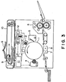
- Figure 3 illustrates an embodiment of the image forming apparatus according to the present invention.
- the image forming system may be operated as follows. First of all, an original G is set with its face to be reproduced directed downward onto an original table 10. Then, a copy button is pushed to start an copying operation. A unit 9 integrally incorporating an original illumination lamp, a short-focus lens array and a CCD sensor is moved to scanningly illuminate the original, whereby the illumination scanning beam carrying photosignals is focused by the short-focus lens array and enters the CCD sensor.
- the CCD sensor is composed of a light-receiving section, a transfer section and an output section.
- the photosignals are converted into electric signals (charge signals), which are transferred by the transfer section successively to the output section in synchronism with clock pulses.
- the charge signals are converted into voltage signals, which are amplified and converted into a low impedance form to be outputted.
- the thus formed analog signals are converted into digital signals, which are optimized by a controller 11 with respect to resolution and gradation depending on the image characteristics.of the original G and sent to a printer section including a charging means 3, a developing means 4 and a laser scanning unit 12, which are also controlled by the controller 11.
- image data is supplied directly from a computer which can be used in place of the controller 11, the image data is processed and converted by the computer to be supplied to the printer section while selecting mode of reproducing resolution and gradation so as to provide desirable images.
- image formation is performed in the following manner based on the above-supplied image signals.
- a photosensitive member 1 according to the present invention in the form of a drum is rotatively driven at a prescribed peripheral speed about a control shaft and, during the rotation thereof, is charged by a charging means 3, e.g., uniformly to a Prescribed voltage of a positive polarity or a negative polarity.
- the charged (applied) voltage on the photosensitive member 1 is controlled depending on image data such as the nature of the original image to be reproduced whether it is principally a binary image comprising characters, etc., or a gradational image, such as a photographic image, obtained by characterization of the original image during the above-mentioned conversion of the analog signals from the CCD light-receiving section into digital signals.
- the charging means 3 is controlled to provide a higher charged voltage so as to utilize a larger ⁇ and a larger induction energy.
- the charging means 3 is controlled to provide a lower charged voltage so as to utilize a smaller ⁇ and a smaller induction energy. For example, if the image to be outputted is all composed of binary images, a high voltage is applied depending on a required resolution thereof. If the image is principally composed of gradational images, a lower voltage is applied.
- the charging means 3 is controlled, for example, in this manner.
- the image to be outputted is composed of binary images and gradational images in mixture
- the voltage is controlled so as to optimize the induction energy and ⁇ of the photosensitive member depending on the characteristics of the mixture image.
- the applied voltage may be uniformly set for each original (sheet) based on the resolution and gradation thereof.
- it is also possible to set different applied voltages for regions having different image characteristics of an original e.g., in case where an original has substantially large regions clearly demarcated from each other because of image characteristics, such as a region composed primarily of binary images and a region primarily composed of gradational images.
- image characteristics such as a region composed primarily of binary images and a region primarily composed of gradational images.
- the charging means 3 may comprise a corona.charger, a roller charger, a brush charger, a magnetic brush charger or a blade charger. Further, in order to provide an imagewise varying voltage or regionally different applied voltages to considerably small regions, it is possible to use, e.g., an ionic flow charger as disclosed in U.S. Pat. No. 4,155,093.
- the thus-charged surface of the photosensitive member 1 is scanned with laser beam issued from a solid laser device turned ON and OFF depending on image signals and directed by a polygonal mirror rotating at a high speed in the laser scanning unit 12 to successively form latent images on the photosensitive member 1 corresponding to the original image.
- FIG 4 is an enlarged schematic illustration of a laser scanning unit 300 (corresponding to the unit 12 in Figure 3) for scanning a laser beam in the above-described image forming apparatus shown in Figure 3.
- a laser beam is emitted from a solid laser device 302 excited by emission signals supplied from an emission signal generator 301 based on image signals is converted by a collimator lens system 303, which are directed into an arrow C direction by a rotatory polygonal mirror 304 rotating in the direction of an arrow b and focused by f- ⁇ lenses 305a, 305b and 305c into a spot onto an illuminated surface 306 on the photosensitive drum (1 in Figure 3).
- the illuminated surface 306 is provided with an exposure energy distribution for one line of scanning image, and the illuminated surface 306 is scrolled by a prescribed width in a direction perpendicular to the scanning direction to form an exposure energy distribution on the illuminated surface 306 corresponding to given image signals.
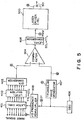
- a multi-value recording is also performed according to an areal gradation, mode based on a PWM (pulse width modulation) scheme, which will be described with reference to Figures 5 and 6, of which Figure 5 is a block diagram of an embodiment of a PWM circuit and Figure 6 is a time chart for illustrating the operation of the circuit.
- PWM pulse width modulation
- the PWM clrcuit includes a TTL latch circuit 401 for latching 8 bit-digital signals, a high speed level shifter for converting TTL logic levels into ECL logic levels, a high-speed D/A converter 403 for converting the ECL logic levels into analog signals.
- the PWM circuit further includes an ECL comparator for emitting PWM signals, a level converter 405 for converting ECL logic levels into TTL logic levels, a clock signal oscillator 406 for generating clock signals 2f, a triangular wave generator 407 for generating substantially ideal triangular wave signals synchronized with clock signals 2f, and a 1/2 frequency demultiplier 408 for subjecting the clock signals 2f to 1/2 frequency demultiplication to form image clock signals f. That is, the clock signals 2f have a frequency which is two times the frequency of the image clock signals f. For a high-speed operation of the circuit, some ECL logic circuits may be placed at desired parts.
- clock signals 2f and at (b) are shown clock signals f which are related with image signals as shown at (e). Also in the triangular wave generator 407, the clock signals 2f are 1/2 frequency-demultiplied to generate triangular signals (c), which are converted into triangular wave signals (d) by conversion into the ECL level.
- image signals (e) vary at 256 levels ranging from OOh (white) to FFh (black).
- some image signals are shown by ECL voltage levels after the D/A conversion. For example a black level of FFh is allotted to a first pixel; a halftone level of 80h, to a second pixel; a halftone level of 40h, to a third pixel; and a halftone level of 20h to a fourth pixel.
- the comparator 404 compares the triangular wave signals (d) and the image signals (e) to generate PWM signals having pulse widths T, t2, t3, t4, etc., corresponding to image densities to be formed.
- the PWM signals are then-converted into PWM signals (f) by conversion into a TTL level of 0 volt or 5 volts and then inputted to a laser drive circuit 500.
- the exposure period for each pixel is controlled to provide 256 gradation levels at the maximum for each pixel.
- the gradation control by the PWM scheme is adopted, but it is also possible to adopt an areal gradation scheme based on the dither method, a laser beam intensity modulation scheme or a combination of these schemes.
- An electrostatic latent image thus formed on the photosensitive member 1 is developed by a developing apparatus 4 in which a developing bias level applied to a developing sleeve may be controlled corresponding to the charged. voltage level on the photosensitive member, to form a toner image thereon, which is then electrostatically transferred by a transfer charger 7 to a transfer-receiving material.
- the transfer-receiving material carrying the toner image is electrostatically separated from the photosensitive member 1 by a separation charger 8 and conveyed to a fixing device, where the toner image is thermally fixed onto the transfer-receiving material to form a copy image thereon, followed by discharge.
- the surface of the photosensitive member 1 after the toner image transfer is subjected to removal of attached soiling materials, such as residual toner thereon by a cleaner 5, further electrically cleaned by a pre-exposure means 2 and re-used for repetitive image formation.
- image formation was performed by using an image forming apparatus substantially as described above, which included a semiconductor laser (12, 302) of 680 nm and 35 mW issuing a laser beam providing a spot diameter (1/e) of 60 ⁇ m on the photosensitive member 1.
- Gradation recording was performed based on the PWM scheme, and outputted images were used for measuring a minimum resolution spot diameter and evaluation of gradation density reproducibility with eyes.
- the photosensitive member When the photosensitive member was illuminated with a laser spot beam at an exposure energy of 0.8 ⁇ J/cm in the spot diameter (1/e) of 60 ⁇ m, and developed with a two component-type developer including a non-magnetic black toner having an average diameter of 8 ⁇ m under application of a bias voltage Vdc of 450 volts, the minimum resolution (Example 1) diameter was ca. 25 ⁇ m and the gradation reproducibility by the PWM scheme was good. The results are summarized in Table 1 appearing hereinafter.
- Example 1 The above-described procedure of Example 1 was repeated by charging the charged potential levels (Vd) on the photosensitive member to 300 volts, 200 volts, 700 volts and 100 volts, respectively, while satisfying a relationship of
- 50 volts and controlling the laser beam intensity be equal to the saturation sensitivities at the charged potential levels, similarly as in all Examples and Comparative Examples herein.
- 50 volts and controlling the laser beam intensity be equal to the saturation sensitivities at the charged potential levels, similarly as in all Examples and Comparative Examples herein.
- Table 1 The results are inclusively shown in Table 1.
- An aluminum cylinder of 80 mm in diameter and 360 mm in length as an electroconductive substrate was coated by dipping with a 5 % methanol solution of a polyamide ("AMILAN CM-8000" mfd. by Toray K.K.), followed by drying, to form a 1 ⁇ m-thick undercoating layer.
- AMILAN CM-8000 polyamide
- the charge generation layer was further coated with a solution of 90 wt. parts of 4-N,N-diethylaminobenzaldehydediphenylhydrazone an 100 wt. parts of polycarbonate resin ("NOVAREX", mfd. by Mitsubishi Kasei Kogyo K.K.) dissolved in chlorobenzene and dried at 120 °C for 1 hour to form a 22 ⁇ m-thick charge transport layer, thereby providing an electrophotographic photosensitive member of function-separation type.
- polycarbonate resin ("NOVAREX", mfd. by Mitsubishi Kasei Kogyo K.K.
- Photosensitive member was formed to provide a V - E curve at a charged voltage of -700 volts showing an induction energy of 0 and thus a ⁇ of 1.0.
- the photosensitive member was evaluated at a charged voltage of -700 volts with respect to image forming performances in the same manner as in Example 1, whereby a minimum resolution diameter was ca. 45 ⁇ m and the gradation reproducibility was inferior at highlight portions.
- the photosensitive member of Comparative Example 3 was evaluated at a charged voltage of -500 volts with respect to the V - E curve and the image forming performances. The results are shown in Table 1.
Landscapes
- Engineering & Computer Science (AREA)
- Microelectronics & Electronic Packaging (AREA)
- Physics & Mathematics (AREA)
- General Physics & Mathematics (AREA)
- Exposure Or Original Feeding In Electrophotography (AREA)
Applications Claiming Priority (3)
| Application Number | Priority Date | Filing Date | Title |
|---|---|---|---|
| JP14883794 | 1994-06-30 | ||
| JP14883794 | 1994-06-30 | ||
| JP148837/94 | 1994-06-30 |
Publications (2)
| Publication Number | Publication Date |
|---|---|
| EP0690357A1 true EP0690357A1 (de) | 1996-01-03 |
| EP0690357B1 EP0690357B1 (de) | 2000-02-09 |
Family
ID=15461847
Family Applications (1)
| Application Number | Title | Priority Date | Filing Date |
|---|---|---|---|
| EP95304593A Expired - Lifetime EP0690357B1 (de) | 1994-06-30 | 1995-06-29 | Elektrografisches Gerät und Bilderzeugungsverfahren |
Country Status (3)
| Country | Link |
|---|---|
| US (1) | US5666589A (de) |
| EP (1) | EP0690357B1 (de) |
| DE (1) | DE69514963T2 (de) |
Cited By (1)
| Publication number | Priority date | Publication date | Assignee | Title |
|---|---|---|---|---|
| EP0932085A4 (de) * | 1996-10-08 | 2002-04-10 | Ricoh Kk | Bilderzeugungsvorrichtung und bilderzeugungsverfahren |
Families Citing this family (15)
| Publication number | Priority date | Publication date | Assignee | Title |
|---|---|---|---|---|
| US6115576A (en) * | 1998-05-01 | 2000-09-05 | Ricoh Company, Ltd. | Image forming apparatus using a developing liquid and including an intermediate transfer body |
| KR20020020714A (ko) * | 2000-03-27 | 2002-03-15 | 마치오 나카지마 | 액정 셔터 |
| KR100396550B1 (ko) * | 2001-01-26 | 2003-09-03 | 삼성전자주식회사 | 전자사진 인쇄방법 |
| US7245851B2 (en) * | 2003-11-26 | 2007-07-17 | Canon Kabushiki Kaisha | Electrophotographic apparatus |
| CN101320235B (zh) * | 2008-05-21 | 2010-04-07 | 旭丽电子(广州)有限公司 | 彩色激光打印机及打印方法 |
| JP5081271B2 (ja) | 2009-04-23 | 2012-11-28 | キヤノン株式会社 | 電子写真感光体、プロセスカートリッジおよび電子写真装置 |
| JP4696174B2 (ja) | 2009-04-23 | 2011-06-08 | キヤノン株式会社 | 電子写真感光体の製造方法 |
| JP5610907B2 (ja) * | 2009-08-18 | 2014-10-22 | キヤノン株式会社 | 電子写真感光体、プロセスカートリッジおよび電子写真装置 |
| JP5734093B2 (ja) | 2010-06-30 | 2015-06-10 | キヤノン株式会社 | 電子写真感光体、プロセスカートリッジおよび電子写真装置 |
| JP5827612B2 (ja) | 2011-11-30 | 2015-12-02 | キヤノン株式会社 | ガリウムフタロシアニン結晶の製造方法、及び該ガリウムフタロシアニン結晶の製造方法を用いた電子写真感光体の製造方法 |
| JP5993720B2 (ja) | 2011-11-30 | 2016-09-14 | キヤノン株式会社 | 電子写真感光体、プロセスカートリッジおよび電子写真装置 |
| JP6071439B2 (ja) | 2011-11-30 | 2017-02-01 | キヤノン株式会社 | フタロシアニン結晶の製造方法、および電子写真感光体の製造方法 |
| JP6478750B2 (ja) | 2014-04-30 | 2019-03-06 | キヤノン株式会社 | 電子写真感光体、プロセスカートリッジおよび電子写真装置、ならびに、フタロシアニン結晶およびその製造方法 |
| JP2017083537A (ja) | 2015-10-23 | 2017-05-18 | キヤノン株式会社 | 電子写真感光体、プロセスカートリッジ及び電子写真装置 |
| US12235606B2 (en) | 2020-09-28 | 2025-02-25 | Canon Kabushiki Kaisha | Process cartridge |
Citations (6)
| Publication number | Priority date | Publication date | Assignee | Title |
|---|---|---|---|---|
| US4155093A (en) | 1977-08-12 | 1979-05-15 | Dennison Manufacturing Company | Method and apparatus for generating charged particles |
| JPH01169454A (ja) | 1987-12-25 | 1989-07-04 | Koichi Kinoshita | ディジタル光入力用感光体 |
| DE4126457A1 (de) * | 1990-08-10 | 1992-02-27 | Ricoh Kk | Bilderzeugungseinrichtung |
| US5241347A (en) * | 1990-11-29 | 1993-08-31 | Minolta Camera Kabushiki Kaisha | Image forming apparatus comprising means for automatically adjusting image density |
| EP0589131A2 (de) * | 1992-09-24 | 1994-03-30 | Kabushiki Kaisha Toshiba | Bilderzeugungsgerät und - verfahren |
| US5325122A (en) * | 1992-02-07 | 1994-06-28 | Minolta Camera Kabushiki Kaisha | Apparatus for forming digital images |
Family Cites Families (7)
| Publication number | Priority date | Publication date | Assignee | Title |
|---|---|---|---|---|
| JPH0664385B2 (ja) * | 1985-09-30 | 1994-08-22 | キヤノン株式会社 | 電子写真方法 |
| US4882257A (en) * | 1987-05-27 | 1989-11-21 | Canon Kabushiki Kaisha | Electrophotographic device |
| US5181071A (en) * | 1991-12-02 | 1993-01-19 | Yamanashi Electronics Co., Ltd. | Apparatus for evaluating characteristics of photosensitive drum for electrophotography |
| JP3143521B2 (ja) * | 1992-06-17 | 2001-03-07 | シャープ株式会社 | 電子画像形成装置 |
| JPH06230643A (ja) * | 1992-12-10 | 1994-08-19 | Minolta Camera Co Ltd | 画像濃度制御装置 |
| JP2773791B2 (ja) * | 1993-03-23 | 1998-07-09 | 三田工業株式会社 | 画像形成装置 |
| US5363174A (en) * | 1993-12-20 | 1994-11-08 | Xerox Corporation | Method and apparatus for background control in an electrostatographic printing machine |
-
1995
- 1995-06-29 EP EP95304593A patent/EP0690357B1/de not_active Expired - Lifetime
- 1995-06-29 DE DE69514963T patent/DE69514963T2/de not_active Expired - Lifetime
- 1995-06-30 US US08/497,420 patent/US5666589A/en not_active Expired - Lifetime
Patent Citations (6)
| Publication number | Priority date | Publication date | Assignee | Title |
|---|---|---|---|---|
| US4155093A (en) | 1977-08-12 | 1979-05-15 | Dennison Manufacturing Company | Method and apparatus for generating charged particles |
| JPH01169454A (ja) | 1987-12-25 | 1989-07-04 | Koichi Kinoshita | ディジタル光入力用感光体 |
| DE4126457A1 (de) * | 1990-08-10 | 1992-02-27 | Ricoh Kk | Bilderzeugungseinrichtung |
| US5241347A (en) * | 1990-11-29 | 1993-08-31 | Minolta Camera Kabushiki Kaisha | Image forming apparatus comprising means for automatically adjusting image density |
| US5325122A (en) * | 1992-02-07 | 1994-06-28 | Minolta Camera Kabushiki Kaisha | Apparatus for forming digital images |
| EP0589131A2 (de) * | 1992-09-24 | 1994-03-30 | Kabushiki Kaisha Toshiba | Bilderzeugungsgerät und - verfahren |
Cited By (2)
| Publication number | Priority date | Publication date | Assignee | Title |
|---|---|---|---|---|
| EP0932085A4 (de) * | 1996-10-08 | 2002-04-10 | Ricoh Kk | Bilderzeugungsvorrichtung und bilderzeugungsverfahren |
| EP1548514A1 (de) | 1996-10-08 | 2005-06-29 | Ricoh Co., Ltd. | Bilderzeugungsgerät und Verfahren zur Bilderzeugung |
Also Published As
| Publication number | Publication date |
|---|---|
| DE69514963T2 (de) | 2000-06-29 |
| EP0690357B1 (de) | 2000-02-09 |
| DE69514963D1 (de) | 2000-03-16 |
| US5666589A (en) | 1997-09-09 |
Similar Documents
| Publication | Publication Date | Title |
|---|---|---|
| EP0690357B1 (de) | Elektrografisches Gerät und Bilderzeugungsverfahren | |
| US6824939B2 (en) | Electrophotographic image forming method and apparatus | |
| US5818489A (en) | Image forming apparatus and process cartridge having exposure device using light beam having specific spot area | |
| JP2000206710A (ja) | 電子写真感光体及び電子写真画像形成法 | |
| US6205306B1 (en) | Electrophotographic apparatus | |
| JPH1130935A (ja) | 画像形成装置 | |
| JPH11202531A (ja) | 電子写真感光体及び電子写真画像形成装置 | |
| US6282393B1 (en) | Developing apparatus with alternating bias voltage | |
| JPH034232A (ja) | 電子写真感光体 | |
| JPH0876533A (ja) | 電子写真装置及び画像形成方法 | |
| JP4136622B2 (ja) | 画像形成装置及びプロセスカートリッジ | |
| JP2003270877A (ja) | 電子写真装置 | |
| JPH034231A (ja) | 電子写真感光体 | |
| JPH11202518A (ja) | 電子写真感光体 | |
| JPS63223751A (ja) | 電子写真感光体 | |
| JP3171300B2 (ja) | 電子写真感光体、電子写真装置及び電子写真装置ユニット | |
| JPH08185022A (ja) | 画像形成装置 | |
| JP3935392B2 (ja) | 電子写真感光体、該電子写真感光体を有する電子写真装置並びに電子写真ユニット | |
| JPH10282709A (ja) | 電子写真用被記録材およびそれを用いた画像形成装置 | |
| JPH1090933A (ja) | 電子写真用被記録材、及びそれを用いた画像形成装置 | |
| JPH10282695A (ja) | 電子写真感光体およびそれを用いた画像形成装置 | |
| JP2696399B2 (ja) | 画像形成方法及びその装置 | |
| JPH034230A (ja) | 電子写真感光体 | |
| JPH11198453A (ja) | 電子写真画像形成装置 | |
| JPH09211908A (ja) | 画像形成方法及びその装置 |
Legal Events
| Date | Code | Title | Description |
|---|---|---|---|
| PUAI | Public reference made under article 153(3) epc to a published international application that has entered the european phase |
Free format text: ORIGINAL CODE: 0009012 |
|
| AK | Designated contracting states |
Kind code of ref document: A1 Designated state(s): DE ES FR GB IT NL |
|
| 17P | Request for examination filed |
Effective date: 19960515 |
|
| 17Q | First examination report despatched |
Effective date: 19980225 |
|
| GRAG | Despatch of communication of intention to grant |
Free format text: ORIGINAL CODE: EPIDOS AGRA |
|
| GRAG | Despatch of communication of intention to grant |
Free format text: ORIGINAL CODE: EPIDOS AGRA |
|
| GRAG | Despatch of communication of intention to grant |
Free format text: ORIGINAL CODE: EPIDOS AGRA |
|
| GRAH | Despatch of communication of intention to grant a patent |
Free format text: ORIGINAL CODE: EPIDOS IGRA |
|
| GRAH | Despatch of communication of intention to grant a patent |
Free format text: ORIGINAL CODE: EPIDOS IGRA |
|
| GRAA | (expected) grant |
Free format text: ORIGINAL CODE: 0009210 |
|
| AK | Designated contracting states |
Kind code of ref document: B1 Designated state(s): DE ES FR GB IT NL |
|
| PG25 | Lapsed in a contracting state [announced via postgrant information from national office to epo] |
Ref country code: NL Free format text: LAPSE BECAUSE OF FAILURE TO SUBMIT A TRANSLATION OF THE DESCRIPTION OR TO PAY THE FEE WITHIN THE PRESCRIBED TIME-LIMIT Effective date: 20000209 Ref country code: IT Free format text: LAPSE BECAUSE OF FAILURE TO SUBMIT A TRANSLATION OF THE DESCRIPTION OR TO PAY THE FEE WITHIN THE PRESCRIBED TIME-LIMIT;WARNING: LAPSES OF ITALIAN PATENTS WITH EFFECTIVE DATE BEFORE 2007 MAY HAVE OCCURRED AT ANY TIME BEFORE 2007. THE CORRECT EFFECTIVE DATE MAY BE DIFFERENT FROM THE ONE RECORDED. Effective date: 20000209 Ref country code: ES Free format text: THE PATENT HAS BEEN ANNULLED BY A DECISION OF A NATIONAL AUTHORITY Effective date: 20000209 |
|
| REF | Corresponds to: |
Ref document number: 69514963 Country of ref document: DE Date of ref document: 20000316 |
|
| ET | Fr: translation filed | ||
| NLV1 | Nl: lapsed or annulled due to failure to fulfill the requirements of art. 29p and 29m of the patents act | ||
| PLBE | No opposition filed within time limit |
Free format text: ORIGINAL CODE: 0009261 |
|
| STAA | Information on the status of an ep patent application or granted ep patent |
Free format text: STATUS: NO OPPOSITION FILED WITHIN TIME LIMIT |
|
| 26N | No opposition filed | ||
| REG | Reference to a national code |
Ref country code: GB Ref legal event code: IF02 |
|
| REG | Reference to a national code |
Ref country code: FR Ref legal event code: ST Effective date: 20110228 |
|
| PG25 | Lapsed in a contracting state [announced via postgrant information from national office to epo] |
Ref country code: FR Free format text: LAPSE BECAUSE OF NON-PAYMENT OF DUE FEES Effective date: 20100630 |
|
| PGFP | Annual fee paid to national office [announced via postgrant information from national office to epo] |
Ref country code: GB Payment date: 20130624 Year of fee payment: 19 Ref country code: DE Payment date: 20130630 Year of fee payment: 19 |
|
| REG | Reference to a national code |
Ref country code: DE Ref legal event code: R119 Ref document number: 69514963 Country of ref document: DE |
|
| GBPC | Gb: european patent ceased through non-payment of renewal fee |
Effective date: 20140629 |
|
| REG | Reference to a national code |
Ref country code: DE Ref legal event code: R119 Ref document number: 69514963 Country of ref document: DE Effective date: 20150101 |
|
| PG25 | Lapsed in a contracting state [announced via postgrant information from national office to epo] |
Ref country code: DE Free format text: LAPSE BECAUSE OF NON-PAYMENT OF DUE FEES Effective date: 20150101 |
|
| PG25 | Lapsed in a contracting state [announced via postgrant information from national office to epo] |
Ref country code: GB Free format text: LAPSE BECAUSE OF NON-PAYMENT OF DUE FEES Effective date: 20140629 |
|
| PGFP | Annual fee paid to national office [announced via postgrant information from national office to epo] |
Ref country code: FR Payment date: 20090624 Year of fee payment: 15 |