EP0690499A2 - Empaquetage en plastique moulé pour puce semi-conductrice sans support - Google Patents
Empaquetage en plastique moulé pour puce semi-conductrice sans support Download PDFInfo
- Publication number
- EP0690499A2 EP0690499A2 EP95304597A EP95304597A EP0690499A2 EP 0690499 A2 EP0690499 A2 EP 0690499A2 EP 95304597 A EP95304597 A EP 95304597A EP 95304597 A EP95304597 A EP 95304597A EP 0690499 A2 EP0690499 A2 EP 0690499A2
- Authority
- EP
- European Patent Office
- Prior art keywords
- chip
- package
- semiconductor
- lead frame
- back surface
- Prior art date
- Legal status (The legal status is an assumption and is not a legal conclusion. Google has not performed a legal analysis and makes no representation as to the accuracy of the status listed.)
- Withdrawn
Links
Images


Classifications
-
- H—ELECTRICITY
- H10—SEMICONDUCTOR DEVICES; ELECTRIC SOLID-STATE DEVICES NOT OTHERWISE PROVIDED FOR
- H10W—GENERIC PACKAGES, INTERCONNECTIONS, CONNECTORS OR OTHER CONSTRUCTIONAL DETAILS OF DEVICES COVERED BY CLASS H10
- H10W74/00—Encapsulations, e.g. protective coatings
- H10W74/01—Manufacture or treatment
- H10W74/016—Manufacture or treatment using moulds
-
- H—ELECTRICITY
- H10—SEMICONDUCTOR DEVICES; ELECTRIC SOLID-STATE DEVICES NOT OTHERWISE PROVIDED FOR
- H10W—GENERIC PACKAGES, INTERCONNECTIONS, CONNECTORS OR OTHER CONSTRUCTIONAL DETAILS OF DEVICES COVERED BY CLASS H10
- H10W40/00—Arrangements for thermal protection or thermal control
- H10W40/70—Fillings or auxiliary members in containers or in encapsulations for thermal protection or control
- H10W40/77—Auxiliary members characterised by their shape
- H10W40/778—Auxiliary members characterised by their shape in encapsulations
-
- H—ELECTRICITY
- H10—SEMICONDUCTOR DEVICES; ELECTRIC SOLID-STATE DEVICES NOT OTHERWISE PROVIDED FOR
- H10W—GENERIC PACKAGES, INTERCONNECTIONS, CONNECTORS OR OTHER CONSTRUCTIONAL DETAILS OF DEVICES COVERED BY CLASS H10
- H10W70/00—Package substrates; Interposers; Redistribution layers [RDL]
- H10W70/40—Leadframes
- H10W70/475—Capacitors in combination with leadframes
-
- H—ELECTRICITY
- H10—SEMICONDUCTOR DEVICES; ELECTRIC SOLID-STATE DEVICES NOT OTHERWISE PROVIDED FOR
- H10W—GENERIC PACKAGES, INTERCONNECTIONS, CONNECTORS OR OTHER CONSTRUCTIONAL DETAILS OF DEVICES COVERED BY CLASS H10
- H10W74/00—Encapsulations, e.g. protective coatings
- H10W74/10—Encapsulations, e.g. protective coatings characterised by their shape or disposition
- H10W74/111—Encapsulations, e.g. protective coatings characterised by their shape or disposition the semiconductor body being completely enclosed
-
- H—ELECTRICITY
- H10—SEMICONDUCTOR DEVICES; ELECTRIC SOLID-STATE DEVICES NOT OTHERWISE PROVIDED FOR
- H10H—INORGANIC LIGHT-EMITTING SEMICONDUCTOR DEVICES HAVING POTENTIAL BARRIERS
- H10H20/00—Individual inorganic light-emitting semiconductor devices having potential barriers, e.g. light-emitting diodes [LED]
- H10H20/80—Constructional details
- H10H20/85—Packages
- H10H20/852—Encapsulations
- H10H20/853—Encapsulations characterised by their shape
-
- H—ELECTRICITY
- H10—SEMICONDUCTOR DEVICES; ELECTRIC SOLID-STATE DEVICES NOT OTHERWISE PROVIDED FOR
- H10H—INORGANIC LIGHT-EMITTING SEMICONDUCTOR DEVICES HAVING POTENTIAL BARRIERS
- H10H20/00—Individual inorganic light-emitting semiconductor devices having potential barriers, e.g. light-emitting diodes [LED]
- H10H20/80—Constructional details
- H10H20/85—Packages
- H10H20/858—Means for heat extraction or cooling
-
- H—ELECTRICITY
- H10—SEMICONDUCTOR DEVICES; ELECTRIC SOLID-STATE DEVICES NOT OTHERWISE PROVIDED FOR
- H10W—GENERIC PACKAGES, INTERCONNECTIONS, CONNECTORS OR OTHER CONSTRUCTIONAL DETAILS OF DEVICES COVERED BY CLASS H10
- H10W74/00—Encapsulations, e.g. protective coatings
-
- H—ELECTRICITY
- H10—SEMICONDUCTOR DEVICES; ELECTRIC SOLID-STATE DEVICES NOT OTHERWISE PROVIDED FOR
- H10W—GENERIC PACKAGES, INTERCONNECTIONS, CONNECTORS OR OTHER CONSTRUCTIONAL DETAILS OF DEVICES COVERED BY CLASS H10
- H10W74/00—Encapsulations, e.g. protective coatings
- H10W74/10—Encapsulations, e.g. protective coatings characterised by their shape or disposition
- H10W74/131—Encapsulations, e.g. protective coatings characterised by their shape or disposition the semiconductor body being only partially enclosed
- H10W74/142—Encapsulations, e.g. protective coatings characterised by their shape or disposition the semiconductor body being only partially enclosed the encapsulations exposing the passive side of the semiconductor body
-
- H—ELECTRICITY
- H10—SEMICONDUCTOR DEVICES; ELECTRIC SOLID-STATE DEVICES NOT OTHERWISE PROVIDED FOR
- H10W—GENERIC PACKAGES, INTERCONNECTIONS, CONNECTORS OR OTHER CONSTRUCTIONAL DETAILS OF DEVICES COVERED BY CLASS H10
- H10W90/00—Package configurations
- H10W90/701—Package configurations characterised by the relative positions of pads or connectors relative to package parts
- H10W90/751—Package configurations characterised by the relative positions of pads or connectors relative to package parts of bond wires
- H10W90/756—Package configurations characterised by the relative positions of pads or connectors relative to package parts of bond wires between a chip and a stacked lead frame, conducting package substrate or heat sink
Definitions
- the present invention relates to semiconductor devices, and, in particular, is directed to the packaging of a semiconductor chip.
- Packaging is one of the final steps in the process of manufacturing semiconductor chips.
- a fabricated semiconductor chip is mounted within a protective housing.
- the art of semiconductor chip technology has evolved far more rapidly than the integrally related technology of packaging the semiconductor chips.
- the packaging requirements of the newer, smaller, more powerful semiconductor chips are quickly progressing beyond the capabilities of traditional packaging technology and the conventional materials and designs presently utilized are fast becoming obsolete.
- the packaging demands of new semiconductors require configurations to accommodate increasing numbers of electrical interconnections, space constraints due to decreasing size, reduction in costs, improved reliability, and increasing heat transfer capabilities.
- the heat dissipating characteristics of semiconductor packages are measured by a network of heat transfer pathways through which heat must flow.
- the heat must be conducted from the chip through various thermal pathways to reach an outer surface of the package exposed to a cooling fluid, such as air.
- the fluid then convects away the heat.
- thermal conductivity The thermal conductivity of a material determines the amount of heat that can be conducted through that material. Some materials (such as metals) have high thermal conductivity, and other materials (such as rubber or glass) have low thermal conductivity.
- a package may have a multitude of various materials of various thermal conductivities through which heat must travel to reach the cooling fluid. This path may be tortuous when many materials with low thermal conductivities are encountered.
- heat transfer from the external surfaces of semiconductor packages is normally handled by the attachment of specially configured heat sinks which, generally, are mounted over the areas of greatest heat generation. This allows the heat to be conducted from the surface of the package, which usually has a low thermal conductivity, into the heat sink, which preferably has a high thermal conductivity and a large surface area. The heat then is convected away to the ambient air mass.
- the shapes of the heat sinks are configured to allow for a large surface area which increases heat convection away from the package. In previous applications, where the heat generation of semiconductor chips was moderate, the additional heat transfer capability created by externally bonding the heat sink to the package was sufficient to transfer any heat generated by the chip.
- a major heat transfer problem common to many semiconductor packages is the configuration of the package and the mounting location of the semiconductor chip.
- Advantageously locating the chip can eliminate several thermal boundaries and improve heat transfer. Because the chip is routinely attached to an internal substrate, the heat generated from the chip must pass through the attachment means to the substrate before it reaches the heat sink mounted on the outer surface of the package.
- the chip-substrate attachment bonding material adds thermal barriers to the package and limits the maximum heat transfer capability of the package.
- Plastic packages introduced decades ago, currently are utilized to package the vast majority of integrated circuits in the semiconductor chip industry. It is estimated that plastic packaging accounts for about 95 percent of the world market in semiconductor chip packaging (or about 40 billion parts per year).
- a typical plastic packaging operation involves the following sequence of steps:
- an improved plastic chip package has been developed, whereby the non-active back surface of a packaged semiconductor chip is exposed and facing outside of the package.
- This allows several advantages over conventional packaging: the chip to substrate epoxy attach process is eliminated; with no paddle or epoxy, the chip is situated at one face of the package, allowing ample room for bond wire loops, while still making the package thinner; the chip is exposed for direct attachment of a heat sink; less materials means less mismatched material properties, materials with thermal coefficients of expansion (TCE's) and strength different from silicon are eliminated, thereby improving internal stresses and attendant reliability; and cost savings are realized because less materials means less potential manufacturing problems and fewer assembly steps.
- TCE's thermal coefficients of expansion
- the invention in its broad form resides in a molded plastic semiconductor chip package as recited in Claim 1, and a method of forming a molded plastic semiconductor chip package as recited in Claim 13.
- a molded plastic semiconductor chip package comprises a conventional leadframe member, featuring, however, an opening therein, where typically a paddle mounting platform would have been provided.
- a semiconductor chip having an active front side surface and a nonactive back surface, is positioned within said opening, with the nonactive back surface of the chip fully unsupported by said lead frame. Bonding wires extend between the active front side of the chip and bonding pads of the lead frame.
- a molded plastic body encases the lead frame, bonding wires, and the semiconductor chip, with the nonactive back surface of the chip exposed and facing outside the package. If a heat sink is required, it can be attached in direct contact to the exposed back surface of the chip, for efficient and effective heat dissipation.
- the present improved package can be made by a process which features simplified steps in comparison with conventional molded plastic package assembly.
- a semiconductor chip is positioned within an opening of a lead frame.
- the opening of the lead frame has lateral dimensions greater than those of the chip.
- the chip initially is held in place in a fixture, preferably by vacuum.
- the leadframe is held in the same fixture either by vacuum means or other conventional means. While held in the fixture, the chip is wire bonded to the lead frame. Conventional ball or stitch bonding may be used.
- the chip and lead frame form a partially completed assembly with structural integrity sufficient to withstand normal handling.
- the assembly may be removed from the wire bonding fixture at this point, with the chip held in free space supported only by the bond wires.
- the chip and lead frame assembly is placed into a plastic package mold and held in place as plastic is transferred into the mold, thereby encasing the chip, bond wires, and leads.
- the back surface of the chip be positioned on a pedestal in the mold.
- the pedestal is equipped with a vacuum port to assist in maintaining the chip in position.
- plastic encases the chip, except the area of the chip back surface which was in contact with, and accordingly shielded by, the support pedestal. This thus leaves the nonactive back surface of the chip exposed and facing outside the package. If a heat sink is required, it readily can be attached directly to the exposed back surface of the chip.
- Figures 1-3 are cross-sectional views depicting sequential steps in the process for making the molded plastic semiconductor chip package of a preferred embodiment the present invention.
- Figure 4 is a cross sectional view of one embodiment of a semiconductor package according to a preferred embodiment the invention.
- Figure 5 is a cross sectional view of a fully assembled semiconductor package according to a preferred embodiment the present invention, including an attached heat sink element.
- Figures 6-13 are sectional views of additional embodiments of semiconductor packages according to a preferred embodiment the present invention.
- a semiconductor chip 20 is shown positioned on a fixture pedestal 21, which is equipped with a vacuum port 22 to assist in holding the chip securely in place during the wire bonding operation. While the chip 20 and lead frame 23 are held on the fixture, bondwires 24 are attached between the active side (26) of the chip 20 and the lead frame by an appropriate ball or stitch bonder (not shown). Once the . bondwires are in place, the partially completed assembly 25 (shown in Figure 2) may be removed from the wire bonding fixture. The chip 20, supported only by bondwires 24 has sufficient integrity to allow removal from the bonding fixture and handling of the partially completed assembly, to accommodate transport to the next subsequent process stage. Alternatively, the chip-lead frame assembly may remain in the fixture to travel to the next stage.
- the chip 20, wirebonded to lead frame 23, is placed in a mold bottom 38 and the non-active back surface 27 of chip 20 is positioned over mold fixture pedestal 28.
- the pedestal features vacuum port 29 to assist in holding the chip in place during the molding process.
- the plastic package comprises the chip 20, attached by bondwires 24 and lead frame 23, all. encased within plastic molded body 32.
- the portion of the chip back surface 27 previously positioned on the vacuum mold pedestal remains uncovered by plastic and is exposed and facing outside the package within recess 33.
- a finished molded plastic package including a heat sink 34 fitted into recess 33 in direct thermal contact with the exposed, nonactive back surface 27 of semiconductor chip 20.
- Figure 6 shows an embodiment of the invention designed to create a package featuring the back surface 27 of an encased semiconductor chip 20 which is flush with exterior surface 35 of the molded plastic body 32 rather than recessed within.
- This embodiment offers the advantages of a very thin, lightweight package which can accept a variety of heat sink designs.
- the leads may exit the mid plane of the plastic, or may be adjusted to accommodate manufacturing steps or applications.
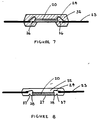
- the embodiment of Figure 7 includes a stress reducing ring 36 molded into the plastic material of molded body 32 to reduce stresses and consequent delaminations between the plastic and the chip 20.
- the ring could be made of any suitable material chosen for its specific mechanical or electrical properties.
- the ring may consist of lead frame material.
- the ring is situated such that it surrounds the outside edges of the chip 20 but is not in contact with it.
- the ring may be held in place, during the molding operation, by another vacuum port, in which case, a portion of the ring would be exposed.
- the ring may also be an integral part of the leadframe, i.e., it would be held in place by an adhesive between the leadframe and the ring.
- FIG. 8 A second embodiment with a different stress-reducing feature is illustrated in Figure 8.
- the plastic At the silicon/plastic/air interface 38, there is a tendency for the plastic to pull away from the silicon, since the plastic in that area is shrinking while it is cooling from the transfer molding temperature, and it shrinks more than the silicon. This difference in thermal contraction creates tension at the silicon/plastic/air interface, often leading to separation. In order to maintain tight contact to seal the joint from the atmosphere, the tension needs to be reduced. Accordingly, a notch 37 is built into the plastic mold body 32 to isolate most of the influence of the plastic body from the joint area. Such a notch readily could be formed, for example, by a positive feature in the mold bottom, and could take on one of various shapes and configurations.
- a relief notch 41 is provided in the top side of the molded plastic body. Such a relief notch serves to reduce package bending caused by the different coefficients of thermal expansion and chip stress.
- Figure 10 depicts a similar chip package, but featuring a stress relieving insert 43 built into the top side of the molded plastic body.
- This insert may be made of any suitable material or combination of materials, such as low-expansion silicon, metal, ceramic, and the like. The insert may be positioned by holding it in place during molding with a vacuum port in the top half of the mold. Alternatively, as shown in Figure 11, the insert may be held in place by bumps 45 which may be made of an elastic or plastic material, or other materials. As well as providing stress relief, the insert additionally may serve other functions.
- insert 47 may be a chip capacitor with bumps 45 forming electrical connections to chip 20, in order to provide power supply stabilization. It may also enhance the thermal cooling of the chip.
- the insert 43 may take on various thicknesses, lengths or widths, and it may be configured to have perforations or other shapes.
- Figure 12 demonstrates another approach to enhance control of deformations caused by thermal coefficient of expansion (TCE), and reduce cracking and moisture ingress.
- This embodiment includes a cover or foil 49 on the top side of the package, and cover or foil 51 on the bottom side. It could be held in place during molding or added later.
- the embodiment illustrated in Figure 13 features a package with both active front side 53 and non-active back surface 27 exposure of chip 20. Such an arrangement might better accommodate electrical connections, testing, enhanced cooling, stress reduction, optical interconnect, and/or an addition wire bonding sequence, and the like.
Landscapes
- Cooling Or The Like Of Semiconductors Or Solid State Devices (AREA)
Applications Claiming Priority (2)
| Application Number | Priority Date | Filing Date | Title |
|---|---|---|---|
| US26926494A | 1994-06-30 | 1994-06-30 | |
| US269264 | 1994-06-30 |
Publications (2)
| Publication Number | Publication Date |
|---|---|
| EP0690499A2 true EP0690499A2 (fr) | 1996-01-03 |
| EP0690499A3 EP0690499A3 (fr) | 1997-05-28 |
Family
ID=23026523
Family Applications (1)
| Application Number | Title | Priority Date | Filing Date |
|---|---|---|---|
| EP95304597A Withdrawn EP0690499A3 (fr) | 1994-06-30 | 1995-06-29 | Empaquetage en plastique moulé pour puce semi-conductrice sans support |
Country Status (1)
| Country | Link |
|---|---|
| EP (1) | EP0690499A3 (fr) |
Cited By (7)
| Publication number | Priority date | Publication date | Assignee | Title |
|---|---|---|---|---|
| EP0776039A3 (fr) * | 1995-11-21 | 1999-04-07 | Texas Instruments Incorporated | Améliorations pour des boítiers à semi-conducteurs |
| US5981312A (en) * | 1997-06-27 | 1999-11-09 | International Business Machines Corporation | Method for injection molded flip chip encapsulation |
| US5997798A (en) * | 1997-06-27 | 1999-12-07 | International Business Machines Corporation | Biasing mold for integrated circuit chip assembly encapsulation |
| US6552263B2 (en) | 1997-06-27 | 2003-04-22 | International Business Machines Corporation | Method of injection molded flip chip encapsulation |
| DE102004021838A1 (de) * | 2004-05-04 | 2005-09-08 | Infineon Technologies Ag | Halbleiterbauelement mit Kühlvorrichtung |
| US7529093B2 (en) | 2004-11-26 | 2009-05-05 | Sanyo Electric Co., Ltd. | Circuit device |
| WO2024178963A1 (fr) * | 2023-02-28 | 2024-09-06 | 华为数字能源技术有限公司 | Dispositif d'alimentation et module d'alimentation |
Family Cites Families (4)
| Publication number | Priority date | Publication date | Assignee | Title |
|---|---|---|---|---|
| JPH01136356A (ja) * | 1987-11-24 | 1989-05-29 | Nec Corp | 樹脂封止型半導体装置 |
| JPH01241831A (ja) * | 1988-03-23 | 1989-09-26 | Nec Corp | 半導体集積回路装置の樹脂封止方法 |
| JPH0223640A (ja) * | 1988-07-13 | 1990-01-25 | Hitachi Ltd | 樹脂封止型半導体装置 |
| JPH02277259A (ja) * | 1989-04-19 | 1990-11-13 | Mitsubishi Electric Corp | 半導体装置 |
-
1995
- 1995-06-29 EP EP95304597A patent/EP0690499A3/fr not_active Withdrawn
Non-Patent Citations (1)
| Title |
|---|
| None |
Cited By (10)
| Publication number | Priority date | Publication date | Assignee | Title |
|---|---|---|---|---|
| EP0776039A3 (fr) * | 1995-11-21 | 1999-04-07 | Texas Instruments Incorporated | Améliorations pour des boítiers à semi-conducteurs |
| US5981312A (en) * | 1997-06-27 | 1999-11-09 | International Business Machines Corporation | Method for injection molded flip chip encapsulation |
| US5997798A (en) * | 1997-06-27 | 1999-12-07 | International Business Machines Corporation | Biasing mold for integrated circuit chip assembly encapsulation |
| US6369449B2 (en) | 1997-06-27 | 2002-04-09 | International Business Machines Corporation | Method and apparatus for injection molded flip chip encapsulation |
| US6552263B2 (en) | 1997-06-27 | 2003-04-22 | International Business Machines Corporation | Method of injection molded flip chip encapsulation |
| US6570261B2 (en) | 1997-06-27 | 2003-05-27 | International Business Machines Corporation | Method and apparatus for injection molded flip chip encapsulation |
| DE102004021838A1 (de) * | 2004-05-04 | 2005-09-08 | Infineon Technologies Ag | Halbleiterbauelement mit Kühlvorrichtung |
| US7529093B2 (en) | 2004-11-26 | 2009-05-05 | Sanyo Electric Co., Ltd. | Circuit device |
| CN1783487B (zh) * | 2004-11-26 | 2012-06-13 | 三洋电机株式会社 | 电路装置及其制造方法 |
| WO2024178963A1 (fr) * | 2023-02-28 | 2024-09-06 | 华为数字能源技术有限公司 | Dispositif d'alimentation et module d'alimentation |
Also Published As
| Publication number | Publication date |
|---|---|
| EP0690499A3 (fr) | 1997-05-28 |
Similar Documents
| Publication | Publication Date | Title |
|---|---|---|
| US5604376A (en) | Paddleless molded plastic semiconductor chip package | |
| US5687474A (en) | Method of assembling and cooling a package structure with accessible chip | |
| US5869883A (en) | Packaging of semiconductor circuit in pre-molded plastic package | |
| US7061080B2 (en) | Power module package having improved heat dissipating capability | |
| US5483098A (en) | Drop-in heat sink package with window frame flag | |
| US5177669A (en) | Molded ring integrated circuit package | |
| KR100194848B1 (ko) | 성형 반도체 팩케지 | |
| US6271581B2 (en) | Semiconductor package structure having universal lead frame and heat sink | |
| JP4571320B2 (ja) | 半導体チップパッケージ | |
| US5822848A (en) | Lead frame having a detachable and interchangeable die-attach paddle | |
| CN1031446A (zh) | 用带式自动焊接法焊接的半导体芯片管壳 | |
| JPH08293524A (ja) | 半導体装置およびその製造方法 | |
| US20020135076A1 (en) | Heat sink with collapse structure and semiconductor package with heat sink | |
| US5652184A (en) | Method of manufacturing a thin semiconductor package having many pins and likely to dissipate heat | |
| US6507122B2 (en) | Pre-bond encapsulation of area array terminated chip and wafer scale packages | |
| KR20080015724A (ko) | 몰딩된 리드 부착물을 갖는 플라스틱 오버몰딩된 패키지들 | |
| US6075282A (en) | Leadframe for a semiconductor device and associated method | |
| US20050275089A1 (en) | Package and method for packaging an integrated circuit die | |
| EP0690499A2 (fr) | Empaquetage en plastique moulé pour puce semi-conductrice sans support | |
| US20060170080A1 (en) | Semiconductor device having directly attached heat spreader | |
| JPH02306654A (ja) | 半導体装置およびこれを用いた電子装置 | |
| JPH10112519A (ja) | 熱放散手段を有する集積回路装置及びその製造方法 | |
| US6979900B2 (en) | Integrated circuit package with integral leadframe convector and method therefor | |
| JPH05275578A (ja) | 半導体装置 | |
| JPS61125142A (ja) | 電子装置 |
Legal Events
| Date | Code | Title | Description |
|---|---|---|---|
| PUAI | Public reference made under article 153(3) epc to a published international application that has entered the european phase |
Free format text: ORIGINAL CODE: 0009012 |
|
| AK | Designated contracting states |
Kind code of ref document: A2 Designated state(s): DE FR GB IT NL |
|
| PUAL | Search report despatched |
Free format text: ORIGINAL CODE: 0009013 |
|
| AK | Designated contracting states |
Kind code of ref document: A3 Designated state(s): DE FR GB IT NL |
|
| 17P | Request for examination filed |
Effective date: 19970613 |
|
| 17Q | First examination report despatched |
Effective date: 19990310 |
|
| STAA | Information on the status of an ep patent application or granted ep patent |
Free format text: STATUS: THE APPLICATION IS DEEMED TO BE WITHDRAWN |
|
| 18D | Application deemed to be withdrawn |
Effective date: 19990721 |